國 立 交 通 大 學
應用化學研究所
博 士 論 文
自身模板輔助成長碳化矽奈米結構
Self-Templating Assisted Growth of Silicon Carbide
Nanostructures
研 究 生:王嘉興
指導教授:裘性天 博士
自身模板輔助成長碳化矽奈米結構
Self-Templating Assisted Growth of Silicon Carbide
Nanostructures
研 究 生: 王嘉興 Student:Chia-Hsin Wang
指導教授: 裘性天 博士 Advisor:Dr. Hsin-Tien Chiu
國 立 交 通 大 學
應 用 化 學 研 究 所
博 士 論 文
A Thesis
Submitted to Institute of Applied chemistry College of Science
National Chiao Tung University in Partial Fulfillment of the Requirements
for the Degree of Doctor of Science in
Applied chemistry July 2007
Hsinchu, Taiwan, Republic of China
Contents
Page
English Abstract i
Chinease Abstract iii
Acknowledgments v
Contents of Schemes and Tables vii
List of Figures viii
Chapter 1 Introduction 1
1.1 Introduction 1
1.2 Structure and Properties of SiC 2
1.2.1 Structure of SiC 2
1.2.2 Properties of SiC 3
1.3 Synthetic Methods of SiC 5
1.4 Nanostructures of SiC 8
1.4.1 SiC Nanocrystals 8
1.4.2 One-Dimensional SiC Nanostructures 9
1.4.2-1.1 SiC Nanorod and Nanowires from Hard Template Methods 10 1.4.2-1.2 SiC Nanorod and Nanowires from Vapor-Liquid-Solid Methods 10 1.4.2-1.3 SiC Nanorod and Nanowires from Vapor-Solid Methods 11
1.4.2-2 Tubular SiC 12
1.4.3 Porous SiC Nanostructure 12
1.5 Goal of This Thesis 13
1.6 References 14
Chapter 2 Silicon Carbide Nanostructures from Reactions between Vapors of Organochlorosilanes and Liquid of Sodium - Factors Affecting
Morphology and Composition 21
2.1 Introduction 21
2.2 Experimental 22
2.2.1 Materials 22
2.2.2 Synthesis of Sample DD from Me2SiCl2 and Na 22
2.2.3 Characterization 22
2.3 Results 23
2.3.2 SEM Characterizations 28 2.3.3 XRD Studies 31 2.3.4 TEM Characterizations 32 2.4 Discussion 35 2.5 Conclusions 38 2.6 References 40
Chapter 3 Growth of Polycrystalline Tubular Silicon Carbide - Yajima-Type
Reaction at the Vapor-Solid Interface 42
3.1 Introduction 42
3.2 Experimental Section 42
3.3 Results and Discussion 44
3.3.1 SEM and XRD Characterizations 46
3.3.2 TEM Studies 47
3.3.3 TGA Studies 53
3.3.4 Proposed Reaction Pathway 55
3.4 Field Emission Property Studies 56
3.5 Conclusions 57
3.6 References 59
3.7 Appendix 62
Chapter 4 Synthesis of Pseudo Thin Plate Silicon Carbide Nanostructure- Another
Case of Yajima-Type Reaction at the Vapor-Solid Interface 66
4.1 Introduction 66
4.2 Experimental Section 66
4.3 Results and Disscussion 67
4.3.1 Characterizations of the Yellow Product Prepared from Mg and MeSiHCl2 67
4.3.2 Characterizations of the Yellow Product Prepared from Mg and Me2SiCl2 70
4.3.3 Proposed Reaction Pathway 72
4.4 Comparison with Previous Reports through VSRG Process 72
4.5 Conclusions 74
4.6 References 75
Chapter 5 Deposition of Mesoporous Silicon Carbide Thin Films from
5.1 Introduction 76
5.2 Experimental Section 77
5.2.1 Materials. 77
5.2.2 Growth of Sn/amorphous SixC1-x Thin Films, I 77
5.2.3 Preparation of Samples I-P, I-P-HF, II, III, and IV 78
5.2.4 Preparation of n-type β-SiC/p-type Si Heterojunction 78
5.2.5 Characterization 78
5.3 Results and Discussion 79
5.3.1 Growth and Characterization of Sn/amorphous SixC1-x Thin Films 79
5.3.2 Mesoporous Amorphous SixC1-x (x = 0.3) Thin Films 86
5.3.3 Mesoporous β-SiC Thin Films 89
5.3.4 Electrical Property Studies 91
5.3.5 Reaction Pathway Elucidation 94
5.4 Conclusions 96
5.5 References 97
Chapter 6 Synthesis of Gold Nanowires via Galvanic Displacement Reaction 102
6.1 Introduction 102
6.2 Experimental 102
6.2.1 Synthesis of Gold Nanowires 102
6.2.2 Characterization 103
6.3 Result and Discussion 103
6.3.1 Characterizations of Gold Nanowires 103
6.3.2 Proposed Growth Mechanism of Au Nanowires 105
6.4 Conclusions 106
6.5 References 107
Self-Templating Assisted Growth of Silicon Carbide Nanostructures
Student: Chia-Hsin Wang Advisor: Dr. Hsin-Tien Chiu
Institute of Applied Chemistry, National Chiao Tung University
Abstract:
In this thesis, we employ phase segregation as the concept to develop diverse SiC nanostructures via vapor-liquid and vapor-solid reactions. Inorganic salts MClx (M=Na,
Mg, Ca) act as templates generated in-situ to assist the morphology development.
First, cubic shells and spherical nanoparticles of β-SiC were produced at 1273 K by processing the ceramic precursors formed from the reactions between vapor of organochlorosilanes, Me2SiCl2, MeSiCl3, MeSiHCl2, and PhSiCl3, and liquid Na at 523 –
723 K. From Me2SiCl2, a flexible linear polycarbosilane precursor was synthesized and
covered the NaCl byproduct surface to from a cubic shape. Hollow cubic β-SiC shells were produced after the NaCl templates were removed. From MeSiCl3, a rigid
cross-linked polycarbosilane was produced and phase segregated from the NaCl byproduct. The precursor was transformed into nanoparticles without special morphology. MeSiHCl2 produced a cross-linked polysilane precursor at low
temperatures, which can be converted into a mixture of β-SiC and Si nanoparticles. At high temperatures, the polysilane converted to polycarbosilane and produced hollow cubic β-SiC shells. The carbon-rich PhSiCl3 generated cube-like particles as the final
product, which contained β-SiC and carbon.
In the second section, polycrystalline tubular SiC on Si was prepared by reacting MeSiHCl2 vapor and Ca thin film on Si at 773 - 923 K followed by heat-treatment at
of a core of CaCl2 and a shell of SiCxHy. After removal of the CaCl2 core, the layer of
polycrystalline SiC tubes on Si emitted electrons at a low applied field of 2.5 V/μm with a current of 10 μA/cm2.
In the third section, we also used the phase segregation concept in the reaction of Me2SiCl2 and MeHSiCl2 between and magnesium metal at 823 - 923 K. The product was
heat treated at 1273 K under vacuum. It showed pseudo thin plate SiC nanostructure, which was self-templated by MgCl2 generated in situ.
In the fourth section, we extended the phase segregation idea to create porous SiC thin film on Si subtrate. Using Sn(SiMe3)4 as the precursor,amorphous SixC1-xthin films
with Sn nanoparticles embedded were grown on Si substrates at 923 K by low pressure chemical vapor deposition. After treated under hydrogen plasma at 923 K, the Sn nanoparticles in the films were removed by an HF solution and by evaporation at 1423 K. Following the removal of Sn, high temperature treatments at 1273 - 1423 K converted the amorphous thin films into mesoporous semiconducting β-SiC thin films with pore sizes10 - 100nm.
Finally, one dimensional high aspect ratio Au nanowires were fabricated via galvanic reduction of HAuCl4 solution in the presence of cetyltrimethylammonium
chloride (CTAC) by the Sn nanoparticles embedded in amorphous the SixC1-x thin film
自身模板輔助成長碳化矽奈米結構
研究生:王嘉興 指導教授:裘性天 博士 國立交通大學應用化學所摘 要
在本論文裡,我們利用相分離的概念,藉由在氣液或氣固界面的化學反應來成長碳 化矽奈米結構。反應過程中,自我生成的無機鹽類氯化鈉,氯化鎂,以及氯化鈣提供了 形成奈米碳化矽形貌的模板。 首先,利用不同的氣態有機碳氯矽烷,二氯二甲基矽烷、三氯甲基矽烷、二氯甲基 矽烷,和三氯苯基矽烷在523 -723 K 下與液態的金屬鈉反應生成碳化矽的前驅物以及副 產物氯化鈉。然後經過1273 K 的熱處理,生成方形籠狀或圓球型態的碳化矽奈米結構。 在利用氣態二氯二甲基矽烷反應時,一開始會生成具可撓曲的線性聚碳矽烷化合物覆著 在副產物氯化鈉的表面上。經過熱處理後,可以移除氯化鈉,進而生成方形空心的碳化 矽。使用三氯甲基矽烷反應時,則會生成硬性網狀聚碳矽烷化合物與副產物氯化鈉產生 相分離,最後移去氯化鈉時,則得到圓球形狀的碳化矽奈米顆粒。然而在使用二氯甲基 矽烷時,會因為反應溫度不同而生成不同型態的聚碳矽化合物。在較低溫下會產生硬性 聚碳矽烷化合物,進而生成圓球形狀的碳化矽與矽奈米顆粒;而在較高溫度則是生成可 撓曲的線性聚碳矽烷化合物,進而生成方形空心的碳化矽。除此之外,如果是具有較多 碳的三氯苯基矽烷當前驅物,則會生成類方形碳/碳化矽空心顆粒。 在第二部份,我們利用物理氣相沈積的方法先在矽基材上沈積一層鈣薄膜。然後利 用二氯甲基矽烷與鈣金屬在773 – 923 K 反應 14 小時,之後經過 1273 K 的熱處理,就 可以成功的合成出空心長條型態的碳化矽奈米結構。主要的原因是反應一開始副產物氯 化鈣會與聚碳矽化合物相分離形成核殼狀的一維型態的產物,而經高溫處理氯化鈣被移 除,聚碳矽化合物進而形成空心長條型態碳化矽結構。空心長條型態碳化矽結構可以用於場發射的應用,實驗發現只需要提供相當低的電場2.5 V/ μm 就會有 10 μA/cm2 電流 密度的產生。 第三部分,我們再次驗證相分離的概念。藉由二氯甲基矽烷或二氯二甲基矽烷與氫 氣電漿處理過後的鎂金屬在823 K 或 923 K 下反應,之後在 1273 K 高溫熱處理,即可 得到藉由自我產生的片狀氯化鎂模板的輔助,得到片狀碳化矽結構。 而在第四部份,我們將相分離的概念延伸到在矽基材上製作孔洞性的碳化矽薄膜。 利用Sn(SiMe3)4 當作化學氣相沈積的前驅物,一開始先在 923 K 下成長薄膜;此時奈米 錫顆粒會與無晶相的矽碳化合物產生相分離,而形成錫奈米顆粒鑲埋在矽碳化合物的薄 膜。之後利用HF 水溶液或在 1423 K 的高溫真空下將利用氫氣電漿在薄膜上的錫顆粒移 除,即可生成孔洞碳化矽薄膜。我們也利用離子佈值的方式,將磷摻雜到P-type 矽基材 上的孔洞碳化矽薄膜,使其展現更好的heterojunction diode 的性質。 最後,我們也利用錫奈米顆粒鑲埋在矽碳化合物的薄膜當作還原劑。藉由錫顆粒與 金氯酸在具有氯化十六烷基三甲基銨鹽(CTAC)的水溶液下,行自發性的賈凡尼置換反 應,在矽碳化合物的薄膜表面上生成一維的金奈米線。
Acknowledgments
五年了,想不到我來交大已經有五年的時間了好像又念了一次大學一樣,新竹像埔 里一樣我又多了另一個第二個家。雖然時間差不多,但是所經歷的以及所學到的是截然 不同的。五年的研究生生活裡酸甜苦辣的日子都有,曾經為了趕 data 整夜不睡,曾經 為了實驗結果不好而整夜難眠,但這些研究上的煩惱都會因實驗室歡樂的環境、實驗室 夥伴門的相互討論、鼓勵及老師們的細心指導都會一一的迎刃而解。經過這五年的歷 練,除了在學業知識方面學習到許多不同的東西外,在於生活與人生觀上也得到很多的 啟發。這一切的提升,要感謝許多人支持與鼓勵。 首先,感謝指導教授裘性天教授在這段期間提供我一個相當優良的學習環境,讓我 能夠充分學習、自由發揮,同時也要感謝老師在於研究思考方面的指導與開示,使我的 思想更加廣闊、更加深遠。另外要特別感謝老師這一年來辛苦的幫我修改論文,讓我能 夠順利的完成此篇論文。還有感謝一起 meeting 的李紫原教授在於實驗上的建議與指 導,使得我的實驗能夠順利進行且更加的完備。 其次,感謝口試委員陳登銘教授與李積琛教授,不只在口試的時間指導我,且平時 也會提供一些建議及實驗上的協助。此外也要感謝口試委員吳季珍教授,百忙當中從台 南遠道而來指導我,使的我的論文能夠更加的完善。 還有感謝清交兩邊實驗室裡的大大小小,讓我在一個快樂的環境裡生活與學習。首 先,感謝在交大實驗室的夥伴們,大學長張裕煦博士現在的張教授在我一開始進入實驗 室時的教導,讓我受益良多。此外簡俊雄學長、閻明宇學長、周宜萱學姊、彭志偉學長、 王隆昇學長、盛焙蓀學姊、陳盈薰學姊、夏志豪學長,還有同學及學弟妹,子厚、文昭、 志豪、曜安、亭凱、進興、高翔、惶凱、蕭蕭、宇婕、sif、嘉芳、goby、昕君、季勳、 大隻、馨緯、文志、大銘、妍如,大家在實驗室上的相互幫忙及一起玩樂,讓我的研究 生活多彩繽紛。 另外也要感謝在清大實驗室的伙伴們,正得學長、鈺芬學姐,學弟們、旻橋、奕仁、 聰盈、諺百、鑑嘉,雖然相處時間不多,但也不時的提供了許多實驗上的幫助,讓我實驗更加的豐富。
還要感謝大學的同學俊邦、澄明、仲德、幫主在週末時、特殊節慶裡能夠一起吃飯 聊天或則一起出遊,使我備感溫馨沒有孤單寂寞的感覺。
最後感謝我的家人,給於我無限的自由且能夠容忍念這麼久的時間,讓我順利的完 成學業。還有相當感謝上天讓我幸運的遇到這麼多關心我、照顧我的貴人。謝謝。
Contents of Schemes and Tables
Page
Chapter 1
Table 1.1 Physical properties of the most common SiC polytypes. 4
Table 1.2 Electric properties of SiC and other semiconductors. 5
Chapter 2
Scheme 2.1 Summary of reaction processes. 23
Table 2.1 Summary of reactions between sodium and organochlorosilanes. 24
Table 2.2 FT-IR absorptions of the ceramic precursors. 27
Scheme 2.2 Proposed conversions of methylchlorosilanes to ceramic precursors. 36
Chapter 3
Scheme 3.1 Reaction steps to form tubular SiC on Si wafer. 55
Chapter 4
Scheme 4.1 Reaction steps to form pseudo thin plate SiC nanostructure. 72
Chapter 5
Table 5.1 Summary of samples. 82
Scheme 5.1 Reaction steps to form II, mesoporous amorphous SixC1-x (x = 0.3)
and III, β-SiC thin films 96
Chapter 6
List of Figures
Page Chapetr 1
Figure 1.1 The unit cell of 3C-SiC. The distance, a, between neighboring silicon,
and C-Si are approximately 0.308 nm, and 0.189 nm, respectively.
2
Figure 1.2 The stacking sequence of double layers of the most common SiC
polytypes.
3
Chapter 2
Figure 2.1 SEM images of (A) Pre-DD, and (B) Pre-MT. (C) XRD pattern of Pre-DD. (Au was sputtered to increase conductivity in EDX, and the
peak marked with “*” is from the sample holder in XRD.)
25
Figure 2.2 FT-IR spectra of (A) Pre-DD, (B) Pre-MT,(C) Pre-MD-673, and (D) Pre-MD-723. (The absorption bands marked with “*” are from absorbed
H2O molecules, and “#”is from atmospheric CO2 molecules.)
26
Figure 2.3 29Si-SSNMR spectra of (A) Pre-DD, (B) Pre-MT, (C) Pre-MD-523, and
(D) Pre-MD-723.
27
Figure 2.4 FT-IR spectra of (A) DD, (B) MT, (C) MD-673, (D) MD-723, (E) PT-573, and (F) PT-723. (The Si-O peaks are silica from the quartz boat.
The peak marked with “*” is from absorbed H2O.)
28
Figure 2.5 High magnification SEM images of (A) DD, (B) MT, (C) MD-673, (D) MD-723, (E) PT-573, and (F) PT-723. (Au was sputtered to increase
conductivity in EDX.)
29
Figure 2.6 Low magnification SEM images of (A) DD, (B) MT, (C) MD-673 (In
the red circle, particle aggregates can be seen at high magnification), (D)
MD-723, (E) PT-573, and (F) PT-723.
30
Figure 2.7 XRD patterns of (A) DD, (B) MT, (C) MD-673, (D) MD-723, (E) PT-573, and (F) PT-723. (The peaks marked with “*” are silica from the
quartz boat while the one with “#” is not identified.).
Figure 2.8 TEM images of (A) DD, (B) MT, (C) MD-673, (D) MD-723. 33
Figure 2.9 TEM view of another area of MD-673 showing the presence of
nanoparticles. (A) Low magnification TEM, (B) ED, and (C) High-resolution TEM images.
34
Figure 2.10 (A) TEM and ED (inset) images of PT-723 and (B) HRTEM image of PT-723.
34
Figure 2.11 TGA of (A) Pre-DD and (B) Pre-MT. 36
Figure 2.12 UV spectra of (A) Pre-MD-523 and (B) Pre-MD-723. 37
Chapter 3
Figure 3.1 (A) Cross sectional SEM image, and (B) XRD pattern of a calcium thin
film deposited on a Si substrate. The XRD pattern can be assigned to JCPDF 23-0423.
44
Figure 3.2 FT-IR spectra of samples grown at (A) 773 K, (B) 823 K, (C) 873 K, and
(D) 923 K followed by heat treatment at 1273 K. The absorption bands marked with “*” are from absorbed H2O molecules.
45
Figure 3.3 XRD of samples grown at (A) 773 K, (B) 823 K, (C) 873 K, and (D) 923
K followed by heat treatment at 1273 K. All samples were removed from the Si substrates except the sample in C. The peak marked with “*” is from the sample holder.
46
Figure 3.4 Characterization of a sample grown on Si wafer at 823 K followed by
heat treatment at 1273 K. SEM studies: (A) low magnification surface image, (B) high magnification image of a tube end, and EDX (inset. Au was sputtered to increase conductivity), (C) cross-sectional image of the deposited layers on Si, and EDX (inset, from the squared area. Au was sputtered to increase conductivity), (D) XRD pattern. The peak marked
with “*” is from the sample holder. (E) Low magnification image of tubes with ruptured ends and (F) high magnification of the circled area in (E) showing a ruptured end of a sample grown on Si wafer at 873 K followed by heat treatment at 1273 K
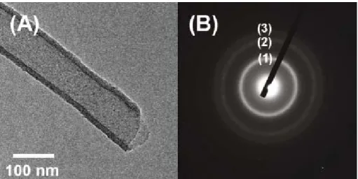
Figure 3.5 TEM studies of a sample grown at 823 K followed by heat treatment at
1273 K. (A) Low magnification image, and (B) SAED.
49
Figure 3.6 Characterization of a sample grown on Si wafer at 773 K followed by
heat treatment at 1273 K. (A) Low magnification SEM image, (B) high magnification image of tube ends, and EDX (inset), (C) TEM image and EDX (inset), and (D) SAED, the polycrystalline diffraction rings are assigned to β-SiC.
49
Figure 3.7 TEM studies of a sample grown at 923 K followed by heat treatment at
1273 K. (A) Low magnification image and EDX (inset, from the squared area). (B) SAED, (C) High-resolution image enlarged from a selected area in A.
50
Figure 3.8 (A) TEM image of a sample grown at 873 K followed by heat treatment
at 1273 K showing a tube end. (B) TEM image, (C) EDX, and (D) ED pattern of a sample grown at 923 K followed by heat treatment at 1273 K still retaining the CaCl2 core.
52
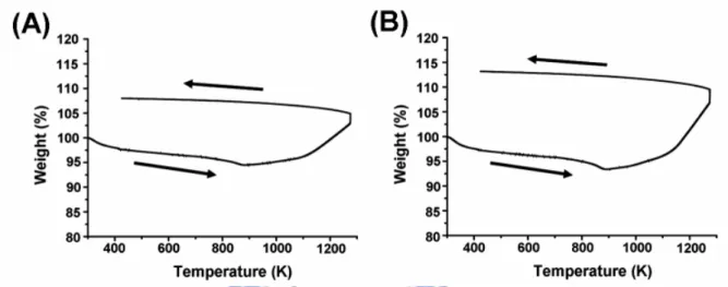
Figure 3.9 TGA of (A) a sample grown at 923 K followed by heat treatment at 1273
K, (B) a sample grown at 823 K followed by heat treatment at 1273 K.
53
Figure 3.10 Field emission J-E curve and Fowler-Nordheim (FN) plot (inset). (A) a
tubular SiC material on Si(100) at 873 K and heat treated at 1273 K. (B) a tubular SiC material on Si(100) at 923 K and heat treated at 1273 K.
57
Chapter 4
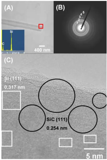
Figure 4.1 SEM images the yellow product prepared from Mg and MeSiHCl2 (A)
Low-magnification, (B) and (C)High-magnification, and (D) EDX
Figure 4.2 TEM images of yellow product prepared from Mg and MeSiHCl2 (A)
and (B) Low-magnification TEM image and SAED inset in (B), (C) HRTEM image of particle from the red square in part (B), and (D) HRTEM image of thin plate, black circle in part (B).
68
Figure 4.3 FT-IR spectrum of the yellow product prepared from Mg and MeSiHCl2.
The absorption bands marked with “*” are from absorbed H2O
molecules.
69
Figure 4.4 XRD partten of the yellow product prepared from Mg and MeSiHCl2.
The peaks marked with “*” are from the XRD holder.
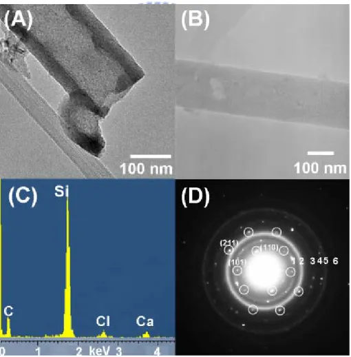
70
Figure 4.5 Characterizations of black product prepared from Mg and Me2SiCl2. (A)
Low-magnification SEM image, (B) high-magnification SEM image and EDX (inset), (C) and (D) low-magnification TEM images, (E) SAED, and (F) HRTEM image.
71
Figure 4.6 XRD partten of the black product prepared from Mg and Me2SiCl2.
71
Figure 4.7 Bulk morphology of (A) NaCl, and (B) MgCl2. 73
Chapter 5
Figure 5.1 MOCVD reactor setup. 79
Figure 5.2 Images of thin films deposited on wafers placed at (A) 40 cm (position
1), (B) 35 cm (position 2), (C) 30 cm (position 3), (D) 25 cm (position 4), (E) 20 cm (position 5), (F) 15 cm (position 6), (G) 10 cm (position 7), (H) 5 cm (position 8), and (I) 0 cm (position 9) away from the center of the furnace.
80
Figure 5.3 Thickness distributions of the samples in the reactor. 81
Figure 5.4 EPMA atomic % concentration of the samples grown from Sn(SiMe3)4 at
923 K, H2 flow rate 20 sccm, and 26.7 Pa.
Figure 5.5 (A) SEM, EDX (inset), and (B) XRD pattern of I. I was grown from
Sn(SiMe3)4 at 923 K, H2 flow rate 20 sccm, and 26.7 Pa.
83
Figure 5.6 XPS spectra of I, grown from Sn(SiMe3)4 at 923 K, H2 flow rate 20
sccm, and 26.7 Pa, as received. (A) Survey and (B) high resolution spectra.
84
Figure 5.7 XPS spectra of I after Ar+ sputtering for 90 s. (A) Survey and (B) high
resolution spectra.
84
Figure 5.8 (A) Raman spectrum of I, grown from Sn(SiMe3)4 at 923 K, H2 flow rate
20 sccm, and 26.7 Pa. (B) curve fitting of (A).
85
Figure 5.9 SEM and EDX of I-P, prepared by treating I with H2 plasma at 923 K.
(A) Low and (B) high magnification image, EDX of (C) black circle and (D) red sequare in (B).
86
Figure 5.10 (A) SEM and (B) EDX of I-P-HF, prepared by treating I with H2
plasma at 923 K followed by etching in HF(aq) at 298 K.
87
Figure 5.11 (A) SEM, (B) EDX, (C) cross-sectional SEM, and (D) TEM and ED
(inset) of II, obtained by annealing I-P-HF at 1273 K under vacuum.
87
Figure 5.12 FT-IR spectra of (A) I, grown from Sn(SiMe3)4 at 923 K, H2 flow rate
20 sccm, and 26.7 Pa; (B) I-P, prepared by treating I with H2 plasma at
923 K; (C) I-P-HF, obtained by etching I-P in HF(aq) at 298 K; and (D)
II, obtained by annealing I-P-HF at 1273 K under vacuum.
88
Figure 5.13 (A) SEM, (B) EDX, (C) cross-sectional SEM, (D) low magnification
TEM, (E) SAED, and (F) HRTEM from the red-square area in (D) of
III, obtained by annealing I-P at 1423 K under vacuum.
90
Figure 5.14 XRD of III, obtained by annealing I-P at 1423 K under vacuum. (The
peak marked with “*” is from the sample holder.)
Figure 5.15 I-V characters of (A) I, grown from Sn(SiMe3)4 at 923 K, H2 flow rate
20 sccm, and 26.7 Pa; (B) I-P annealed at 1073 K, prepared by treating
I with H2 plasma at 923 K and annealed at 1073 K; and (C) III,
obtained by annealing I-P at 1423 K under vacuum.
92
Figure 5.16 I-V characters of (A) IV/p-type Si junction and (B) P doped-IV/p-type
Si junction. IV was prepared by annealing I (grown for only 90 min) at 1423 K under vacuum for 1 h.
93
Figure 5.17 SIMS depth profile of IV, obtained by annealing I (grown for only 90
min) at 1423 K under vacuum. (The thin film-substrate interface is proposed to be at 0.6 – 0.8 μm, starting at the red line.)
93
Figure 5.18 GC-MS traces of volatile byproducts trapped at 77 K. The peaks are
identified to be (A) air, (B) Me3SiH, (C) Me6Si2, and (D) [Me2SiCH2]2.
(The peak marked with “*” are unidentified.)
94
Chapter 6
Figure 6.1 Characterization of the dark green thin films reacted with HAuCl4 in the
CTAC solution.(A) low-magnification SEM image, and EDX (inset) (B) high- magnification SEM image (C) low magnification TEM image and SAED (inset) (D) high resolution TEM image (E) XRD partten, and (F) plot of current-voltage (I-V) curve of a gold nanowire.
104
Chapter 7
Figure 7.1 SiC nanostructures obtained in this study from self-templating methods. 110
Figure 7.2 Summarized the results from Sn nanoparticles embedded in amorphous
SixC1-x thin films via Sn(SiMe3)4 as MOCVD precursor.
110
Figure 7.3 Summarized the possible applications of the materials fabricated in this
study.
Chapter 1
Introduction
1.1 Introduction
Silicon and silicon-based materials have played an important role in the development of modern semiconductor device technology. Today, most of electronic products such as computer, cell phone, and digital audio player are produced by silicon semiconductor. However, silicon carbide (SiC) material has a very high breakdown field (3-5 MV/cm), typically 8-10 times higher than that for silicon (0.25 MV/cm), and prominent thermal conductivity of silicon carbide (3.2-4.9 Wm-1K-1) is 2-3 times higher than that for silicon (1.5
Wm-1K-1).1 In addition, its excellent strength, hardness, and resistance to oxidation and
thermal shock, SiC has more potential for application in harsh operation environments than widely utilized silicon devices.2-4 Owing to these superior properties, lots of scientists are
devoted to develop silicon carbide material in the last 100 years.
Recently, it is known that size of materials within the nanometer regime might have unique properties associated with their morphology and size. Nanostructured SiC could be a highly functional material.5 For instance, Wong et al. showed that the elasticity and strength
of SiC nanorod were greater than those of bulk SiC in a study of nanobeam mechanism.6
In this dissertation, we will reveal different types of SiC nanostructures, such as SiC nanoparticles, SiC nanocages, pseudo thin plate SiC nanostructures, tubular SiC nanostructures, and porous SiC thin films that can be fabricated based on the phase segregation concept. SiC nanostructures have very special properties which bode well for applications in blue light emitters, field emission display, hydrogen storage, photocatalytic and nanoscal electro-devices. In our study, potential application of tubular SiC as an efficient
field emitting material and fabrication of n-type porous SiC thin films on p-type silicon wafer to produce a heterjunction diode will be explored.
1.2 Structure and Properties of SiC
1.2.1 Structure of SiC
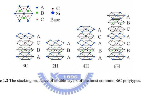
SiC belongs to IV-IV semiconductors and there exist more than 130 polytypes.7 All
polytypes have a hexagonal frame with a carbon atom located above the center of a triangle of Si atoms and under a Si atom belonging to the next layer as shown in Figure 1.1.8
Figure 1.1 The unit cell of 3C-SiC. The distance, a, between neighboring silicon, and C-Si are
approximately 0.308 nm, and 0.189 nm, respectively.
The distance, a, between neighboring silicon or carbon atoms is approximately 0.308 nm for all polytypes.9 The carbon atom is positioned at the center of mass of the tetrahedral structure
outlined by four neighboring Si atoms so that the distance between the C atom to each of the Si atoms is the same. Geometrical considerations give that this distance, C-Si, is (3/8)1/2a i.e.
approximately equal to 0.189 nm. The polytypes of SiC differ from one another only in the stacking sequence of double layers of silicon and carbon atoms. The stacking direction is the c-axis in the hexagonal frame of reference.
The stacking sequence is shown for the most common polytypes, 3C, 2H, 4H and 6H in Figure 1.2. If the first double layer is called the A position, the next layer that can be placed
according to a closed packed structure will be placed on the B position or the C position. The different polytypes will be constructed by permutations of these three positions. For example, 3C-SiC will have a stacking sequence ABC while the number is the number of double layers in a stacking repeating sequence and the letter represents crystal structure which in this case is cubic. The only cubic form 3C-SiC sometimes referred to as β-SiC. If the double layers have
Figure 1.2 The stacking sequence of double layers of the most common SiC polytypes.8
the same adjoining position, they have a 6-fold symetyaxis and crystallize into a hexagonal phase product. For example, 2H-SiC have a stacking sequence AB with a hexagonal structure. Other possibilities are ABAC, called 4H, and ABCACB, called 6H. All of hexagonal (H) or rhombohedral (R) polytypes expect cubic phase are commonly referred to as α−SiC. The crystal structure of 3C-SiC corresponds to cubic ZnS (zinc blende phase) and 2Η, 4Η, and 6Η-SiC are hexagonal ZnS wurtzite phase.
1.2.2 Properties of SiC
The color of 3C-SiC is yellow while 6Η−SiC is colorless. The different polytypes of SiC have wide energy band gaps at room temperature from 2.2 eV for 3C-SiC, 2.9 eV for 6H-SiC
to 3.4 eV for 4H-SiC. The bandgaps at liquid helium temperature are 2.4 eV for 3C-SiC, 3.2 eV for 4H-SiC, 3.0 for 6H-SiC. 8,10,11,12 The other physical properties for most common types
3C, 4H, and 6H-SiC are summarized in Table 1.1.
Table 1.1 Physical properties of the most common SiC polytypes. 8,10,11,12
3C-SiC 4H-SiC 6H-SiC
Bandgap (eV) at 5K 2.4 3.2 3.0
Space group F4 3m P63mc P63mc
Lattice a (nm) 0.436 0.308 0.308
Lattice c (nm) 0.436 1.008 1.512
Si-C Bond length (nm) 0.189 0.189 0.189
Density (g/cm3) 3.2 3.2 3.2
Melting point (K) 3103 3103 3103
Mohs hardness 9.0 9.0 9.0
In addition, we also show some important device parameters in terms of electric properties of most common types 3C, and 6H-SiC and other common semiconductors in Table 1.2. The maxium operating temperature for Si is 573 K, but for SiC, it is above 873 K. Below 1773 K, SiC is stable in an oxidizing atmosphere. This gives it an edge over diamond. Long term stability at high temperatures is a problem for III-V compounds, such as GaAs and GaP. These are reasons why SiC is considered as a good candidate for semiconductor device applications.
Table 1.2 Electric properties of SiC and other semiconductors. 8,10,11,12
Unit Si GaAs 3C-SiC 6H-SiC Diamond
Bandgap at 5 K eV 1.12 1.43 2.4 3.0 5.6 Electron mobility (R.T.) cm2/V⋅s 1350 8500 1000 500 2200 Hole mobility (R.T.) cm2/V⋅s 480 400 40 80 1600
Breakdown voltage 106 V/cm 0.3 0.4 4 4 10
Thermal conductivity W/cm⋅K 1.5 0.5 5.0 5.0 20.0 Sat. elec. drift. vel. 107 V/s 1.0 1.0 2.5 2.0 2.7
1.3 Synthetic Methods of SiC
The conventional processes for preparation of SiC material are the carbothermic reduction of silica carbon mixture, chemical vapor deposition techniques, and pyrolysis of polycarbosilane precursor. We will discuss more details below. In addition, self-propagating high temperature synthesis (SHS), based on the exothermic reaction between silicon micropowder and active carbon was carried out at ignition temperature of 1523 K - 1923 K.13,14 Reduction-carbonization route, in which was carried out in autoclave using metallic Na
as the reluctant, SiCl4 and carbon, CClx as source materials at 873 K - 923 K.15,16 Na flux
method by a mixture of silicon and fullerene powders were heating at 700 K- 1000 K in a sodium melt, and various other methods such as sol-gel, plasma, microwave radiation technologies have also been reported. 17-22
In 1966, Klinger et al. studied the carbothermic reduction of silica carbon mixture to produce SiC at 1718 K- 2038 K under vacuum, which can be represented below by two equations 1.1-1.2.
The reaction could proceed via the gas phase by dissociation of silica into oxygen and silicon monoxide and subsequent reaction with graphite to form vapor phase carbon monoxide and silicon carbide. 23 This is the most common route to produce SiC powders.
Chemical vapor deposition (CVD) is a single step process, which can deposit SiC material on an arbitrarily shaped substrate.24,25 Most works use a silicon-containing and a
carbon-containing gas-phase species, including a combination of SiH4 and CH4,26-29 SiH4 and
C3H8,30,31 and Si2H6 and C2H2.32 For example, the SiH4-C3H8-H2 system, it is postulated that
the following sequence of steps leads to the SiC.33
Here X denotes the active substrate site, and D.X denotes the species D in the adsorbed state. The Ki’s are equilibrium constants and Kr is the reaction rate constant for the bimolecular
surface reaction Eqn. (1.7). At the beginning, SiH4 and C3H8 decomposed in the gas phase to
form SiH2, H2, CH4, and C2H2 at high reaction temperature. Gas species of SiH2 and CH4
were absorbed on the active substrate site and reacted with each other to form SiC on the surface of the substrate.
Organochlorosilicon compounds, dichlorodimethylsilane (Me2SiCl2), 34,35
trichloromethylsilane (MeSiCl3),36,37 were used as single-source CVD precursors the
organochlorosilane molecules first decomposed in the gas phase at high temperature 1273 K- 1573 K in H2 atmosphere to form intermediate species containing silicon and/or carbon atoms,
hexmethyldisilane (HMDS), 1,1-dimethyl-1-silacyclobutabe, tetrakis(trimethylsilyl)silane (TMSS), and dodecamethylcyclohexasilane also acted as single-source CVD precursors. They decomposed into H2SiMe2, HSiMe3, Si2Me6, and [Me2SiCH2] at lower reaction temperature to
form ceramic precursor layers. These were converted into crystalline SiC thin film by heat treatment above 1273 K.38-41
In general, CVD is a complicated process that includes (i) mass and energy transfer in the gas phase and (ii) gas-phase and surface chemical reaction. Film-growth species are sensitive to the reactor geometry and operating conditions. Therefore, it is necessary to design the CVD process and to choose suitable operating conditions.
In 1975, Yajima and his co-workers were the first successful in fabricating silicon carbide from preceramic organosilicon polymers.42,43 The synthetic method is shown in
equation 1.8. Metallic lithium was allowed to dechlorinate dimemethyldichlorosilane to
produce dodecamethylcyclohexasilane. The dodecamethylcyclohexasilane was purified by means of recrystallization and sublimation. It was heated at 673 K for 48 h in autoclave to produce polycarbosilane. After heat-treatment at 1773 K under vacuum, polycarbosilane converted into SiC. This is a complicated, expensive, and time-consuming method. In 1976, Yajima and co-workers improved the above method by replacing lithium with sodium as shown in equation 1.9.44-49 The Me2SiCl2 was dechloroinated by the molten sodium, resulting
polysilane was removed by filitration and then heated at at 743 K for 5 h in argon gas atmosphere to form polycarbosilane. After heat-treatment at 1573 K under vacuum, the
polycarbosilane converted into SiC. This synthetic method of polycarbonsilane is very simpler and more economical.
According to this process, Bianconi and her co-workers fabricated a netwok polymer polysilane, [RSi]n. They used n-hexylSiCl3 instead of Me2SiCl2 to react with metallic
sodium/potassium (1:1) alloy in pentane solution. Pyrolysis of the netwokpolymer formed SiC with some Si.50,51 In 1992, Seyfer’s group also reported various partially linear and partially
network precramic polymers, [(MeSiH)x(MeSi)1-x]n, converted them into SiC with some Si
follow by annealed at 1773 K .52-54
In this dissertation, we extend on the pyrolysis of polycarbosilane process to produce SiC. We simplified the Yajima process, using organochlorosilanes to react with metallic sodium, magnesium, and calcium in solvent-free condition at 523 K - 923 K. Then the products were converted into SiC nanostructure after heat treatment at 1273 K under vacuum. Besides, we also fabricated porous SiC thin films on Si substrate using a single-source precursor, Sn(SiMe3)4, by CVD process.
1.4 Nanostructures of SiC
1.4.1 SiC Nanocrystals
reduction of silica, reduction-carbonization route, plasma, microwave radiation techniques and various chemical vapor deposition methods.15-17,20,21,23 Recently, aqueous suspensions of
3C-SiC nanocrystals with a diameter 1-6 nm showing intense emission have been successfully fabricated by dispersing electrochemically etched porous polycrystalline 3C-SiC wafers in different solvents (water, ethanol, toluene).55-56 The photoluminescence (PL) spectra exhibited
continuous redshifts with increasing excitation wavelength and provides clear evidence of quantum confinement.57-58 Based on this method, 3C-SiC/polystyrene composite films that
luminescence in blue region have also been reported.59 Thermal SiO2 thin films have been
implanted Si and C to produce SiC nanocrystals embedded in SiO2 matrix can also exhibit PL
emission. The origins of the luminescence were suggested to relate to defects in the silicon oxide at the SiC/SiO2 interface, amorphous carbon clusters, or SiC grains. 60-64 Therefore, SiC
nanocrystals have potential to be applied in blue light emitters in displays. Combined with their excellent biocompatibity, especially in blood, low density, and high rigidity SiC nanocrystals are potentially usefulin biology and medicine as well.65,66
1.4.2 One-Dimensional SiC Nanostructures
One dimensional (1D) nanostructures such as rods, wires, belts, and tubes have been attracted much attention due to their unique application in mesoscopic physics and fabrication of nanoscale devices.67-70 SiC 1D nanostructures have shown many outstanding performance
because of their excellent properties. It can be used in field emission display, hydrogen storage, photocatalytic and nanoscal electro-devices.71-73 Thus, many researchers have
searched for methods to synthesize 1D SiC nanostructures in the last few years. 1D nanomaterials contains solid nanorods, nanowires, and hollow nanotubes. Below, we will divide into two sections to discuss some general methods to produce 1D SiC nanostructures.
1.4.2-1.1 SiC Nanorod and Nanowires from Hard Template Methods
Since the discovery of carbon nanotubes by Iijima in 1991,74 most of outstanding
mechanical or electrical properties have been known in last few years.75-76 They show
promises in a wide variety of applications, including chemical sensors, field emitter, interconnects, and scanning probe.77-80 In addition, carbon nanotubes open up new and
exciting possibilities for making different kinds of nanosized heterostructures by filling the inside hollow space with other elements or by decorating the outside surfaces of the nanotubes. For example, various metal naowires, gallium nitride nanowires, and Si-B-C-N nanocable, have been synthesized using carbon nanotubes as templates.81-83 These fabrication
methods highly promising because of the morphological integrity of carbon nanotubes, which can spatially confine the reaction inside the nanotubes. The net result is the formation of one-dimensional products with diameters, lengths, and orientations similar to those the carbon nanotubes templates.
Carbon nanotube can act not only as a template but also as a reactant to produce 1D SiC material. Dai et al. successfully prepared SiC nanorods through a reaction between carbon nanotubes and SiO or SiI2.84 Pan et al. also fabricated SiC nanowires by using high aspect
ratio aligned carbon nanotubes to react with SiO at 1673 K.85
1.4.2-1.2 SiC Nanorod and Nanowires from Vapor-Liquid-Solid Methods
The growth of one-dimensional nanostructures via a gas phase reaction involving the vapor-liquid-solid (VLS) process has been widely studied. This process was originally developed by Wagner and co-workers to produce micrometer-sized whiskers in 1960s.86
Recently, many research groups can generate nanowires and nanorods for a rich variety of inorganic materials.87-90 The VLS process starts with the dissolution of gaseous reactants into
nanosized liquid droplets of a catalyst metal. The saturated component would undergo nucleation, crystallization, and growth into rods and then wires. The 1D growth is mainly
induced and dictated by the liquid droplets of catalyst metal. Assuming that the size of the catalyze does not change during the wire growth, and the diameter of wire will be controlled by the liquid droplets of the catalyst metal. Wu et al. and co-workers have demonstrated the validity of VLS at nanometer scale by real-time observation of Ge nanowire growth in an high-temperature transmission electron microscopic (TEM).91 Moreover, Bando’s group
effectively fabricated core-shell heterostructure SiC@BN, and SiC-SiO2-C nanocable by VLS
method.92-93
1.4.2-1.3 SiC Nanorod and Nanowires from Vapor-Solid Methods
The vapor-solid (VS) method, without any metal catalysts for whisker growth, also holds for the growth of 1D nanomaterials.94 In this process, evaporation, chemical reduction or
gaseous reaction first generates the vapor. The vapor is gradually transported and condensed onto a substrate. Thus, it leads to the growth of 1D nanostructure. The supersaturation ratio of condensing species in the gas plays a key role. To enable anisotropic growth to form nanowires, the supersaturation ratio of condensing species must be controlled carefully otherwise, two-dimensional and isotropic growths would occur.95,96
Recently, our group reported that addition of poly(dimethylsiloxane) to a solvent-free vapor-solid reaction growth (VSRG) process assisted Cu nanowire formation significantly.97
A simple high yield synthesis Ag nanowires which is carried out by using AgNO3 and
(Me3Si)4Si were prepared in a sealed tube under low pressure at 400 K. The key step in this
preparation is the in situ generation of a silica shell layer.98 In VSRG, the reaction takes place
at the vapor-solid interface, which is the surface of solid reactant. Phase separated solid product may develop into core-shell nanowires when the conditions are suitable. In additional, we also fabricated CaF2@C and MgF2@C core-shell 1D heterostructures through VSRG
1.4.2-2 Tubular SiC
Tubular 1 D materials such as carbon nanotube, vanadium oxide nanotube, and tungsten sulfide nanotube are caused by the transformation from curing the layered nanoparticles (2D) into nanotube (1D) in structure phase due to reduce the dangling bond at the edge of the plane when they are in nanometer size regime. 74,100,101 Other materials with normal crystal structure
are difficult to form hollow nanotubes. Therefore, there were little reports on the synthesis of tubular silicon carbide 1 D nanostructures. Hu et al., Zhou et al., and Sun et al. used hard-template-assisted method to produce SiC nanotube. Drawbacks of these approaches include low yields, low crystalline, and difficulty to remove extra-templates. 102-104 It will be a
challenge to produce a high yields tubular silicon carbide through a simple method.
1.4.3 Porous SiC Nanostructure
Because of its potential usefulness for luminescence and sensing devices, porous silicon carbide thin film on SiC or Si also have been attracted much attention in recent years. Electrochemical etching of bulk silicon carbide substrates in HF solution, which the same process is used to form porous Si is the only method to fabricate it into the porous form onto SiC and Si wafers .105-107 However, the route of electrochemical etching is not suitable for the
fabrication of porous SiC thin films onto Si substrates. This is due to the high reactivity of Si towards the HF electrolyte, which would cause preferential dissolution of the Si substrate.108
But porous SiC powders prepared via nanocasting and carbothermal reduction process have been reported.109,110 Porous SiC powders are not easy to transform into thin films for
electronic devices. In addition, it is difficult to produce non-oxide ceramic porous materials via sol-gel process.111 Thus, it is a challenging issue to develop a new process to fabricate
1.5 Goal of This Thesis
In this thesis, we simplify Yajima process via vapor-liquid or vapor-solid reaction in solvent-free conditions to fabricate SiC nanostructures based on the phase segregation concept. This is a new and simple method to fabricate various SiC nanostructures easily.
We employ various organochlorosilanes react with active metals Na, Ca, and Mg to form preceramic precursor and salt products. The salts work as templates to assist the structure formation. Spherical and nanocages of SiC are formed via the ceramic precursor and the byproduct NaCl. One dimensional SiC nanotubes are successful developed from the precursor and CaCl2. From the byproduct, MgCl2, and the precursor, pseudo thin plate SiC
nanostructure can be prepared also.
In addition, we extend the phase segregation concept to grow porous β-SiC thin film onto silicon wafer. Using Sn(SiMe3)4 as the single-source precursor for metal-organic
chemical vapor deposition (MOCVD). SiC thin film with embedded Sn nanoparticles can be grown. The metal Sn particles act as in situ generated templates to assist the formation of porous SiC thin films.
The detail experimental conditions of these results will be discussed in the following chapters.
1.6 References
(1) Casady, J. B.; Johnson, R. W. Solid-State Electron. 1996, 39, 1409.
(2) Niihara, K. Ceram. Bull. 1984, 63,1160.
(3) Narushima, T.; Goto, T.; Lguchi, Y.; Hirai, T. J. Am. Ceram. Soc. 1990, 73, 3580.
(4) Spetz, A. L.; Baranzani, A.; Tobias, P.; Lundström, I. Phys. Stat. Sol. (a) 1997, 162, 493. (5) Devaty R. P.; Choyke W. J. Phys Stat Sol (a) 1997, 162, 5.
(6) Wong, E. W.; Sheehan, P. E.; Lieber, C. M. Science 1997, 277, 1971.
(7) Verma, A. R.; Krishna, P. Polymorphism and Polytypism in Crystals, Wiley, New York,
1966, Chapter 5, p 92.
(8) http://www.ifm.liu.se/matephys/new_page/research/sic/ (9) Knippenberg, W. F. Philips Research Reports, 1963, 18, 161.
(10) Harris, G. L.; Yang, C. Y.-W. Amorphous and Crystalline Silicon Carbide, 1987, Part I, p 3.
(11) Harris, G. L. Properties of Silicon Carbide, Inspec, U.K., 1995, Chapter 2, p 31.
(12) Zetterling, C.-M. Process Technology for Silicon Carbide Devices, Inspec, U.K., 2002, Chapter 2, p 4.
(13) Pampuch, R.; Stobierski, L.; Lis, J.; Raczka, M. Mater. Res. Bull. 1987, 22, 1225.
(14) Narayan, J.; Raghunathan, R.; Chowdhury, R.; Jagannadham, K. J. Appl. Phys. 1994, 75, 7252.
(15) Hu, J.-Q.; Lu, Q.-Y.; Tang, K.-B. ; Qian, Y.-T. ; Zhou, G.-E. ; Liu, X.-M. ; Wu, J.-X. Chem. Mater. 1999, 11, 2369.
(16) Shen, G.-Z ; Chen, D. ; Tang, K.B. ; Qian, Y.-T. ; Zhang, S.-Y. Chem.Phys. Lett. 2003, 375, 177.
(17) Kawamura, F.; Yamane, H.; Yamada, T.; Yin, S.; Sato, T. J. Ceram. Soc. Jpn. 2007, 115, 74.
(19) Seog, I. S.; Kim, C. H. J. Mater. Sci. 1993, 28, 3227.
(20) Zhu, W.; Zhao, G. Y.; Revankaar, V.; Hlavacek, V. J. Mater. Sci. 1993, 28, 659. (21) Guo, J. Y.; Gitzhofer, F.; Boulos, M. I. J. Mater. Sci. 1995, 30, 5589.
(22) Ramesh, P. D.; Vaidhyanathan, B.; Ganguli, M.; Rao, R. J. J. Mater. Res. 1994, 9, 3025. (23) Klinger, N. ; Strauss, E. L. ; Komarek K. L. J. Am. Ceram. Soc. 1966, 49, 369.
(24) Schlichting, J. Powder Metal. Int. 1980, 12, 141.
(25) Fischman, G. S.; Petuskey, W. T. J. Am. Ceram. Soc. 1985, 68, 185.
(26) Tabata, A.; Nakajima, T.; Mizutani, T.; Suzuoki, Y. Jpn. J. Appl. Phys.2003,42 10. (27) Schroder, B.; Holger, U.; Lederman, A.; Mukherjee, C. Thin Solid Films 2001, 395, 298. (28) Itoh, T.; Fujiwara, T.; Katoh, Y.; Fukunaga, K.; Nonomura, S. J. Non-Cryst. Solids 2002,
299–302, 880.
(29) Yu, Rusli, M. B.; Yoon, S. F.; Chen, Z. M.; Ann, J.; Zhang, Q.; Chew, K.; Cui, J. J. Appl. Phys. 2000, 87, 8155.
(30) Nishino, S.; Suhara, H.; Ono, H.; Matsunami, H. J. Appl. Phys. 1987, 61, 4889. (31) Allendorf, M. D.; Kee, H. J. J. Electrochem. Soc. 1991, 138, 841.
(32) Hong, L.-S.; Shimogaki, V.; Egashira, V.; Komiyama, H. J. Electrochem. Soc. 1992, 139, 3652.
(33) Harris, G. L.; Yang, C. Y.-W. Amorphous and Crystalline Silicon Carbide, 1987, Part I, p 51.
(34) Takeuchi, T.; Egashira, Y.; Osawa, T.; Komiyama, H. J. Electrochem. Soc. 1998, 145, 1277.
(35) Chen, L.; Goto, T.; Hirai, T. J. Mater. Sci. 1990, 25, 4614. (36) Choi, B. J.; Kin, D. R. J. Mater. Sci. Lett. 1991, 10, 860.
(37) Fu, Q.-G. ; Li, H.-J. ; Shi, X.-H.; Li, K.-Z.; Wei, J.; Hu, Z.-B. Mater. Chem. Phys. 2006, 100, 108.
(39) Chiu, H.-T.; Hsu, J.-S. Thin Solid Films 1994, 252, 13.
(40) (a) Chiu, H.-T.; Lee, S.-F. J. Chin. Chem. Soc. 1992, 39, 239. (b) Chiu, H.-T.; Lee, S.-F. J. Mater. Sci. Lett. 1991, 10, 1323. (c) Chiu, H.-T.; Wu, P.-F. J. Chin. Chem. Soc. 1991, 38, 231.
(41) (a) Wróbel, A. M.; Wickramanayaka, S.; Nakanishi, Y.; Hatanaka, Y.; Pawłowski, S.; Olejniczak, W. Diamond Relat. Mater. 1997, 6, 1081. (b) Wróbel, A. M.; Walkiewicz-Pietrzykowska, A. Chem. Vap. Deposition 1998, 4, 133.
(42) Yajima, S.; Hayashi, J.; Omori, M. Chem. Lett. 1975, 931. (43) Yajima, S.; Okamura, K.; Hayashi, J. Chem. Lett. 1975, 1209.
(44) Yajima, S.; Omori, M.; Hayashi, J.; Okamura, K.; Matsuzawa, T.; Liaw, C.-F. Chem. Lett. 1976, 551.
(45) Yajima, S.; Hayashi, J.; Omori, M.; Okamura, K. Nature 1976, 261, 683.
(46) Yajima, S.; Hayasht, J.; Hasegawa, Y.; Iimura, M. J. Mater. Sci. 1978, 13, 2569. (47) Hasegawa, Y.; Iimura, M.; Yajima, S. J. Mater. Sci. 1980, 15, 720.
(48) Hasegawa, Y.; Okamura, K. J. Mater. Sci. 1983, 18, 3633.
(49) Ichikawa, H; Machino, F.; Mitsuno, S.; Ishikawa, T.; Okamura, K.; Hasegawa, Y. J. Mater. Sci. 1986, 21, 4352.
(50) Bianconi, P. A.; Weidman, T. W. J. Am. Chem. Soc. 1988, 110, 2342.
(51) Bianconi, P. A.; Schilling, F. C.; Weidman, T. W. Macromolecules 1989, 22, 1697. (52) Seyferth, D.; Wood, T. G.; Tracy, H. J.; Robison, J. I. J. Am. Ceram. Soc. 1992, 75, 1300. (53) Seyferth, D.; Lang, H. Organometallics 1991, 10, 551.
(54) Czubarow, P.; Sugimoto, T.; Seyferth, D. Macromolecules 1998, 31, 229.
(55) Wu, X. L.; Fan, J. Y.; Qiu, T.; Yang, X.; Siu, G. G.; Chu, P. K. Phys. Rev. Lett. 2005, 94, 26102.
(57) Efros, Al. L.; Efros, A. L.; Sov. Phys. Semicond. 1982, 16, 772. (58) Brus, L. J. Chem. Phys. 1983, 79, 5566.
(59) Fan, J. Y.; Wu, X. L.; Kong, F.; Qiu, T.; Huang, G. S. Appl. Phys. Lett. 2005, 86, 171903.
(60) Fan, J. Y.; Wu, X. L.; Chu, P. K. Prog. Mater. Sci. 2006, 51, 983.
(61) Zhao, J.; Mao, D.S.; Lin, Z.X.; Jiang, B.Y.; Yu, Y.H.; Liu, X. H.; Wang, H. Z.; Yang, G. Q. Appl Phys Lett 1998, 73, 1838.
(62) Pérez-Rodríguez, A.; González-Varona, O.; Garrido, B.; Pellegrino, P.; Morante, J. R.; Bonafos, C.; Carrada, M.; Claverie, A. J. Appl. Phys. 2003, 94, 254.
(63) Chen, D.; Liao, Z. M.; Wang, L.; Wang, H. Z.; Zhao, F.; Cheung, W. Y. Opt. Mater.
2003, 23, 65.
(64) An, Z.; Fu, R. K. Y.; Chen, P.; Liu, W.; Chu, P. K.; Lin, C. J. Vac. Sci. Technol. B 2003, 21, 1375.
(65) Chan, W. C. W.; Nie, S. Science 1998, 281, 2016.
(66) Bruchez, J. M.; Moronne, M.; Gin, P.; Weiss, S.; Alivisatos, A. P. Science 1998, 281, 2013.
(67) Wang, Z. L. Adv. Mater. 2000, 12, 1295.
(68) Xia, Y.; Yang, P.; Sun, Y.; Wu, Y.; Mayers, B.; Gates, B.; Yin, Y.; Kim, F.; Yan, H. Adv. Mater. 2003, 15, 353.
(69) Hu, J.; Odom, T. W.; Liber, C. M. Acc. Chem. Res. 1999, 32, 435.
(70) Rao, C. N. R.; Deepak, F. L.; Gundiah, G.; Govindaraj, A. Prog. Solid State Chem. 2003, 31, 5.
(71) Lo, H. C.; Das, D.; Hwang, J. S.; Chen, K. H.; Hsn, C. H.; Chen, C. F.; Chen, L. C. Appl. Phys. Lett. 2003, 83, 1420.
(72) Mpourmpakis, G.; Froudakis, G. E. ; Lithoxoos, G. P.; Samios, J. Nano Lett. 2006, 6, 1581.
(73) Zhou, W.; Yan, L.; Wang, Y.; Zhang, Y. Appl. Phys. Lett. 2006, 89, 013105. (74) Iijima, S. Nature 1991, 354, 56.
(75) Hone, J.; Batlogg, B.; Benes, Z.; Johnson, A. T.; Fischer, J. E. Science 2000, 289, 1730. (76) Yu, M. F.; Files, B. S. ; Arepalli, S. ; Ruoff, R. S. Phys. Rev. Lett. 2000, 84, 5552. (77) Li, J.; Lu, Y.; Ye, Q.; Cinke, M.; Han, J.; Meyyappan, M. Nano Lett. 2003, 3, 929.
(78) Cassell, A. M.; Ye, Q.; Cruden, B. A. ; Li, J. ; Sarrazin, P. C.; Ng, H. T.; Han, J.; Meyyappan, M. Nanotechnol. 2004, 15, 9.
(79) Li, J.; Ng, H. T.; Cassell, A. M.; Fan, W.; Chen, H.; Ye, Q.; Koehne, J.; Han, J.; Meyyappan, M. Nano Lett. 2003, 3, 597.
(80) Dai, H.; Hafner, J. H.; Rinzler, A. G.; Colbert, D. T.; Smalley, R. E. Nature 1996, 384, 147.
(81) Guerretpiecout, C.; Lebouar, Y.; Loiseau, A.; Pascard, H. Nature, 1994, 372, 761. (82) Han, W. Q. ; Fan, S. S. ; Li, Q. Q.; Hu, Y. D. Science, 1997, 277, 1287.
(83) Zhang, Y.; Suenaga, K.; Colliex, C.; Iijima, S. Science 1998, 281, 973.
(84) Dai, H. J.; Wong, E. W. ; Lu, Y. Z.; Fan, S. S.; Lieber, C. M. Nature 1995, 375, 769. (85) Pan, Z. W.; Lai, H. L.; Au, F. C. K.; Duan, X. F.; Zhou, W. Y.; Shi, W. S.; Wang, N.; Lee,
C. S.; Wong, N. B.; Lee, S. T.; Xie, S. S. Adv. Mater. 2000, 12, 1186. (86) Wagner, R. S.; Ellis, W. C. Appl. Phys. Lett. 1964, 4, 89.
(87) Duan, X. ; Liber, C. M. Adv. Mater. 2000, 12, 298. (88) Wu, Y.; Yang, P. Chem. Mater. 2000, 12, 605.
(89) Chen, C.-C.; Yeh, C.-C.; Chen, C.-H.; Yu, M.-Y.; Liu, H.-L.; Wu, J.-J.; Chen, K.-H.; Chen, L.-C.; Peng, J.-Y.; Chen, Y.-F. J. Am. Chem. Soc. 2001, 123, 2791.
(90) Huang, M. H.; Wu, Y.; Feick, H. J.; Tran, N.; Weber, E.; Yang, P. Adv. Mater. 2001, 13, 113.
(91) Wu, Y.; Yang, P. J. Am. Chem. Soc. 2001, 123, 3165.
Phys. Lett. 2002, 80, 4641.
(93) Li, Y.; Bando, Y; Golberg, D. Adv. Mater. 2004, 16, 93.
(94) Levitt, A. P. Whisker Technology, Wiley-Interscience, New York 1970. (95) Hsu, Y.-J; Lu, S.-Y. J. Phys. Chem. B 2005, 109, 4398.
(96) Wang, Y.; Zhang, L.; Meng, G.; Liang, C.; Wang, G.; Sun, S. Chem. Commun. 2001, 2632.
(97) Yen, M.-Y.; Chiu, C.-W.; Shia, C.-H.; Chen, F.-R.; Kai, J.-J.; Lee, C.-Y.; Chiu, H.-T. Adv.Mater. 2003, 15, 235.
(98) Hsia, C.-H.; Yen, M.-Y.; Lin, C.-C.; Chiu, H.-T.; Lee, C.-Y. J. Am. Chem. Soc. 2003, 125, 9940.
(99) Huang, C.-H.; Chang, Y.-H.; Lee, C.-Y.; Chiu, H.-T. Langmuir 2006, 22, 10. (100) Patzke, G. R.; Krumeich, F.; Nesper, R. Angew. Chem. Int. Ed. 2002, 41, 2447.
(101) Rosentsveig, R.; Margolin, A.; Feldman, Y.; Popovitz-Biro, R.; Tenne, R. Chem. Mater.
2002, 14, 471.
(102) Sun, X. H.; Li, C. P.; Wong, W. K.; Wong, N. B.; Lee, C. S.; Lee, S. T.; Teo, B. K. J. Am. Chem. Soc. 2002, 124, 14464.
(103) Hu, J. Q.; Bando, Y.; Zhan, J. H.; Golberg, D. Appl. Phys. Lett. 2004, 85, 2932. (104) Wang, H.; Li, X.-D.; Kim, T.-S.; Kim, D.-P. Appl. Phys. Lett. 2005, 86, 173104.
(105) Matsumoto, T.; Takahashi, J.; Tamaki, T.; Futagi, T.; Mimura, H.; Kanemitus. Y. Appl. Phys. Lett. 1994, 64, 226.
(106) Connolly, E. J.; Timmer, B.; Pham, H. T. M.; Groeneweg, J.; Sarro, P. M.; Olthuis, W.; French, P. J. Sens. Actuators B 2005, 109, 44
(107) Rittenhouse, T. L.; Bohn, P. W.; Hossain, T. K.; Adesida, I.; Lindesay, J.; Marcus, A. J. Appl. Phys. 2004, 95, 490.
(108) Takazawa, A.; Tamura, T.; Yamada, M. Jpn. J. Appl. Phys. 1993, 32, 3148. (109) Krawiec, P.; Geiger, D.; Kaskel, S. Chem. Commun. 2006, 2469.
(110) Sonnenburg, K.; Adelhelm, P.; Antonietti, M.; Smarsly, B.; Nöske, R.; Strauch, P. Phys. Chem. Chem. Phys. 2006, 8, 3561.
(111) Soler-IIIia, G. J. de A. A.; Sanchez, C.; Lebeau, B.; Patarin, J. Chem. Rev. 2002, 102, 4093.
Chapter 2
Silicon Carbide Nanostructures from Reactions between Vapors of
Organochlorosilanes and Liquid of Sodium - Factors Affecting Morphology
and Composition
2.1 Introduction
Through its excellent strength, hardness, and resistance to oxidation and thermal shock, SiC is an attractive material for applications in harsh environments.1-2 Common
methods to produce silicon carbide solids include carbothermal reduction of silica, sol-gel synthesis, and various chemical vapor deposition techniques.3-8 In 1975, Yajima and
co-workers were the pioneers successful in fabricating silicon carbide from preceramic organosilicon polymers.9 Now, there are many reports about the preceramic polymers,
prepared by Wurtz type coupling of organochlorosilanes by sodium in polar organic solvents.10-12 Previously, we communicated the preparation of new-type silicon carbide
nanostructures via a simplified Yajima process.13 In the reaction, vapor phase
methylchlorosilanes reacted with liquid phase sodium in a solvent-free environment. The NaCl byproduct acted as an in-situ generated template to affect the final product morphology. Formation of silicon carbide nanoparticles, cubical nanoshells, and cubical nanocages was observed. We suggested that the bonding and the structure of the ceramic precursor would affect the morphology also. In this article, we will discuss in detail the preparation and characterization of the ceramic precursors synthesized from direct reactions between organochlorosilane vapors and liquid sodium and the conversion of these precursors into silicon carbide with unique morphology.
2.2 Experimental
2.2.1 Materials
Me2SiCl2, MeSiCl3, MeHSiCl2, and NaH purchased from Aldrich and PhSiCl3 obtained
from Echo Chemical were used in the reactions without further purification.
2.2.2 Synthesis of sample DD from Me2SiCl2 and Na
A summary of reaction conditions and experimental observations is listed in Table 2.1. The reaction employing Me2SiCl2 to react with Na is described below as a typical
example.
Inside a horizontal tube furnace at 623 K, NaH (0.20 g, 8.3 mmole) in a quartz boat was thermally decomposed in a 30-mm quartz tube under 1 atm of Ar (flow rate: 20 sccm) for 1 h. Then, Me2SiCl2 was evaporated at 255 K under the assistance of a constant flow of Ar (1 - 2
sccm) into the reactor at 623 K 1 atm. After 20 h, a ceramic precursor Pre-DD was obtained. The precursor was further heated at 1273 K for 1 h under vacuum to offer a black powder DD.
2.2.3 Characterization
Scanning electron microscopic (SEM) and energy dispersive X-ray (EDX) data were collected using Hitach S-4000 and JEOL JSM-6330F at 15 kV. Transmission electron microscopic (TEM) and electron diffraction (ED) images were obtained on Philips TECNAI 20 and JEOL JEM-2010 at 200 kV. High resolution TEM (HRTEM) images were acquired on JEOL JEM-4000EX at 400 kV. X-ray diffraction (XRD) studies were obtained using MAC MXP-18 and BRUKER AXS D8 ADVANCE diffractometer with Cu Kα1 radiation. Fourier
transform infrared (FT-IR) spectra were measured using Perkin Elmer Spectrum One and Nicolet Avatar 360. Thermogravimetric analysis (TGA) data were collected using Seiko SSC 5200 TGA in Ar ambiance. 29Si solid state NMR SSNMR) spectra were obtained from
BRUKER DSX400WB. UV-visible spectra were measured with Hitachi 3010.
2.3 Results
As shown in Scheme 2.1, vapors of organochlorosilanes RxSiHyCl(4-x-y) (R = Me, (x,y)
= (2,0), (1,0), (1,1) and R = Ph, (x,y) = (1,0)) were reacted with liquid Na, prepared by decomposing NaH at 623 K,14 at 523 – 723 K to form NaCl and ceramic precursors
composed of Si, C and H. The precursors Pre-DD, Pre-MT, Pre-MD-523, Pre-MD-673, and Pre-MD-723 were isolated from the reactions involving Me2SiCl2 and MeSiCl3 at 623
K, and MeSiHCl2 at 523, 673, and 723 K, respectively. These precursors were further
processed at 1273 K to form the final products, DD, MT, MD-523, MD-673 and MD-723, correspondingly. In the reactions employed PhSiCl3 at 573 and 723 K, the as-produced
precursors were not isolated and characterized. They were processed directly to the final products PT-573 and PT-723. A summary of the experimental data, including the overall reaction conditions and general information of the products is listed in Table 2.1. These will be discussed in detail below.
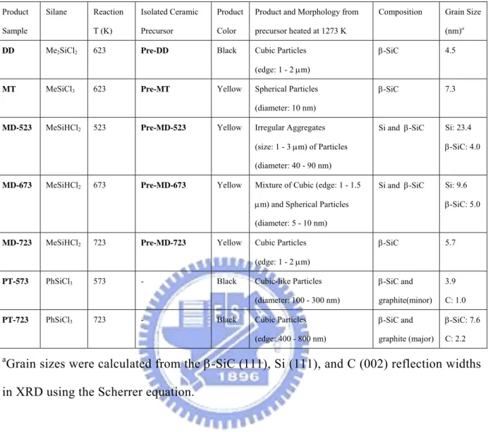
Table 2.1 Summary of reactions between sodium and organochlorosilanes. Product Sample Silane Reaction T (K) Isolated Ceramic Precursor Product Color
Product and Morphology from precursor heated at 1273 K
Composition Grain Size (nm)a
DD Me2SiCl2 623 Pre-DD Black Cubic Particles
(edge: 1 - 2 μm)
β-SiC 4.5
MT MeSiCl3 623 Pre-MT Yellow Spherical Particles
(diameter: 10 nm)
β-SiC 7.3
MD-523 MeSiHCl2 523 Pre-MD-523 Yellow Irregular Aggregates
(size: 1 - 3 μm) of Particles (diameter: 40 - 90 nm)
Si and β-SiC Si: 23.4 β-SiC: 4.0
MD-673 MeSiHCl2 673 Pre-MD-673 Yellow Mixture of Cubic (edge: 1 - 1.5
μm) and Spherical Particles (diameter: 5 - 10 nm)
Si and β-SiC Si: 9.6 β-SiC: 5.0
MD-723 MeSiHCl2 723 Pre-MD-723 Yellow Cubic Particles
(edge: 1 - 2 μm)
β-SiC 5.7
PT-573 PhSiCl3 573 - Black Cubic-like Particles
(diameter: 100 - 300 nm)
β-SiC and graphite(minor)
3.9 C: 1.0
PT-723 PhSiCl3 723 - Black Cubic Particles
(edge: 400 - 800 nm)
β-SiC and graphite (major)
β-SiC: 7.6 C: 2.2 aGrain sizes were calculated from the β-SiC (111), Si (111), and C (002) reflection widths
in XRD using the Scherrer equation.
2.3.1 Characterizations of Ceramic Precursors
SEM images of Pre-DD and Pre-MT are shown in Figures 2.1A and 2.1B as the examples for the morphology of the ceramic precursors. Pre-DD displays isolated cubic particles with edge lengths of 500 – 800 nm. Apparently, the particles contain a precursor shell layer which covers the surface of the inner cubic core. The image of Pre-MT shows a mixture of a precursor material and cubic particles with smooth surface. EDX data of the precursors (insets) suggest that they contain Na, Cl, Si, and C. A representative XRD pattern of Pre-DD, as shown in Figure 2.1C, can be indexed to NaCl.15 XRD data of the
Figure 2.1 SEM images of (A) Pre-DD, and (B) Pre-MT. (C) XRD pattern of Pre-DD. (Au
was sputtered to increase conductivity in EDX, and the peak marked with “*” is from the sample holder in XRD.)
FT-IR spectra of Pre-DD, Pre-MT, Pre-MD-673, and Pre-MD-723 are shown in Figure 2.2. The absorptions peaks are compared to literature values and listed in Table 2.2.10,16 The
most important feature is the peak near 800 cm-1, which can be assigned to Si-C stretching
1360 cm-1 while Si-H stretching is observed near 2100 cm-1. The information suggests that
polycarbosilane linkage containing Si-CH2-Si units is an important component in the ceramic
precursors. This also suggests that Kumada rearrangement is responsible for the structure formation.17 This is supported by the presence of absorptions from C-H vibrations. Signals
originated from moisture absorption in the samples are also observed.
Figure 2.2 FT-IR spectra of (A) Pre-DD, (B) Pre-MT,(C) Pre-MD-673, and (D)
Pre-MD-723. (The absorption bands marked with “*” are from absorbed H2O molecules,
and “#”is from atmospheric CO2 molecules.)
29Si solid state NMR spectra of Pre-DD, Pre-MT, Pre-MD-523, and Pre-MD-723 are shown
in Figure 2.3. The peaks are observed at -1.2, -17.1, -64.7, and -100.3 ppm. They are assigned to Si atoms in SiC4 (with four Si-C bonds), SiHC3 with one Si-H and three Si-C bonds),
results agreed with the FT-IR spectra data discussed above.
Table 2.2 FT-IR absorptions of the ceramic precursors.a
Vibration Mode Literatureb Pre-DD Pre-MT Pre-MD-673 Pre-MD-723
Si-C stretching 820 824 794 794 794 CH2 wagging of
Si-CH2-Si bond
1020 1012 1024 1042 1036
Si-Me deformation 1250 1254 1260 1278 1272 CH2 deformation
of Si-CH2-Si bond
1355 1369 1363 1351 1357
C-H deformation 1400 1454 1411 1405 1412 Si-H stretching 2100 2096 2114 2096 2084 C-H stretching 2900 2896 - - - C-H stretching 2950 2950 - - - a All absorption wavenumbers are in cm-1. b From refs 10 and 15.
Figure 2.3 29Si-SSNMR spectra of (A) Pre-DD, (B) Pre-MT, (C) Pre-MD-523, and (D)
2.3.2 SEM Characterizations
The ceramic precursors discussed above were heated at 1273 K to offer the final products DD, MT, MD-523, MD-673, MD-723, PT-573, and PT-723. Colors of the products were either black (DD, PT-573, and PT-723) or yellow (MT, MD-523, MD-673, and MD-723). We speculate that the concentration of free carbon affects the color of the products. FT-IR spectra of the samples in Figure 2.4 show a major absorption near 800 cm-1. This is assigned to the Si-C stretching of SiC.
Figure 2.4 FT-IR spectra of (A) DD, (B) MT, (C) MD-673, (D) MD-723, (E) PT-573, and (F) PT-723. (The Si-O peaks are silica from the quartz boat. The peak marked with “*” is from
absorbed H2O.)
SEM images of their morphology are shown in Figures 2.5A – 2.5F, respectively. In general, the products display cubic morphology except MT and MD-523. Each product will be briefly discussed below. As shown in Figure 2.5A, DD contains smooth surface cubes with edge lengths 1 - 2 μm. The powders of MT, displayed in Figure 2.5B, are spherical particles
Figure 2.5 High magnification SEM images of (A) DD, (B) MT, (C) MD-673, (D) MD-723,
(E) PT-573, and (F) PT-723. (Au was sputtered to increase conductivity in EDX.)
with diameters of ca. 10 nm. In Figure 2.5C, close examination of the image of MD-673 reveals that the cube surface is porous. In addition, some spherical particles can be found as a minor component in the corresponding low magnification SEM image in Figure 2.6C.
Figure 2.6 Low magnification SEM images of (A) DD, (B) MT, (C) MD-673 (In the red
circle, particle aggregates can be seen at high magnification), (D) MD-723, (E) PT-573, and (F) PT-723.
For MD-723, it shows a rough surface in Figure 2.5D. In Figure 2.5E, PT-573 appears to be aggregates of cubic shells with sizes of 100 – 300 nm. Collectively, these aggregates