超薄二氧化鉿閘極絕緣層之特性研究
73
0
0
全文
(2) 超薄二氧化鉿閘極絕緣層之特性研究 Characteristics of Ultra-Thin HfO2 Gate Insulator 學生:張宏迪 指導教授:張國明 博士. Student:Hong-Dyi Chang Advisor:Dr. Kow-Ming Chang. 國 立 交 通 大 學 電子工程學系. 電子研究所碩士班. 碩 士 論 文. A Thesis Submitted to Institute of Electronics College of Electrical Engineering and Computer Science National Chiao Tung University In Partial Fulfillment of the Requirements for the Degree of Master of Science In Electronics Engineering June 2005 Hsinchu, Taiwan, Republic of China. 中華民國 九十四 年 六 月.
(3) 超薄二氧化鉿閘極絕緣層之特性研究. 研究生:張宏迪. 指導教授:張國明 博士. 國立交通大學 電子工程學系 電子研究所碩士班. 摘. 要. 當場效電晶體的閘極介電層厚度微縮至 1.5 奈米厚時,將產生一些諸如電子 穿遂效應等嚴重的問題,因此極需以高介電係數材料取代二氧化矽作為閘極絕緣 層,其中二氧化鉿就是目前被認為最有可能取代二氧化矽的材料。本實驗以鋁二氧化鉿-矽之 MIS 電容結構為分析元件,首先利用直流濺鍍法沉積鉿金屬於 P 型和 N 型矽基板上,所沉積的金屬鉿厚度為 20 Å,接著以低溫通氧氣的爐管, 分別在 200℃、300℃、400℃和 500℃下以 15 分鐘或 30 分鐘氧化金屬鉿,得到 氧化鉿薄膜,其中部份試片在氧化後立刻以 850℃的快速熱退火處理 30 秒。在 不同氧化條件下的薄膜電性,經由 C-V 和 I-V 量測得知,並討論量子效應的漏電 流機制,另外也藉由磁滯效應、崩潰分佈、定電流加壓測試和在高溫下量測來討 論各種氧化條件下元件的可靠度。在相同的等效厚度下,二氧化鉿薄膜在 1 伏特 下的漏電流比二氧化矽薄膜少了兩個數量級以上。在相同的氧化條件下,P 型二 氧化鉿電容比 N 型二氧化鉿電容有較好的電特性及可靠度,氧化溫度越高會產生 越厚的介面層,使得薄膜等效厚度增加,可靠度也變差,但可改善磁滯效應。此 外,以快速熱退火處理二氧化鉿薄膜無法改善薄膜特性。. i.
(4) Characteristics of Ultra-Thin HfO2 Gate Insulator. Student:Hong-dyi Chang. Advisor:Kow-Ming Chang. Department of Electronics & Institute of Electronics National Chiao Tung University. ABSTRACT When the MOSFET gate insulator is scaled below 1.5 nm, some serious problems such as direct electric tunneling will occur. Therefore, high dielectric constant material is very desirable to replace SiO2. Hafnium oxide is a most promising material for future MOSFET gate oxide applications. In this study, we used Al-HfO2-Si MIS capacitor as our analysis device. First, we used DC sputter system to deposit 20 Å hafnium metal on p-type and n-type silicon substrate. Then we proceeded with furnace under 200 ℃ , 300 ℃ , 400 ℃ and 500 ℃ oxidation temperature and 15 or 30 minutes oxidation time to prepare HfO2 thin film. After oxidation process, we had an additional RTA treatment at 850℃ for 30 seconds. The electrical characteristics of the film under different oxidation condition were discussed by C-V and I-V curves. Moreover, the conduction mechanism with quantum effect was also analyzed. The reliability of the film under different oxidation condition was discussed by hysteresis effect, breakdown distribution, constant current stress and high temperature measurement. With the same equivalent oxide thickness (EOT), the magnitude of leakage current of HfO2 film is less than that of SiO2 film over 2 orders at 1 V. Under the same oxidation condition, p-type HfO2 capacitor has better electrical characteristics and reliability than n-type HfO2 capacitor. Under higher oxidation temperature, it would result in thicker interfacial layer, larger EOT, worse reliability but better hysteresis. In addition, RTA treatment couldn’t improve the quality of HfO2 film.. ii.
(5) 誌 謝 首先,我要感謝我的指導教授張國明老師,在這兩年中所給我指導與教誨, 使我在學術研究及待人處事上獲得長足的進步。 接著,我要感謝實驗室王敬業學長,在實驗過程中不斷的給予建議與指導, 並且提供我寶貴的經驗,以及其他實驗室的伙伴們,從旁陪伴以及協助,使得本 論文可以順利的完成。 另外,感謝國立交通大學半導體中心、國家奈米元件實驗室(NDL)提供我 良好的研究環境和設備,同時也要感謝技術人員熱心的協助,因此使我的研究可 以順利進行。而對於諸位口試委員的蒞臨指導與建議,在此也深表感謝之意。 最後,要感謝我的父母與親友,有了他們的支持與鼓勵,才能讓我在無後顧 之憂的情況下讓我順利完成學業與論文。. iii.
(6) Contents Abstract (in Chinese) ....................................................................................................i Abstract (in English) ....................................................................................................ii Acknowledgments (in Chinese)................................................................................... iii Contents .......................................................................................................................iv Table Captions ..............................................................................................................vi Figure Captions............................................................................................................vii. Chapter 1 Introduction 1.1 Background and Motivations........................................................................... 1 1.1.1 Scaling of Oxide Thickness .................................................................... 1 1.1.2 Roadmap of Gate Dielectric.................................................................... 2 1.2 High-k Material................................................................................................ 2 1.2.1 Advantages of High-k Material............................................................... 2 1.2.2 Challenges of High-k Material................................................................ 2 1.3 Why choose HfO2 ............................................................................................ 3 1.4 Thesis Organization ......................................................................................... 4 1.5 References........................................................................................................ 4. Chapter 2 Preparation methods of HfO2 2.1 ALCVD ............................................................................................................ 7 2.2 MOCVD........................................................................................................... 8 2.3 DC Magnetron Sputtering................................................................................ 9 2.4 References........................................................................................................ 9. Chapter 3 Experiments of Al/HfO2/Si MIS Capacitor 3.1 MIS Capacitors Fabrication Process..............................................................11 3.2 Sputtering system........................................................................................... 12 3.3 Furnace system............................................................................................... 12 3.4 Rapid Thermal Annealing system .................................................................. 13. Chapter 4 Electrical Characteristics of Al/HfO2/Si MIS Capacitors 4.1 Capacitance-Voltage Characteristics.............................................................. 14 4.2 Equivalent Oxide Thickness (EOT)............................................................... 15 4.3 Current-Voltage Characteristics ..................................................................... 16 iv.
(7) 4.3.1 Leakage Current.................................................................................... 16 4.3.2 Band-gap Diagram and Conduction Mechanism.................................. 19 4.4 RTA Treatment ............................................................................................... 21 4.5 References...................................................................................................... 22. Chapter 5 Reliability of Al/HfO2/Si MIS Capacitors 5.1 Hysteresis....................................................................................................... 24 5.2 Uniformity...................................................................................................... 24 5.3 Constant Current Stress (CCS) ...................................................................... 25 5.4 Measured at High Temperature...................................................................... 26 5.5 Reference ....................................................................................................... 26. Chapter 6 Conclusion and Future Work 6.1 Conclusion ..................................................................................................... 27 6.2 Future Work ................................................................................................... 28. v.
(8) Table Captions Chapter 1 Table 1-1. High-performance Logic Technology Requirements Roadmap. ( ITRS:2004 update ). Table 1-2. Reliability difficult challenges. ( ITRS:2004 update ). Table 1-3. Characteristics of various high-k materials.. Chapter 3 Table 3-1. The oxidation temperature and time of HfO2 films.. Chapter 4 Table 4-1. Measurement results of HfO2 capacitors with 6.25×10⁻⁶ cm2 die area.. Table 4-2. Measurement results of HfO2 capacitors with 2.5×10⁻⁵ cm2 die area.. Table 4-3. Measurement results of HfO2 capacitors with 1×10⁻⁴ cm2 die area.. vi.
(9) Figure Captions Chapter 1 Fig. 1-1. Conduction mechanism in oxide for the MOS structure.. Fig. 1-2. Gate leakage reduction by high-k dielectric. (B-Y Nguyen, 6th TRC October 27-28, 2003 Motorola). Fig. 1-3. LOP logic scaling-up of gate leakage current density limit and of simulated gate leakage due to direct tunneling. ( ITRS:2004 update ). Fig. 1-4. High-performance logic scaling-up of gate leakage current density limit and of simulated gate leakage due to direct tunneling. ( ITRS: 2004 update ). Fig. 1-5. Important high-k regions to be optimized for 1 nm high-k transistors. (International SEMATECH Confidential and Supplier Sensitive, 2002). Chapter 2 Fig. 2-1. ALCVD growth mechanism of AL2O3 and HfO2. (International SEMATECH Confidential and Supplier Sensitive, 2002). Fig. 2-2. Scaling limits of different ALCVD Hf-Based high-k Materials. (International SEMATECH Confidential and Supplier Sensitive, 2002). Fig. 2-3. Scaling limits of MOCVD HfO2 and ZrO2. (International SEMATECH Confidential and Supplier Sensitive, 2002). Chapter 3 Fig. 3-1. Fabrication flow chart of ultra thin HfO2 MIS capacitor.. Chapter 4 Fig. 4-1. 1MHz high frequency C-V characteristics of p-type HfO2 capacitors with different die areas under 400℃ 15 minutes oxidation condition.. Fig. 4-2. 1MHz high frequency C-V characteristics of p-type HfO2 capacitors with 6.25×10⁻⁶ cm2 die area under different oxidation conditions.. vii.
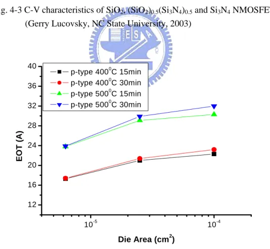
(10) Fig. 4-3. C-V characteristics of SiO2, (SiO2)0.5(Si3N4)0.5 and Si3N4 NMOSFET. (Gerry Lucovsky, NC State University, 2003). Fig. 4-4. EOT of p-type HfO2 capacitors with different die areas.. Fig. 4-5. EOT of p-type and n-type HfO2 capacitors with 6.25×10⁻⁶ cm2 die area under different oxidation conditions.. Fig. 4-6. Illustration of HfO2 capacitor.. Fig. 4-7. J-V characteristics of p-type HfO2 capacitors with different die areas under 400℃ 15 minutes oxidation condition from 0 V to -1 V.. Fig. 4-8. J-V characteristics of p-type HfO2 capacitors with 6.25×10⁻⁶ cm2 die area under different oxidation conditions from 0 V to -1 V.. Fig. 4-9. Measured and simulated J-V characteristics of NMOSFET with SiO2 gate insulator. The dotted line indicates the 1 A/cm2 limit for leakage current. (S. H. Lo, et. al (IBM), IEEE EDL 1997). Fig. 4-10. Gate leakage at ∣Vg∣= 1 V of n-type and p-type HfO2 capacitors with different die area.. Fig. 4-11. Gate leakage at ∣Vg∣= 1 V of n-type and p-type HfO2 capacitors with 6.25×10⁻⁶ cm2 die area under different oxidation condition.. Fig. 4-12. J-V characteristics of n-type and p-type HfO2 capacitors with 6.25×10⁻⁶ cm2 die area from -1 V to +1 V.. Fig. 4-13. Illumination of leakage current under negative bias. (a) energy band diagram (b) cross-section view. Fig. 4-14. J-V characteristics of n-type HfO2 capacitors with different die areas under 400℃ 15 minutes oxidation condition from 0 V to +10 V.. Fig. 4-15. J-V characteristics of p-type HfO2 capacitors with 6.25×10⁻⁶ cm2 die area under different oxidation conditions from 0 V to -10 V.. Fig. 4-16. Gate current as a function of the gate voltage for four oxide degradation stages in a 2000 µm2 SiO2 NMOSFET. After SBD, a large increase of the substrate current is observed in the whole voltage range. (Felice Crupi, et. al, IEEE Transactions on Electron Devices, 1998). Fig. 4-17. Four oxide degradation stages of p-type HfO2 capacitors with 6.25×10⁻⁶ cm2 die area under 400℃ 15 minutes oxidation condition.. Fig. 4-18. Energy band diagram of SiO2 capacitors with Al gate. viii.
(11) Fig. 4-19. Energy band diagram of HfO2 capacitors with Al gate.. Fig. 4-20. Conduction mechanism in the oxide for MIS structure.. Fig. 4-21. Schottky plot of n-type HfO2 capacitors with 6.25×10⁻⁶ cm2 die area under different oxidation condition.. Fig. 4-22. Fowler-Nordheim plot of n-type HfO2 capacitors with 6.25×10⁻⁶ cm2 die area under different oxidation condition.. Fig. 4-23. Frenkel-Poole plot of n-type HfO2 capacitors with 6.25×10⁻⁶ cm2 die area under different oxidation condition.. Fig. 4-24. 1MHz high frequency C-V characteristics of n-type HfO2 capacitors with 6.25×10⁻⁶ cm2 die areas under 400℃ 15 minutes oxidation condition without / with RTA.. Fig. 4-25. J-V characteristics of n-type HfO2 capacitors with 6.25×10⁻⁶ cm2 die areas under 400℃ 15 minutes oxidation condition without / with RTA.. Chapter 5 Fig. 5-1. Hysteresis of p-type HfO2 capacitors with 6.25×10⁻⁶ cm2 die area under different oxidation conditions. (a) 400℃ 15 minutes (b) 400℃ 30 minutes (c) 500℃ 15 minutes (d) 500℃ 30 minutes. Fig. 5-2. Hysteresis of n-type HfO2 capacitors with 6.25×10⁻⁶ cm2 die area under different oxidation conditions. (a) 300℃ 15 minutes (b) 400℃ 15 minutes (c) 400℃ 15 minutes (d) 500℃ 15 minutes. Fig. 5-3. Distribution of the breakdown voltage for p-type HfO2 capacitors with 6.25×10⁻⁶ cm2 die area under different oxidation conditions.. Fig. 5-4. Distribution of the breakdown voltage for n-type HfO2 capacitors with 6.25×10⁻⁶ cm2 die area under different oxidation conditions.. Fig. 5-5. Gate voltage shift of p-type HfO2 capacitors with 6.25×10⁻⁶ cm2 die area under different oxidation conditions as a function of stress time during Jg = 1 A/cm2 CCS stress.. Fig. 5-6. Gate voltage shift of n-type HfO2 capacitors with 6.25×10⁻⁶ cm2 die area under different oxidation conditions as a function of stress time during Jg = 1 A/cm2 CCS stress.. Fig. 5-7. C-V characteristics of n-type HfO2 capacitors with 6.25×10⁻⁶ cm2 die ix.
(12) area under 300℃ 15 minutes oxidation condition measured at 25℃, 75℃ and 125℃. Fig. 5-8. J-V characteristics of n-type HfO2 capacitors with 6.25×10⁻⁶ cm2 die area under 300℃ 15 minutes oxidation condition measured at 25℃, 75℃ and 125℃ from 0 V to 1 V.. Fig. 5-9. J-V characteristics of p-type HfO2 capacitors with 6.25×10⁻⁶ cm2 die area under 400℃ 15 minutes oxidation condition measured at 25℃, 75℃ and 125℃ from 0 V to -10 V.. x.
(13) Chapter 1 Introduction 1.1 Background and Motivations 1.1.1 Scaling of Oxide Thickness For more than 30 years, SiO2 films have been the preferred material for gate dielectric in metal-oxide semiconductor (MOS)-based structures. However, in order to increase the output of the products and reduce the cost, the scaling down of the device dimension is an inevitable tendency. In addition, the demand for the device performance and circuit stability is more and more strict, that means, high speed operation and low leakage current are necessary. To reach high speed, we can reduce channel length or lower operating voltage. If we lower operating voltage, we must raise the capacitance of gate oxide to maintain enough channel charges. Consequently, we need to reduce the oxide thickness to increase oxide capacitance. According to the SIA (Semiconductor Industry Association) roadmap, CMOS with gate length below 70 nm will need an oxide thickness of less than 1.5 nm, which corresponds to two or three layers of silicon dioxide atoms. But reducing the thickness of silicon dioxide to these dimensions results in an exponential increase of direct tunneling current [1]. The resulting gate leakage current will increase the power dissipation and will deteriorate the device performance and circuit stability for VLSI circuits. Figure 1-1 shows the several kinds of conduction mechanisms of the leakage current passing through the oxide layer, which contain hot carrier injection, Fowler-Nordheim tunneling and direct tunneling. When the oxide thickness is less than 2 nm, the dominant leakage mechanism is direct tunneling. This results that the leakage current increase rapidly with the decrease of the oxide thickness. From fig. 1-2, when the equivalent oxide thickness (EOT) is 2 nm, the leakage current density of SiO2 is 10-2 A/cm2, which is lower than logic limit but higher than wireless limit. We could use SiON to replace SiO2 and reduce the leakage current density about one order to make it lower than wireless limit. However, when the EOT is less than 2 nm, SiON also couldn’t be used for wireless application. In addition, the leakage of SiO2 even is larger than logic limit when the EOT is down to 1.5 nm, and SiON also couldn’t be used for logic application when the EOT is less than 1.3 nm. Thus, we have no choice but use high-k materials instead of SiO2 to be the gate insulator. High-k dielectrics could effectively reduce the leakage current density about 4 orders. 1.
(14) 1.1.2 Roadmap of Gate Dielectric Fig. 1-3 shows the low operating power (LOP) scaling-up of gate leakage current density limit and of simulated gate leakage due to direct tunneling. In 2005, the EOT is 1.4 nm and the leakage current density of the oxynitride is below the leakage limit line. However, after 2006, the EOT is below 1.3 nm and the oxynitride is incapable of meeting the limit on the gate leakage current density. Fig. 1-4 shows the high-performance logic scaling-up of gate leakage current density limit and simulated gate leakage due to direct tunneling. In 2006, the EOT is only 1 nm but the leakage current density of the oxynitride is still below the limit line because the application of high-performance logic could endure larger gate leakage current. However, after 2007, the oxynitride couldn’t be used for high-performance logic anymore. Table 1-1 is the roadmap of 2004 ITRS (International Technology Roadmap for Semiconductor) for the high-performance logic technology. After 2006, the requirement of EOT even reduces to less than 1 nm. It would be a big challenge because the leakage current is too large to be acceptable for SiO2 under such a thin thickness (Fig. 1-2). Replacing SiO2 by SiON could effectively reduce leakage current. However, fig. 1-4 shows that oxynitride is also incapable of meeting the limit on gate leakage current density. Therefore, we need to aggressively seek a feasible high-k material to replace SiO2.. 1.2 High-k Material 1.2.1 Advantages of High-k Material As SiO2 film is less than 2 nm, the leakage current becomes unacceptable. The direct way to reduce the leakage current is to make the oxide thickness thicker, which can repress the direct tunneling. According to the formula : C / A = εrε0 / tox , if we want the capacitance is still large enough, we need to choose some higher εr than that of SiO2 (εr = 3.9). The material with higher dielectric constant than 3.9 is called high-k material. Under the same EOT, we could expect that the leakage current of the high-k material is lower than that of the conventional SiO2 film due to the thicker physical thickness. In the last few years, high-k material has attracted a great deal of attention because of their potential for replacing SiO2 as gate dielectric in MOSFETs.. 1.2.2 Challenges of High-k Material Although high-k material is expected to replace SiO2 ideally, there are many problems to use high-k material practically. The issues for choosing a high-k material 2.
(15) may include: (1) low dielectric constant interfacial layer between substrate and high-k material (2) degradation of carrier mobility (3) shift of threshold voltage (4) thermal stability (5) boron penetration prevention (6) poly interface and poly gate electrode (7) compatibility with traditional CMOS process [1]-[4]. The high-k problems waiting to be solved is shown in fig. 1-5, which contains important regions consisting of the silicon interface and silicon interfacial layer, high-k film, and the interface between poly and high-k region (poly interfacial layer). The integration of the stack into a robust transistor flow is very crucial. The required high-k transistor integration is different than a baseline pure oxide or nitrogen-bearing gate dielectric. Unless special details are followed for the integration of the high-k material with the interfaces and subsequent transistor flow, the desired electrical properties will not be achieved. The specifications below are many electrical properties that will need to be achieved [5]: High Performance EOT ≦ 1 nm with leakage current density (Jg) ≦ 1.0 A/cm2 Low Standby Power ≦1.6 nm with Jg ≦ 2.2E-3 A/ cm2 Density of interface traps (Dit) ≦ 5E10 / cm2‧eV High frequency (100 kHz) capacitance-voltage (C-V) hysteresis ≦ 10 mV Thickness uniformity (3ρ) ≦ 4 % Thermal stability (physical and electrical) at 1000°C, 10 sec Surface mobility ≧ 95 % of SiO2 (current 2 nm baseline) High-k compatible post-gate etch clean strategy Reliability comparable to SiO2 (current 2 nm baseline) DRAM requirements for Jg (10-8 A/cm2) and thermal stability (1000°C, 60 sec) Table 1-2 shows the reliability challenges of high-k gate dielectrics, metal gate and copper/low-k interconnects. The main reliability issues include:(1) dielectric breakdown characteristics (hard and soft breakdown) (2) influence of charge trapping and NBTI on threshold voltage stability (3) stability and number of fixed charges. All the issues mentioned above still need more effort to overcome.. 1.3 Why choose HfO2 There are many kinds of high-k materials, including Al2O3, Y2O3, Ta2O5, TiO2, ZrO2 and HfO2 etc. Table 1-3 lists basic characteristics of several high-k dielectrics. Unfortunately, many high-k materials such as Ta205, TiO2, SrTiO3, and BaSrTi03 are thermally unstable when directly contacted with silicon [6] and need an additional barrier layer which may add process complexity and impose thickness scaling limit. 3.
(16) Also, materials with too low or too high dielectric constant may not be adequate choice for alternative gate dielectric application. Ultra high-k materials such as STO or BST may cause fringing field induced barrier lowering effect [7]. Materials with relatively low dielectric constant such as A12O3 and Y2O3 do not provide sufficient advantages over SiO2 or Si3N4 [8]. Among the medium-k materials compatible with silicon, oxides of Zr and Hf are attracting much attention recently. Especially, Hf forms the most stable oxide with the highest heat of formation (∆Hf = 27l Kcal/mol) among the elements in IVA group of the periodic table (i.e. Ti, Zr, Hf). Unlike other silicides, the silicide of Hf can be easily oxidized [9]. HfO2 possesses a dielectric constant of up to 25 [10], a large bandgap of 5.7 eV with sufficient band offset of larger than 1.5 eV [11], and well thermal stability in contact with silicon [12]. HfO2 is very resistive to impurity diffusion and intermixing at the interface because of it’s high density (9.68 g/cm3) [13]. In addition, HfO2 is the first high-k material showing compatibility with polysilicon gate process [14]. These properties make HfO2 one of the most promising candidates for alternative gate dielectric application. Although inadequate mobility of HfO2 MOSFETs is among the biggest concerns, various techniques have been explored to enhance the mobility. Introduction of strained silicon substrate [15], for example, drastically improved the mobility by changing the band structure of the substrate rather than changing the dielectric itself. However, the characteristics and mechanism of HfO2 are not totally understood.. 1.4 Thesis Organization Following chapters in the thesis are primarily organized as follow: In chapter 2, we make a comparison of various preparation methods of HfO2. In chapter 3, we make a description of experimental details. DC magnetron sputtering system is used to deposit hafnium on silicon surface. In chapter 4, we discuss the characteristics of ultra-thin HfO2 insulator by Metal-Insulator-Semiconductor (MIS) capacitors. In chapter 5, we discuss the reliability of ultra-thin HfO2 insulator by Metal-Insulator-Semiconductor (MIS) capacitors. In chapter 6, we make the conclusions for this thesis and provide some suggestions for future work.. 1.5 References 4.
(17) [1] Suehle, J. S.; Vogel, E. M.; Edelstein, M. D.; Richter, C. A.; Nguyen, N. V.; Levin, I.; Kaiser, D. L.; Wu, H.; Bernstein, J. B., “Challenges of high-k gate dielectrics for future MOS devices”, Plasma- and Process-Induced Damage, 2001 6th International Symposium on , 2001. [2] Salam, K. M. A.; Konishi, H.; Fukuda, H.; Nomura, S., “Reduction of leakage current of crystallized Ta2O5 through substitution with TiO2”, Gate Insulator, 2001. IWGI 2001. Extended Abstracts of International Workshop on, 2001 Page(s): 192 -195. [3] Jing-Chi Yu; Lai, B. C.; Lee, J. Y., “The fabrication and characterization of metal-oxide-semiconductor field effect transistors and gated diodes using Ta2O5 gate oxide”, Semiconducting and Insulating Materials Conference, 2000.SIMC-XI. International, 2000 Page(s): 353 -356. [4] Anri Nakajima, Quazi D. M. Khosru, Takashi Yoshimoto, Toshirou Kidera, and Shin Yokoyama, “NH3-annealed atomic-layer-deposited silicon nitride as a high-k gate dielectric with high reliability”, Appl. Phys. Lett. 80, 1252-1254 (2002). [5] International SEMATECH Confidential and Supplier Sensitive, “Status of High-k Gate Dielectric Development and the Demonstration of High-k Devices with Equivalent Oxide Thickness (EOT) of <= 1.0 nm”, 2002. [6] K. J. Hubbard and D. G. Schlom, J. Mater. Res. 11, 2757 (1996). [7] Baohong Cheng, Min Cao, Ramgopal Rao, Anand Inani, Paul Vande Voorde, Wayne M. Greene, Johannes M. C. Stork, Zhiping Yu, Peter M. Zeitzoff, Jason C. S. Woo, “The Impact of High-k Gate Dielectrics and Metal Gate Electrodes on Sub-100 nm MOSFET’s”, IEEE Transactions on Electron Devices, Vol. 46, No. 7, July 1999. [8] C. T. Liu, “Circuit Requirement and Integration Challenges of Thin Gate Dielectrics for Ultra Small MOSFET’s” in IEDM Tech. Dig., p.747, 1998. [9] S. P. Muraka and C. C. Chang, Appl. Phys. Lett. 37,639 (1980). [10] M. Balog, M. Schieber,M. Michman, and S. Patai, “Chemical vapor deposition and characterization of HfO2 films from organo-hafnium compounds,” Thin 5.
(18) Solid Films, vol. 41, pp. 247–259, 1977. [11] J. Robertson, “Band offsets of wide-band-gap oxides and implications for future electronic devices,” J. Vac. Sci. Technol. B, vol. 18, pp. 1785–1791, 2000. [12] K. J. Hubbard and D. G. Schlom, “Thermodynamic stability of binary oxides in contact with silicon,” J. Mat. Res., vol. 11, pp. 2757–2776, 1996. [13] M. Balog et al. Thin Solid Films, ~01.41, 247 (1977). [14] K. Onishi, C. S. Kang, R. Choi, H.-J. Cho, S. Gopalan, R. Nieh, S. Krishnan, and J. C. Lee, “Effects of high-temperature forming gas anneal on HfO2 MOSFET performance,” in VLSI Tech. Dig., 2002, pp. 22–23. [15] K. Rim, E. P. Gusev, C. D’Emic, T. Kanarsky, H. Chen, J. Chu, J. Ott, K. Chan, D. Boyd, V. Mazzeo, B. H. Lee, A. Mocuta, J. Welser, S. L. Cohen, M. Ieong, and H.-S. Wong, “Mobility enhancement in strained Si NMOSFETs with HfO2 gate dielectrics,” in VLSI Tech. Dig., 2002, pp. 12–13.. 6.
(19) Table 1-1 High-performance Logic Technology Requirements Roadmap. ( ITRS:2004 update ).
(20) Reliability Difficult Challenges Difficult Challenges High-k Gate Dielectrics. Summary of Issues 1. Dielectric breakdown characteristics (hard and soft breakdown) 2. Influence of charge trapping and NBTI on threshold voltage stability 3. Stability and number of fixed charges 1. Impact of metal-ion drift and/or diffusion on gate dielectric reliability 2. Work function control and stability. Metal Gate. 3. Metal susceptibility to oxidation 4. Thermo-mechanical issues due to large thermal expansion mismatch 5. Impact of implantation 1. Stress migration of Cu vias and lines 2. Cu via and line electromigration performance 3. Thermal-mechanical stability of the interfaces between metals, barriers. Copper / Low-k Interconnects. and interlevel dielectrics and resulting line-to-line leakage 4. Time Dependent Dielectric Breakdown (TDDB) of the Cu/low-k system 5. Reliability impact of lower thermal conductivity of low- k dielectric 6. Reliability issues due to the porous nature of the low- k dielectrics and moisture 7. Reliability impact of the lower mechanical strength in the Cu/low- k system, including the impact of packaging. Table 1-2 Reliability difficult challenges. ( ITRS:2004 update ).
(21) Material. Dielectric constant (k). Energy band gap Eg (eV). ΔEc (eV) to Si. ΔHF (eV/O atom). SiO2. 3.9. 8.9. 3.2. -4.68. Si3N4. 7. 5.1. 2. ─. Al2O3. 9. 8.7. 2.3. -5.76. Y2O3. 15. 5.6. 2.3. -4.93. CeO2. 26. 5.5. Ta2O5. 26. 4.5. 1-1.5. -2.09. La2O3. 30. 4. 2.3. -6.62. TiO2. 80. 3.5. 1.2. -4.86. HfO2. 25. 5.7. 1.5. -5.77. ZrO2. 25. 7.8. 1.4. -5.66. HfSixOy. 15-25. ~6. 1.5. -5.24. ZrSixOy. 12-25. 6.5. 1.5. -5.21. -5.02. Table 1-3 Characteristics of various high-k materials..
(22) Hot carrier injection. Fowler-Nordheim Tunneling. Direct Tunneling. Gate. Oxide. Substrate. Fig. 1-1 Conduction mechanism in oxide for the MOS structure.. SiON. SiO2 High-K. Fig. 1-2 Gate leakage reduction by high-k dielectric. (B-Y Nguyen, 6th TRC October 27-28, 2003 Motorola).
(23) Fig. 1-3 LOP logic scaling-up of gate leakage current density limit and of simulated gate leakage due to direct tunneling. ( ITRS:2004 update ). Fig. 1-4 High-performance logic scaling-up of gate leakage current density limit and of simulated gate leakage due to direct tunneling. ( ITRS:2004 update ).
(24) Fig. 1-5 Important high-k regions to be optimized for 1 nm high-k transistors. (International SEMATECH Confidential and Supplier Sensitive, 2002).
(25) Chapter 2 Preparation methods of HfO2 There are various methods to prepare high-k thin films, such as chemical vapor deposition (i.e. ALCVD, MOCVD, PECVD etc.) [1]-[3] and physical vapor deposition (i.e. Sputtering, PLD etc.) [4][5]. Among which, the usual methods for preparing HfO2 films are ALCVD, MOCVD and Sputtering. We compare these three methods below.. 2.1 ALCVD The major difference between conventional chemical vapor deposition (CVD) and ALCVD (atomic layer CVD) arises from how precursors are introduced to the substrate and how the substrate surface is applied to control growth. In ALCVD, precursors are introduced alternatively to the substrate surface with an inert gas purge between each. The precursors are not allowed to be in contact with each other in the gas phase. This results in a surface-controlled, layer-by-layer process for the deposition of thin films with atomic layer accuracy. Each atomic layer formed in the sequential process is a result of saturated surface controlled reactions. It provides well controlled growth of very thin films and excellent step coverage. Fig. 2-1 shows how ALCVD Al2O3 and HfO2 were deposited by ligand exchange reaction. Trimethyl aluminum Al(CH3)3 (TMA) and H2O were used for Al2O3 deposition and hafnium tetrachloride HfCl4 and H2O were used for HfO2 deposition. Much more detail on the surface chemistry is presented elsewhere [6]. ALCVD Hf-based high-k materials have demonstrated the feasibility of EOT scaling down to 1 nm by using HfAlxOy on nitrided surfaces [7]. HfO2 with Al2O3 in it, such as HfAlxOy or HfO2/Al2O3/HfO2, shows much better scaling capability than just HfO2. Fig. 2-2 shows the scaling limits of different Hf-based high-k materials for ALCVD. HfO2 could be utilized but was unable to scale below ~1.7 nm. HfSixOy deposition has shown great promise and has been scaled to 1.6 nm with leakage current four orders of magnitude lower than SiO2. The physical defects observed in the thin HfO2 limit the physical thickness scaling. However, the charge trapping is worsened by the presence of Al2O3. It has been found that the interfacial layers and high-k bulk materials both are very important for suppressing traps in high-k 7.
(26) dielectric. Some initial physical analysis data suggests the O3 chemical oxide may be a very promising approach for EOT scaling of ALCVD high-k stacks because chemical oxide has been demonstrated as a good starting surface for ALCVD growth. The rapid thermal SiO2 or SiON grown at the reduced partial pressure of reaction gases also is considered a possible solution for further reducing interfacial layer thickness. In the future, the project will focus on solving the charge trapping and mobility degradation of HfO2 with Al2O3 in it. Besides the electrical characterizations of ALCVD high-k materials, the issues related to manufacturing (such as uniformity, repeatability, and cost of ownership (COO)), need to be addressed before ALCVD high-k can be used in the IC industry. The uniformity and repeatability of HfO2 is quite reasonable (std. dev. 3–4%) [7]. But the COO is another big problem. Currently, ALCVD is a very slow process. The deposition time for a 3 nm HfO2 film is over 4 min without counting time for stabilization, pumping down and up, and wafer transfer. This can result in a total of 10–15 min for 2–4 nm HfO2 deposition. The very slow throughput might be the major showstopper to using ALCVD tools for mass production.. 2.2 MOCVD MOCVD (metal-organic CVD) is a widely used technology for depositing a variety of thin films, including metal oxide and metal silicate films, for high-k gate dielectric applications. The basic steps in MOCVD deposition method are as follows: 1. MO precursor in company with N2 process gas and O2 process gas are injected into the reactor. 2. The sources are mixed inside the reactor and transferred to the deposition process chamber. 3. At the deposition process chamber, high temperature results in the decomposition of sources and other gas-phase reactions, forming the film precursors that are useful for film growth and byproducts. 4. The film precursors transport to the growth surface. 5. The film precursors absorb on the growth surface. 6. The film precursors diffuse to the growth site. 7. At the surface, film atoms incorporate into the growing film through surface reaction. 8. The byproducts of the surface reactions desorb from the surface. 9. The byproducts transport to the main gas flow region away from the deposition area toward the reaction. Then the wafer exits. 8.
(27) From fig. 2-3, it is apparent that 1 nm EOT can be achieved with MOCVD metal oxide films when a metal electrode is used. However, most of the devices with MOCVD HfO2 and HfSixOy when a poly-Si gate is used have EOT greater than 2 nm. Unlike metal electrode, using poly-Si electrode requires the high-k gate stack to go through a 1000°C/10 sec S/D activation anneal step. This step not only results in chemical and structural changes in the high-k film, but also affects interfaces between the high-k film/substrate and the high-k/poly-Si electrode. All devices fabricated with MOCVD ZrO2 and ZrSiO films using poly-Si gate electrode were too leaky to give any meaningful C-V results. In general, using poly-Si gate electrode results in around 0.7 to 1 nm higher EOT for gate stacks fabricated with HfO2 and HfSixOy gate dielectric films. This additional interfacial oxide thickness is too large to be acceptable. In view of this, the MOCVD is not a good tool for high-k material deposition with poly-Si gate. However, the MOCVD has very good throughput and can process a 25-wafer lot in ~2 hours (roughly 4X better than ALCVD). Thus, from a throughput perspective, the MOCVD has a distinct advantage over the ALCVD [7].. 2.3 DC Magnetron Sputtering The usual HfO2 film with DC magnetron sputtering method is reactively sputtered from an Hf target in an Ar + O2 ambient onto Si substrate. The advantages of the DC magnetron sputtering are simple and cheap. In addition, the HfO2 film prepared by CVD system easily contains organic impurities and/or oxygen vacancies inside. This will cause leakage current through Frenkel-Pool effect or trap assisted tunneling [8]. Less contaminants are produced by the process of the sputtering because there is no other unnecessary chemicals. However, the uniformity of the DC sputtering is worse than that of the ALCVD and the MOCVD in 12 inch diameter Si wafer. Further, sputtering in an O2 ambient easily produces SiO2 interfacial layer. Therefore, we decide to sputter Hf in an Ar ambient only. After pure Hafnium has been deposited on Si substrate, we put the wafer into furnace system with O2 ambient at some low temperature for oxidation. At some low temperature (<500℃), Si will not react with O2 to form the SiO2. Then, the HfO2 film is prepared without SiO2 interfacial layer.. 2.4 References [1] R. J. Carter, E. Cartier, M. Caymax, S. De Gendt, R. Degraeve, G. Groeseneken, 9.
(28) M.Heyns, T. Kauerauf, A. Kerber, S. Kubicek, G. Lujan, L. Pantisano, W. Tsai, E. Young, “Electrical Characterisation of High-K Materials Prepared by Atomic Layer CVD”, IWGI 2001, Tokyo. [2] Benjamin Chih-ming Lai, Nan-hui Kung, and Joseph Ya-min Lee, “A study on the capacitance--voltage characteristics of metal-Ta2O5-silicon capacitors for very large scale integration metal-oxide-semiconductor gate oxide applications”, J. Appl. Phys. 85, 4087 1999. [3] Wai Shing Lau, Merinnage Tamara Chandima Perera, Premila Babu, Aik Keong Ow, Taejoon Han, Nathan P. Sandler, Chih Hang Tung, Tan Tsu Sheng and Paul K. Chu, “The Superiority of N2O Plasma Annealing over O2 Plasma Annealing for Amorphous Tantalum Pentoxide (Ta2O5) Films”, Jpn. J. Appl. Phys. Vol.37 pp.L435-L437 1998. [4] Y. Chuo, D. Y. Shu, L. S. Lee, W. Y. Hsieh, M. –J. Tsai, A. Wang, S. B. Hung, P. J. Tzeng, Y. W. Chou, “In-Line Inspection on Thickness of Sputtered HfO2 and Hf Metal Ultra-Thin Films by Spectroscopic Ellipsometry”, 2004 IEEE. [5] Takeshi Yamaguchi, Hideki Satake, Noburu Fukushima, “Band Diagram and Carrier Conduction Mechanisms in ZrO2 MIS Structures”, IEEE Transactions on Electron Devices, Vol. 51, No. 5 May 2004. [6]. Suvi Haukka, Marko Tuominen Europa/Semieducation, April 5th,2000.. and. Ernst. Granneman,. Semicon. [7] International SEMATECH Confidential and Supplier Sensitive, “Status of High-k Gate Dielectric Development and the Demonstration of High-k Devices with Equivalent Oxide Thickness (EOT) of <= 1.0 nm”, 2002. [8] Wai Shing Lau, Thiam Siew Tan, Nathan P. Sandler, Barry S. Page, “Characterization of Defect States Responsible for Leakage Current in Tantalum Pentoxide Films for Very-High-Density Dynamic Random Access Memory (DRAM) Applications”, Jpn. J. Appl. Phys., Vol.34, pp.757-761, 1995.. 10.
(29) Fig. 2-1 ALCVD growth mechanism of AL2O3 and HfO2. (International SEMATECH Confidential and Supplier Sensitive, 2002). Fig. 2-2 Scaling limits of different ALCVD Hf-Based high-k Materials. (International SEMATECH Confidential and Supplier Sensitive, 2002).
(30) (International SEMATECH Confidential and Supplier Sensitive, 2002). Fig. 2-3 Scaling limits of MOCVD HfO2 and ZrO2..
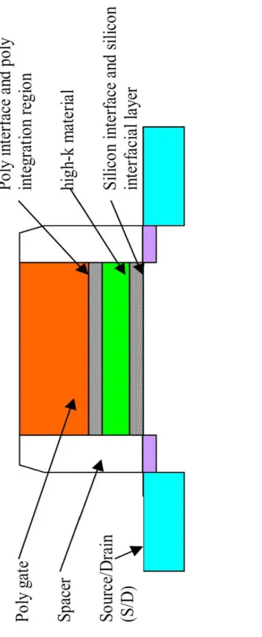
(31) Chapter 3 Experiments of Al/HfO2/Si MIS Capacitor 3.1 MIS Capacitors Fabrication Process In this thesis, isolated Al gated capacitors were fabricated to study ultra thin HfO2 gate dielectrics. Figure 3-1 shows the fabrication flow of this experiment. The starting wafer was four inch (100) orientated n-type wafer with phosphorus doped or p-type wafer with boron doped. It was one side polished and its resistivity was 5~10 ohm-cm. After standard initial RCA cleaning, wafers were put into furnace and grew a 5000Å thermal oxide layer at 1050℃. The oxide thickness was measured by a well-calibrated ellipsometer at a wavelength of 632.8 nm with the refractive index set at 1.462. Mask #1 defined the active regions and initial clean was performed again. Then, continued with DC magnetron sputtering hafnium on the wafers and oxidized them in furnace system. The thickness of as-deposit hafnium thin films was 20 Å which was read by the sensor inside the sputtering system. During sputtering, chamber pressure was maintained around 7.6×10⁻³ torr and the flow rate of Ar was 24 standard cubic centimeters per minute (sccm). The oxidation conditions were 200℃, 300℃, 400℃ and 500℃ respectively for 15 or 30 minutes, as shown in Table 3-1, with oxygen flow rate 5000 sccm. After oxidation process, pure aluminum was thermally evaporated on the top side of wafers. Mask #2 defined the top electrode. Then, we used wet etching to etch undefined Al and HfO2 films. After patterning, backside native oxide was stripped with diluted HF solution, and Al was deposited as bottom electrode. Finally, samples were sintered in pure N2 at 400℃ in furnace for 30min to recover the process induced damages. The detailed fabrication process flow was listed as follows. 1. Initial RCA cleaning. 2. Thermally grow 5000Å wet oxide at 1050℃. 3. Mask #1:define active region and then RCA clean again. 4. DC magnetron sputtering hafnium 20 Å. 11.
(32) 5. Thermal oxidize hafnium in furnace in an O2 ambient at 200℃, 300℃, 400℃ and 500℃ respectively for 15 or 30 minutes. 5-1. RTA treatment at 850℃ for 30 seconds. 6. Thermally evaporate 5000 Å aluminum as top electrode. 7. Mask #2:define top electrode and then wet etch undefined Al and HfO2 films. 8. Strip backside native oxide and coat 5000 Å aluminum as bottom electrode. 9. Al sintering in pure N2 at 400℃ in furnace for 30min. After the Al/HfO2/Si MIS capacitors were prepared, we used semiconductor parameter analyzer (HP4156A) and C-V measurement (HP4284) to analysis electric characteristics (i.e. I-V, C-V, EOT, leakage current density etc.). Then we tested their reliability, including stress induced leakage current (SILC), constant current stress (CCS), constant voltage stress (CVS), Hysteresis effect.. 3.2 Sputtering system Four inch high purity hafnium target was used to deposit thin film by DC magnetron sputtering system. The sputtering conditions were as follows. In the DC sputtering process chamber, the wafers were mounted on a face-down holder which can rotate during deposition to increase film uniformity. The system was pumped down to 2×10⁻⁶ torr first. This process made the chamber clean enough and thus decreased the impurity of the deposited hafnium film. Then the deposition pressure was controlled at 7.6×10⁻³ torr. Before started to deposit hafnium, the surface of the hafnium target was treated by low power pre-sputtering cleaning for ten minutes. The inert gas source was argon (Ar) and its flow rate was 24 sccm. It has heavy atomic weight and could be served as a heavy iron to knock down the hafnium atoms on the target surface. Therefore, the hafnium atoms could be sputtered onto the wafers. The thickness of the deposited hafnium was read by the sensor inside the sputtering system. Then, the oxidation process of hafnium was performed by furnace system. The DC magnetron sputtering power was set at 120 W and the corresponding deposition rate was 0.3 Å/s. The thickness of hafnium films was 20 Å.. 3.3 Furnace system 12.
(33) After hafnium had been deposited on silicon, we need an oxidation process to make it become hafnium dioxide. These Si wafers deposited with hafnium films were immediately loaded into furnace tube just as the sputtering process was finished. To start with, the tube temperature was set at 200℃, 300℃, 400℃ and 500℃ respectively as different process conditions and sufficient N2 gas was purging continuously. After the tube temperature was stable in five minutes letter, N2 gas was closed and O2 gas was introduced. The oxygen gas flow rate was set at 5000 (sccm). We provided sufficient oxygen gas and proper time to oxidize these films.. 3.4 Rapid Thermal Annealing system. METAL RTA-AG 610 was a single-wafer lamp-heated and computer-controlled rapid thermal processing (RTP) system. Water and compressed dry air (CDA) cooling system were used to cool down the quartz chamber. High intensity visible radiation heating and cold-heating chamber walls allow fast wafer heating and cooling rate. The 12 tungsten-halogen lamps were distinguished into five groups, and the relative percentage of lamp intensity can be adjusted individually for each group to achieve uniform temperature distribution. Temperature was obtained from pyrometer and precise controlled by computer. Two gas lines were used in the system which can be switched between Ar and N2. Before RTA process started, one minute N2 gas purge was performed to minimize the water vapor introduced during wafer loading and also swept unwanted particles induced during process. A fast heating rate of 60℃/s was chosen in this work. When anneal was complete, chamber temperature was quickly cooled down from 850℃ to 500℃ by N2 purge 30 seconds. Then, the chamber was slowly cooled down to 280℃ without N2 purge to avoid creaking of films. After five minutes later, wafers can be taken out from the chamber. By two-steps-cooling method, films’ creaks can be avoided. 13.
(34) Wafer Wafer Type Number. Oxidation Temperature (℃). Oxidation Time (minute). 200. 15. 2. 300. 15. 3. 200. 15. 300. 15. 1 p-type. n-type 4 5. 15 400. 6. 30 p-type. 7. 15 500. 8. 30. 9. 15 400. 10. 30 n-type. 11. 15 500. 12. 30. Table 3-1 The oxidation temperature and time of HfO2 films..
(35) 1. Initial RCA clean. 2. Thermally grow 5000 Å wet oxide. 3. Mask #1:define active region and RCA clean.. 4. Sputtering 20 Å hafnium. 5. Thermal oxidize hafnium films in furnace. (200℃, 300℃, 400℃ and 500℃ / 15 or 30 minutes) 5-1. RTA treatment at 850℃ for 30 seconds. 6. Thermal coating 5000 Å aluminum on top.. 7. Mask #2:pattern top electrode and etch Al and HfO2. 8. Strip native oxide on backside and coat bottom Al electrode. 9. Al sintering (N2_400℃_30min).. Figure 3-1 Fabrication flow chart of ultra thin HfO2 MIS capacitor..
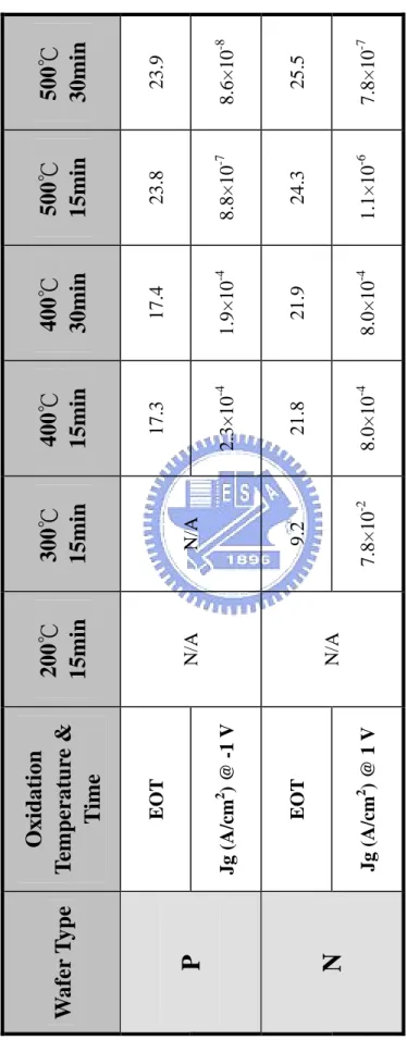
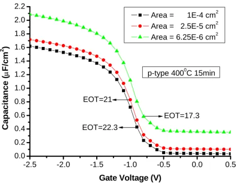
(36) Chapter 4 Electrical Characteristics of Al/HfO2/Si MIS Capacitors 4.1 Capacitance-Voltage Characteristics In our experiments, we used HP2484A LCR meter to measure the 1MHz high frequency C-V characteristics of our MIS capacitors. We swept the gate bias from inversion region to accumulation region. There were three different die areas (i.e. 6.25×10⁻⁶, 2.5×10⁻⁵ and 1×10⁻⁴ cm2) for discussing area depend effects. In addition, the oxidation temperature was ranging from 200℃ to 500℃ with 15 or 30 minutes. Table 4-1 shows the measurement results of HfO2 capacitors under different process conditions with 6.25×10⁻⁶ cm2 die area. Unfortunately, while the oxidation temperature is lower than 400℃, we only get the effective C-V characteristics of n-type HfO2 capacitors under 300℃ 15minutes oxidation condition. The failure in quasi-static C-V measurement is due to the leakage current higher than the displacement current for most gate bias. Under such a low oxidation temperature, hafnium atoms may react with oxygen atoms to form HfO2 but with very weak chemical bonding. We find that this weakly bonding type of HfO2 layer couldn’t bear much gate bias but it has an effective accumulation capacitance. It seems that n-type HfO2 capacitors could have stronger chemical bonding than p-type HfO2 capacitors under low oxidation temperature. Table 4-2 and 4-3 show the measurement results of HfO2 capacitors with 2.5×10⁻⁵ cm2 and 1×10⁻⁴ cm2 die area respectively. Fig. 4-1 shows the 1MHz high frequency C-V characteristics of p-type HfO2 capacitors with different die area under 400℃-15 minutes oxidation condition. We could see that the capacitors with smaller die area have larger accumulation capacitance, but the size of die area doesn’t influence the flat band voltage (VFB). Besides, the slopes of these three C-V curves are almost the same. Fig. 4-2 shows the 1MHz high frequency C-V characteristics of p-type HfO2 capacitors with 6.25×10⁻⁶ cm2 die area under different oxidation conditions. Under 400℃-15 minutes oxidation condition, the capacitor has the largest accumulation capacitance and the smallest ∣VFB∣. The higher oxidation temperature and the longer oxidation time make the more negative flat band voltage shift. There exists several types of charges, including 14.
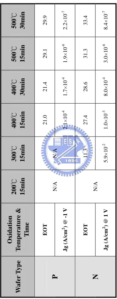
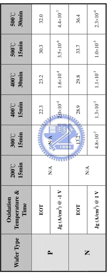
(37) interface trapped charge (Qit), fixed oxide charge (Qf), oxide trapped charge (Qot) and mobile ion (Qm), in the dielectric layer and at the substrate interface. To simplify, we call all these charges as interface effective positive charge Qi (C/cm2). So, the flat band voltage can be expressed as follows: V FB = Φ MS −. Qf C ox. −γ. Qm Q Q (Φ ) Q − γ ot − it S ≈ Φ MS − i C ox C ox C ox Ci. The influence of Qi is to introduce an equivalent negative charge within semiconductor. Because the work function difference and interface effective positive charge will both make the band near semiconductor surface bending downward, a negative voltage must be applied on metal to reach flat-band condition [1]. Thus, the more negative VFB means more positive charges were produced at the interface during oxidation process. Fig. 4-3 shows C-V characteristics of three different gate dielectrics, including SiO2, (SiO2)0.5(Si3N4)0.5 and Si3N4 [2]. ∆VFB for nitride and oxynitride devices with respect to oxide device are 0.15 and 0.04 V. Interfacial fixed charge is 7.5×10¹¹/cm2 for nitride and 2×10¹¹/cm2 for oxynitride. The fixed charge of the nitride film shows greater than oxynitride gate stack. This is due to increased bond-strain in the bulk and at internal dielectric interface. Increased bond-strain results in more “border traps”. Comparing fig. 4-2 to fig. 4-3, ∆VFB for HfO2 under 400℃-15 minutes oxidation condition with respect to SiO2 device is about 0.2 V. This is because of more stress in the HfO2 device, which generates more intrinsic defects, including bulk traps in film, border traps and interfacial traps. In addition, oxidation temperature affects ∆VFB seriously. The higher oxidation temperature would cause more stress in the device and generate more intrinsic defects. It may be caused by our improper cool down process. These defects directly influence the quality of the insulator layer and the substrate interface (i.e. gate leakage, carrier mobility, reliability etc.). In addition, 400℃ oxidation temperature makes the slope of C-V curve apparently stepper than 500℃ oxidation temperature. It seems oxidation time doesn’t affect the slope of C-V curve. Consequently, for p-type HfO2 capacitor, under 400℃-15 minutes oxidation condition could obtain the best C-V characteristics.. 4.2 Equivalent Oxide Thickness (EOT) From C-V characteristics, like fig. 4-1 and fig.4-2, equivalent oxide thickness (EOT) could be obtained by the following formula: tox = εr‧ε0‧A / C Where εr is the dielectric constant of SiO2 (εr = 3.9), ε0 is the permittivity in vacuum 15.
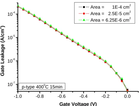
(38) (ε0 = 8.85×10⁻¹⁴ F/cm). A is the area of the capacitors (A = 6.25×10⁻⁶, 2.5×10⁻⁵ and 1×10⁻⁴ cm2) and C is the accumulation capacitance measured at ∣VG - Vt∣= 1 V at 1 MHz. According to this formula, we could calculate all the electrical EOT of our capacitors, which listed in Table 4-1, 4-2 and 4-3. We see that n-type HfO2 capacitors with 6.25×10⁻⁶ cm2 die area under 300℃-15 minutes oxidation condition have the smallest EOT of 9.2 Å. For p-type HfO2 capacitors, with 6.25×10⁻⁶ cm2 die area under 400℃-15 minutes oxidation condition have the smallest EOT of 17.3 Å. In addition, under the same oxidation condition, we find that p-type capacitors have smaller EOT than n-type capacitors. It might be attributed to that the diffusion rate of hafnium and oxygen atoms in n-type substrate is larger than in p-type substrate. Fig. 4-4 shows EOT of p-type HfO2 capacitors with different die areas. Under every different oxidation conditions, the devices with smaller die area have the smaller EOT. It is a very strange phenomenon. Devices with different die area on the same wafer under the same oxidation condition should have the same EOT. It is probably due to that the smaller die area attracts the larger ratio of edge charges around the device and thus has larger capacitance measured by HP4284, as shown in fig 4-1. If we eliminate the edge charge effect, the devices with different die area on the same wafer have the same EOT in fact. Fig. 4-5 shows EOT of p-type and n-type HfO2 capacitors with 6.25×10⁻⁶ cm2 die area under different oxidation conditions. Higher oxidation temperature causes larger EOT of the device. Besides, longer oxidation time also slightly increase EOT of the device. The increase of EOT might result from the increase of interfacial layer which grown in the oxidation process. As shown in fig 4-6, during oxidation process, hafnium and oxygen atoms would diffuse to substrate and form an HfSiO interfacial layer. We will discuss the possible reasons of such EOT tendency by analyzing current-voltage characteristics.. 4.3 Current-Voltage Characteristics 4.3.1 Leakage Current Fig. 4-7 shows the J-V characteristics of p-type HfO2 capacitors with different die areas (6.25×10⁻⁶, 2.5×10⁻⁵ and 1×10⁻⁴ cm2) under 400℃-15 minutes oxidation condition from 0 V to -1 V. We observed that the gate leakage current density becomes only a little larger while die area decreases. From table 4-1, 4-2 and 4-3, EOT of these three devices are 17.3 Å, 21.0 Å and 22.3 Å respectively. Fig. 4-8 shows J-V characteristics of p-type HfO2 capacitors with 6.25×10⁻⁶ cm2 die area under different oxidation conditions (400℃-15 minutes, 400℃-30 minutes, 500℃-15 16.
(39) minutes and 500℃-30 minutes) from 0 V to -1 V. The EOT of these four devices are 17.3 Å, 17.4 Å, 23.8 Å and 23.9 Å respectively. Apparently, the device under higher oxidation temperature and longer oxidation time has lower gate leakage current. In fig. 4-7, 5 Å increase of EOT (from 17.3 Å to 22.3 Å) only reduces a little gate leakage at VG = -1 V. But in fig. 4-8, 6.5 Å increase of EOT (from 17.3 to 23.8 Å) reduces gate leakage even more than 2 orders at VG = -1 V. Thus, from fig. 4-7, three similar magnitudes of gate leakage reveal that the thickness of devices with three different die area on the same wafer might be the same. As shown in fig. 4-8, the main reason of such a large repression of gate leakage between 400℃-15 minutes and 500℃-15 minutes oxidation conditions is the increase of thickness. Higher oxidation temperature could also make HfO2 film have stronger chemical bonding to effectively resist gate leakage. Besides, the devices under 500℃-15 minutes (EOT = 23.8) and 500℃-30 minutes (EOT = 23.9) oxidation condition have almost the same thickness but have about an order difference of gate leakage at VG = -1 V. Thus, the longer oxidation time mainly increases the intensity of chemical bonding. Fig. 4-9 shows measured and simulated J-V characteristics of NMOSFET with SiO2 gate insulator. Gate leakage current density of 20 Å SiO2 gate insulator at VG = 1 V is about 3×10⁻² A/cm2. From fig.4-9, however, gate leakage current density of the HfO2 capacitor with EOT = 17.3 Å at VG = -1 V is only about 3×10⁻⁴ A/cm2. Even thinner EOT of HfO2 capacitor but has less gate leakage than SiO2 device about 2 orders. Consequently, replacing SiO2 with HfO2 for gate insulator could effectively reduce gate leakage. Then, we make plots of gate leakage versus EOT for further discussing. As shown in fig. 4-10, we could obviously find that, whether for n-type or for p-type HfO2 capacitors, gate leakage at ∣Vg∣= 1 V of different die areas are almost the same, even if their EOT are not the same. With the increase of EOT, however, the gate leakage doesn’t decrease. Consequently, we think the EOT of devices with different die areas on the same wafer should be the same in fact. From fig. 4-11, we observe that, whether for n-type or for p-type HfO2 capacitors, while the oxidation temperature rises, the EOT becomes larger and the leakage becomes less. Higher oxidation temperature makes the HfSiO interfacial layer become thicker, as shown in fig. 4-6. The thicker interfacial layer causes the larger EOT of HfO2 gate insulator. Higher oxidation temperature also makes the chemical bonding stronger. Thicker physical thickness and stronger chemical bonding both contribute to the decrease of gate leakage current. Longer oxidation time slightly increases EOT and decreases gate leakage current. In addition, another interesting phenomenon is that under the same 17.
(40) oxidation condition, n-type HfO2 capacitor has larger EOT but larger gate leakage current than p-type HfO2 capacitor. The larger EOT might result from the larger diffusion rate of hafnium in company with oxygen atoms in n-type substrate than in p-type substrate. Generally, the device with larger EOT has less leakage current. Thus, we think the HfO2 layer grown on p-type substrate has better quality of resisting gate leakage than on n-type substrate. Fig.4-12 shows J-V characteristics of n-type and p-type HfO2 capacitors with 6.25×10⁻⁶ cm2 die area from -1 V to +1 V. For p-type, the leakage current under positive gate bias is much lower than negative case by 3 orders. For n-type, the leakage current under negative gate bias is lower than positive case by 1 order. The reverse leakage is thought to be dominated by surface leakage [3]. The surface generation current has been reported to be linearly correlated to the interface state density [4]. These interface states are caused by the dangling bonds at the Si/SiO2 interface [5][6]. This component is often masked by surface leakage, especially at low temperatures [7][8]. This is illustrated in fig. 4-13. Fig. 4-14 shows J-V characteristics of n-type HfO2 capacitors with different die areas under 400℃-30 minutes oxidation condition from 0 V to +10 V. In this figure, we could see the devices with 6.25×10⁻⁶, 2.5×10⁻⁵ and 1×10⁻⁴ cm2 die area, generate breakdown at VG = 3.85 V, 3.50 V and 3.10 V respectively. The device with smallest die area has the biggest breakdown voltage (VBD), which means the best quality of resisting leakage current. We think more ratio of leakage current could pass through the gate insulator from edge side between HfO2 layer and isolation oxide in the device with smaller die area. The leakage current which doesn’t pass through HfO2 layer doesn’t destroy the structure of HfO2 layer. Thus, the device with less ratio of leakage current passing through the HfO2 layer could have larger breakdown voltage. Fig.4-15 shows J-V characteristics of p-type HfO2 capacitors with 6.25×10⁻⁶ cm2 die area under different oxidation conditions (400℃-15 minutes, 400℃-30 minutes, 500℃-15 minutes and 500℃-30 minutes), correspond separating EOTs with 17.3 Å, 17.4 Å, 23.8 Å and 23.9 Å, from 0 V to -10 V. Breakdown voltages of these four devices are -6.05 V, -6.30 V, -7.15 V and -7.50 V. We could find that the device with thinner thickness and weaker chemical bonding generates breakdown more easily. In addition, like SiO2, thicker HfO2 shows more abrupt breakdown characteristics compared to thinner HfO2. Fig. 4-16 displays gate current as a function of the gate voltage for four oxide degradation stages in a 2000 µm2 SiO2 NMOSFET. After SBD, a large increase of the 18.
(41) substrate current is observed in the whole voltage range [9]. Fig. 4-17 shows four oxide degradation stages of p-type HfO2 capacitors with 6.25×10⁻⁶ cm2 die area under 400℃ 15 minutes oxidation condition. Like SiO2 NMOSFET, HfO2 capacitor has four degradation stages. This hints HfO2 might have similar breakdown mechanism with SiO2.. 4.3.2 Band-gap Diagram and Conduction Mechanism Selecting a gate dielectric with a higher permittivity than that of SiO2 is an essential choice. The required permittivity must also be balanced against barrier height to limit tunneling. For electrons traveling from the silicon substrate to the gate, this barrier is the conduction band offset, ∆EC. A gate dielectric must have a sufficient ∆EC value to poly-Si, and to other gate materials, in order to obtain low off-state currents (leakage). If the experimental ∆EC is < 1.0 eV, it will likely preclude the oxide's use in gate dielectric applications because thermal emission or tunneling would lead to unacceptably high leakage currents [10]. Among the several materials that have been investigated as gate dielectrics, as shown in Table 1-3, the dielectric constant generally exhibits an inverse relationship to the energy band gap. Fig. 4-18 shows the energy band diagram of the SiO2 MIS capacitor with Al gate. The energy band gap of SiO2 is 8.9 eV. Fig. 4-19 shows the energy band diagram of the HfO2 MIS capacitor with Al gate. The energy band gap of HfO2 is 5.7 eV [10]. The electron affinity 2.82 eV for HfO2 is obtained from the measurement of Fowler-Nordheim tunneling current of metal/ HfO2/Si MIS capacitors [11]. Taking the work function of Al as ФAl = 4.1 eV, the barrier height of Al/ HfO2 is ФAl/ HfO2 = 1.28 eV and the barrier height of HfO2/Si is ФSi/ HfO2 = 1.13 eV. There are many possible conduction mechanisms in insulators [12]. For SiO2, the dominate conduction mechanism was believed to be Fowler-Nordheim tunneling in the medium field (6~10MV/cm), low temperature region (T<200℃) [13]. As the thickness scales down, it would show the direct tunneling characteristics [14]. The weak temperature dependence of this tunneling process is well-known. The schematic illumination of conduction mechanism is shown in fig. 4-20, including Schottky emission, F-N tunneling, and Frenkel-Poole emission. The leakage current governed by the Schottky emission is as following: JSK = A* T2 exp{ -q[φB - ( qE / 4πεoεd )1/2 ] / kT }. 19.
(42) where A* is a constant, φB is the potential height on the surface, E is the electric field, ε0 is the permittivity in vacuum, εd is the dynamic dielectric constant, T is the temperature, and k is the Boltzmann constant. Fig. 4-21 shows the Schottky plot of n-type HfO2 capacitors with 6.25×10⁻⁶ cm2 die area under different oxidation conditions. The gray filled circles on each curve indicate where the individual slope of the curves becoming constant, which means the generation of Schottky emission happened. For the substrate electron injection case, the experimental results fit the Schottky emission theory well. While electric field is between 1 MV/cm to 16 MV/cm, the fitting slopes are almost constant. N-type HfO2 capacitors under 300℃-15 minutes oxidation condition begins to generate Schottky emission at VG = 0.09 V. Even for n-type capacitors under 500℃-30 minutes oxidation condition, which have largest EOT, Schottky emission occurs at very low bias VG = 0.82 V. Fowler-Nordheim (FN) tunneling is the flow of electrons through a triangular potential barrier illustrated in fig. 4-20. Tunneling is a quantum mechanical process similar to throwing a ball against a wall often results that the ball goes through the wall without damaging the wall or the ball. It also loses no energy during the tunnel event. The probability of this event happening, however, is extremely low, but an electron incident on a barrier typically several nm thick has a high probability of transmission. The FN current (IFN) is given by the expression [15]: ⎛−B⎞ ⎟⎟ I FN = AG Aε ox2 exp⎜⎜ ⎝ ε ox ⎠. where the AG is the gate area, ε ox is the oxide electric field, and A and B are usually considered to be constants. A and B are given as the following:. ⎞ q 3 ⎛⎜ m ⎟ m ox ⎠ = 1.54 × 10 −6 A= ⎝ 8πhΦ B B=. 8π 2mox Φ 3B 3qh. ⎞ ⎛m ⎜ m ⎟ A ⎤ ox ⎠ ⎡ ⎝ 2 ⎥ ⎢ Φ B ⎣V ⎦. ⎡V ⎤ m = 6.83 × 10 7 ⎛⎜ ox ⎞⎟Φ 3B ⎢ ⎥ m ⎠ ⎝ ⎣ cm ⎦. where mox is the effective electron mass in the oxide, m is the free electron mass, and Φ B is the barrier height at the silicon-oxide interface given in units of eV in the expression for B. Φ B is actually an effective barrier height that take into account barrier height lowering and quantization of electrons at the semiconductor surface. Rearranging I FN formula gives by: 20.
(43) ⎛ I ln⎜⎜ FN 2 ⎝ AG ε ox. ⎞ ⎛J ⎟ = ln⎜ FN ⎟ ⎜ ε2 ⎠ ⎝ ox. ⎞ B ⎟ = ln ( A) − ⎟ ε ox ⎠. A plot of ln(JFN/εox2) versus 1/εox should be a straight line if the conduction through the oxide is pure Fowler-Nordheim conduction [15]. The slop of linear F-N plot gives A and the intercept yields B. Fig. 4-22 shows F-N plot of n-type HfO2 capacitors with 6.25×10⁻⁶ cm2 die area under different oxidation conditions. The gray filled circles on each curve indicate the slopes of the each curves becoming constant, which means the generation of F-N tunneling happened. N-type HfO2 capacitors under 300℃-15 minutes oxidation condition begins to generate F-N tunneling at VG = 1.42 V. We could find that device with thinner EOT generates F-N tunneling at smaller gate bias. It is consistent with our prediction. The leakage current governed by Frenkel-Poole emission is as following: JFP = B‧E‧exp{ -q[φt - ( qE / πεoεd )1/2 ] / kT } where B is a constant, φt is the barrier height of trap level. The Frenkel-Poole emission is due to the field-enhanced thermal excitation of trapped electrons into the conduction band. Fig. 4-23 shows Frenkel-Poole plot of n-type HfO2 capacitors with 6.25×10⁻⁶ cm2 die area under different oxidation condition. The gray filled circles on each curve indicate the slopes of the curves becoming constant, which means the generation of Frenkel-Poole emission happened. N-type HfO2 capacitors under 300℃-15 minutes oxidation condition begins to generate Schottky emission at VG = 0.21 V. While electric field is between 4 MV/cm to 16 MV/cm, the fitting slopes are almost constant, indicating Frenkel-Poole emission is one conduction mechanism of leakage current. Even for n-type capacitors under 500℃-30 minutes oxidation condition, which have largest EOT, Schottky emission occurs at very low bias VG = 0.92 V. From above, we could find that Schottky emission occurs at very low gate bias and F-N tunneling occurs at higher gate bias than both Schottky emission and Frenkel-Poole emission. In addition, n-type HfO2 capacitors under 300℃-15 minutes oxidation condition always generate Schottky emission, F-N tunneling or Frenkel-Poole emission happened earliest because of smallest EOT.. 4.4 RTA Treatment In our experiments, after oxidation process, we could have an additional RTA treatment at 850℃ for 30 seconds to HfO2 film. Fig. 4-24 shows 1MHz high 21.
(44) frequency C-V characteristics of n-type HfO2 capacitors with 6.25×10⁻⁶ cm2 die areas under 400℃-15 minutes oxidation condition without / with RTA. The device with RTA treatment has smaller accumulation capacitance and smaller slope of C-V curve than without RTA treatment. Fig. 4-25 shows J-V characteristics of n-type HfO2 capacitors with 6.25×10⁻⁶ cm2 die areas under 400℃-15 minutes oxidation condition without / with RTA. The device with RTA treatment has larger leakage current than without RTA treatment. From above results, we know that RTA treatment couldn’t improve the quality of HfO2 film in J-V and C-V characteristics. This is due to HfO2 is unit-combined structure and thus couldn’t be enhanced the value of dielectric constant by RTA treatment. In the other hand, high-k material, like Ta2O5, which isn’t unit-combined structure could be enhanced the value of dielectric constant by RTA treatment [16]. In addition, when the temperature rises to 800℃~900℃, HfO2 would change the lattice structure from amorphous type to polycrystalline type and thus increase gate leakage current. Consequently, we don’t suggest using RTA treatment to HfO2 film.. 4.5 References [1] Ben G.. streetman, Sanjay Banerjee, “Solid State Electronic Devices”, 2001. [2] Gerry Lucovsky Departments of Physics, Electrical and Computer Engineering, and Materials Science and Engineering, NC State University, “Intrinsic limitations on the performance and reliability of high-k gate dielectrics: differences between interfacial and bulk bond-strain in high-k and SiO2 gate stacks.” [3] R. N. Hall, “Bulk generation current in depleted germanium junctions”, Appl. Phys. Lett. 29, 202 (1976). [4] Yea-Dean Sheu and Gilbert A. Hawkins, “Method for reduction in surface generation current in polycrystalline-silicon-gate metal-oxide-semiconductor devices”, J. Appl. Phys. 73, 4694 (1993). [5] E. Carnes and W. F. Kosonocky, RCA Rev. 33, 327 (1979). [6] P. J. Caplan and E. H. Poindexter, J. Appl. Phys. 50, 5847 (1979). [7] R. C. de Wit and J. M. McKenzle, IEEE Trans, Nuci. Sci. NS-16, 352 (1968). 22.
(45) [8] R. H. Pehl, E. E. Haller, and R. C. Cordt, IEEE Trans. Nuci. Sci, NS-20, 494 (1973). [9] Felice Crupi, Robin Degraeve, Guido Groeseneken, Senior Member, IEEE, Tanya Nigam, and Herman E. Maes, Fellow, IEEE, “On the Properties of the Gate and Substrate Current after Soft Breakdown in Ultrathin Oxide Layers”, IEEE Transactions on Electron Devices, Vol. 45, No. 11, November 1998 [10] J. Robertson, “Band Offsets of Wide-Band-Gap Oxides and Implications for Future Electronic Devices," J. Vac. Sci. Technol. B, Vol. 18, 2000, p. 1785. [11] W. Zhu, T.P. Ma, T. Tamagawa, Y. Di, J. Kim, R. Carruthers, M. Gibson, T. Furukawa, “HfO2 and HfAlO for CMOS : Thermal Stability and Current Transport”, in IEDM Tech. Dig., 20.4.1-4, 2001. [12] S. M. Sze, “Physics of Semiconductor Devices”, New York, Wiley, p.406, 1981. [13] S. S. Gong et al., “Evolution of Qbd for electrons tunneling from the Si/SiO2 interface compared to electron tunneling from the poly Si/SiO2 interface”, IEEE Transactions on Electron Devices, vol. 40, p.1251, 1993. [14] K. F. Schuegraf et al., “Reliability od Thin SiO2 at direct tunneling voltages”, in IEDM Tech. Dig., p.609, 1994. [15] Dieter K. Schroder, “Semiconder Material and Device Characterization” Wiley-INTERSCIENCE, 1998. [16] Hung-Yu Chen, “Characteristics of Ultra-thin Ta2O5 Gate Insulator”, 2003.. 23.
(46) N. P. Wafer Type. N/A. N/A. 200℃ 15min. 7.8×10⁻². 9.2. N/A. 300℃ 15min. 8.0×10⁻⁴. 21.8. 8.0×10⁻⁴. 21.9. 1.9×10⁻⁴. 17.4. 17.3 2.3×10⁻⁴. 400℃ 30min. 400℃ 15min. 1.1×10⁻⁶. 24.3. 8.8×10⁻⁷. 23.8. 500℃ 15min. Table 4-1 Measurement results of HfO2 capacitors with 6.25×10⁻⁶ cm2 die area.. Jg (A/cm2) @ 1 V. EOT. Jg (A/cm2) @ -1 V. EOT. Oxidation Temperature & Time. 7.8×10⁻⁷. 25.5. 8.6×10⁻⁸. 23.9. 500℃ 30min.
(47) N. P. Wafer Type. N/A. N/A. 200℃ 15min. 5.9×10⁻². 11.3. N/A. 300℃ 15min. 1.0×10⁻³. 27.4. 8.0×10⁻⁴. 28.6. 1.7×10⁻⁴. 21.4. 21.0 2.1×10⁻⁴. 400℃ 30min. 400℃ 15min. 29.1. 500℃ 15min. 3.0×10⁻⁶. 31.3. 1.9×10⁻⁶. Table 4-2 Measurement results of HfO2 capacitors with 2.5×10⁻⁵ cm2 die area.. Jg (A/cm2) @ 1 V. EOT. Jg (A/cm2) @ -1 V. EOT. Oxidation Temperature & Time. 8.4×10⁻⁷. 33.4. 2.2×10⁻⁷. 29.9. 500℃ 30min.
(48) N. P. Wafer Type. N/A. N/A. 200℃ 15min. 4.8×10⁻². 13.2. N/A. 300℃ 15min. 1.3×10⁻³. 28.9. 1.1×10⁻³. 29.8. 1.6×10⁻⁴. 23.2. 22.3 2.0×10⁻⁴. 400℃ 30min. 400℃ 15min. Table 4-3 Measurement results of HfO2 capacitors with 1×10⁻⁴ cm2 die area.. Jg (A/cm2) @ 1 V. EOT. Jg (A/cm2) @ -1 V. EOT. Oxidation Temperature & Time. 1.0×10⁻⁵. 33.7. 3.5×10⁻⁶. 30.3. 500℃ 15min. 2.3×10⁻⁶. 36.4. 4.4×10⁻⁷. 32.0. 500℃ 30min.
(49) 2.2. 2. Area = 1E-4 cm 2 Area = 2.5E-5 cm 2 Area = 6.25E-6 cm. 2.0 1.8 2. Capacitance (µF/cm ). 1.6 1.4 0. p-type 400 C 15min. 1.2 1.0 EOT=21. 0.8 0.6. EOT=17.3 EOT=22.3. 0.4 0.2 0.0 -2.5. -2.0. -1.5. -1.0. -0.5. 0.0. 0.5. Gate Voltage (V). Fig. 4-1 1MHz high frequency C-V characteristics of p-type HfO2 capacitors with different die areas under 400℃ 15 minutes oxidation condition.. 0. p-type 400 C 15min 0 p-type 400 C 30min 0 p-type 500 C 15min 0 p-type 500 C 30min. 2.2 2.0. 2. Capacitance (µF/cm ). 1.8 1.6 EOT=23.8. 1.4. EOT=17.3. EOT=17.4. 1.2 1.0 0.8. EOT=23.9. 0.6 0.4 0.2 0.0 -3.5. 2. Area = 6.25E-6 cm. -3.0. -2.5. -2.0. -1.5. -1.0. -0.5. 0.0. 0.5. Gate Voltage (V). Fig. 4-2 1MHz high frequency C-V characteristics of p-type HfO2 capacitors with 6.25×10⁻⁶ cm2 die area under different oxidation conditions..
(50) Fig. 4-3 C-V characteristics of SiO2, (SiO2)0.5(Si3N4)0.5 and Si3N4 NMOSFET. (Gerry Lucovsky, NC State University, 2003). 40 36 32. p-type p-type p-type p-type. 0. 400 C 0 400 C 0 500 C 0 500 C. 15min 30min 15min 30min. EOT (A). 28 24 20 16 12 10. -5. 10. -4. 2. Die Area (cm ). Fig. 4-4 EOT of p-type HfO2 capacitors with different die areas..
(51) 26. Area = 6.25E-6 cm. 2. 24 22. EOT (A). 20 18 16 14. p-type p-type n-type n-type. 12 10. oxidation oxidation oxidation oxidation. 15 30 15 30. min min min min. 8 300. 400. 500 0. Oxidation Temperature ( C). Fig. 4-5 EOT of p-type and n-type HfO2 capacitors with 6.25×10⁻⁶ cm2 die area under different oxidation conditions.. SiO2. Al HfO2 HfSiO. Si-substrate. Fig. 4-6 Illustration of HfO2 capacitor.. SiO2.
(52) 10. -4. 10. -5. 10. -6. 10. -7. 2. Gate Leakage (A/cm ). 2. Area = 1E-4 cm 2 Area = 2.5E-5 cm 2 Area = 6.25E-6 cm. 0. p-type 400 C 15min -1.0. -0.8. -0.6. -0.4. -0.2. 0.0. Gate Voltage (V). 10. -3. 10. -4. 10. -5. 10. -6. 2. Gate Leakage (A/cm ). Fig. 4-7 J-V characteristics of p-type HfO2 capacitors with different die areas under 400℃ 15 minutes oxidation condition from 0 V to -1 V.. 0. p-type 400 C 15min 0 p-type 400 C 30min 0 p-type 500 C 15min 0 p-type 500 C 30min. EOT=17.3 EOT=17.4. Area = 6.25E-6 cm. 2. EOT=23.8. 10. -7. 10. -8. 10. -9. -1.0. EOT=23.9. -0.8. -0.6. -0.4. -0.2. 0.0. Gate Voltage (V). Fig. 4-8 J-V characteristics of p-type HfO2 capacitors with 6.25×10⁻⁶ cm2 die area under different oxidation conditions from 0 V to -1 V..
數據


+7
相關文件
External evidence, as discussed above, presents us with two main candidates for translatorship (or authorship 5 ) of the Ekottarik gama: Zhu Fonian, and Sa ghadeva. 6 In
Although the standpoint of The Techniques of Samatha and Vipaśyana in Mah yāna Buddhism is different from the viewpoint of Hui-shih, its stress on the vajra prajñā is considered
如圖,已知平行四邊形 EFGH 是平行四邊形 ABCD 的縮放圖形,則:... 阿美的房間長 3.2 公尺,寬
For example, Liu, Zhang and Wang [5] extended a class of merit functions proposed in [6] to the SCCP, Kong, Tuncel and Xiu [7] studied the extension of the implicit Lagrangian
[r]
Without using ruler, tearing/cutting of paper or drawing any line, use the square paper provided (Appendix A) to fold the figure with the same conditions as figure 8b, but the area
mass/ strength 6-12 months 2-5 years Body fat redistribution 3-6 months 2-5 years Cessation of menses 2-6 months n/a. Clitoral enlargement 3-6 months 1-2 years Vaginal atrophy
effective price of choice in training: (wishfully) growth function m H (N) with a break point Lecture 6: Theory of Generalization. Restriction of
