152 IEEE JOURNAL OF SOLID-STATE CIRCUITS, VOL. 36, NO. 1, JANUARY 2001
A Reverse-Voltage Protection Circuit for MOSFET Power Switches
Hao-Ping Hong and Jiin-Chuan Wu, Member, IEEE
Abstract—When MOSFET is used as a power switch, it is
es-sential to prevent reverse current flow through the parasitic body diodes under reverse voltage condition. A new built-in reverse voltage protection circuit for MOSFETs has been developed. In this design, an area-efficient circuit is used to automatically select the proper well bias voltage to prevent reverse current under the reverse-voltage condition. This built-in reverse protection circuit has been successfully implemented in a high-side power switch application using a 0.6- m CMOS process. The die area of the protection circuit is only 2.63% of that of a MOSFET. The latch-up immunity is greater than+12 V and 10 V in voltage triggering mode, and greater than 500 mA in current triggering mode. The protection circuit is not in series with the MOSFET switch, so that the full output swing and high power efficiency are achieved.
Index Terms—CMOS, latch-up, power switch.
I. INTRODUCTION
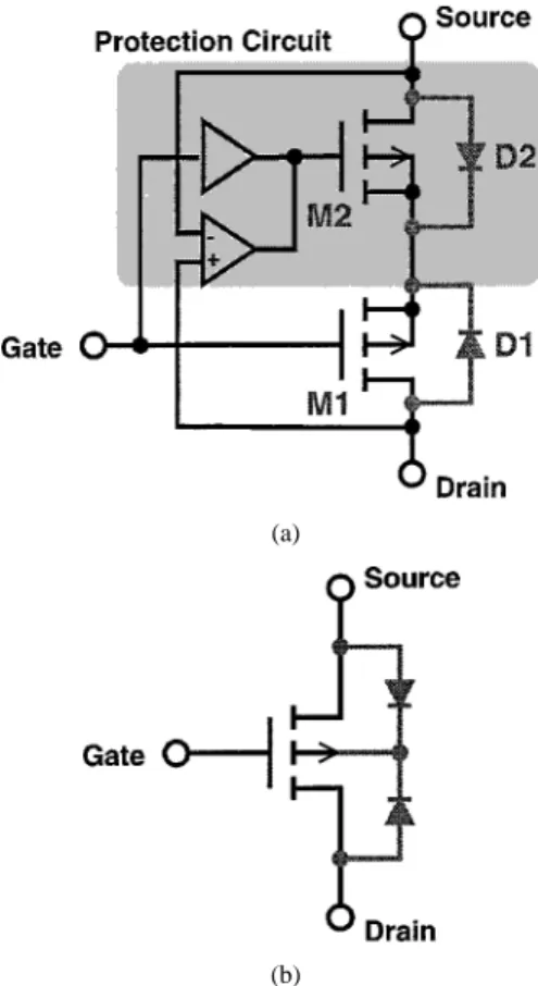
I
N THE firewire bus interfaces (e.g., USB, IEEE 1394, PCMCIA, and Card Bus), intelligent MOSFET protection switches [1]–[4] are desired to protect the power buses not only from bursts, surges, and short circuits during plug or unplug, but also from reverse current. This is to say, when the peripheral device has a higher supply voltage, the MOSFET switch must be able to isolate the power buses. In a MOSFET, there are inherent parasitic diodes formed by the drain–well and source–well junctions. Under the reverse voltage condition, the parasitic diodes will be turned on if the well or the substrate is not properly biased. Excessive current flow may destroy devices. To eliminate the reverse current problem, reverse battery protection (RBP) structure [5] and floating-well circuits [6]–[10] were proposed. The RBP structure, shown in Fig. 1(a), consumes large die area because a huge MOSFET M2 is needed to reduce voltage drop. The floating-well protection circuits [see Fig. 1(b)] are more cost-effective and power-efficient. However, the floating well is more susceptible to noise coupling which may cause latch-up due to increased junction leakage current. To improve latch-up immunity, a deep implant process and large guard-ring spacing were used [6], [7].In this paper, an area-efficient circuit is proposed to resolve these problems. This circuit automatically selects the proper n-well biasing voltage to prevent reverse current. The area of the protection circuit is only 2.63% of that of the MOSFET switch. The protection circuit is not in series with the MOSFET switch, so that the output swing and power efficiency are not affected. It
Manuscript received March 29, 2000; revised September 9, 2000. This re-search was supported by the National Science Council under Grant NSC89-2215-E-009-065 and by the Chip Implementation Center, Taiwan, R.O.C.
The authors are with the Department of Electronics Engineering, National Chiao-Tung University, Hsin-Chu, Taiwan 30050, R.O.C. (e-mail: jcwu@alab. ee.nctu.edu.tw).
Publisher Item Identifier S 0018-9200(01)00446-2.
(a)
(b)
Fig. 1. Circuit structures for reverse voltage protection.
also has robust electrostatic discharge (ESD) and latch-up per-formance. The proposed protection circuit is incorporated in an intelligent power switch IC, which is fabricated using a 0.6- m standard digital CMOS process.
II. BUILT-INREVERSE-VOLTAGEPROTECTIONCIRCUIT
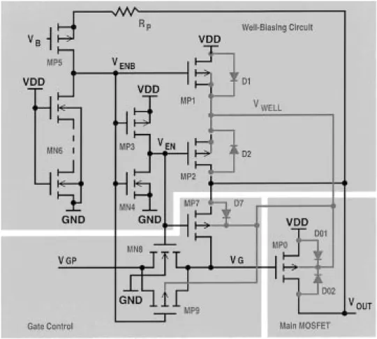
The circuit diagram of the built-in reverse-voltage protection (BRVP) method is shown in Fig. 2. It improves the disadvan-tages of floating-well method and RBP method. As mentioned previously, the floating-well method is more area-efficient than RBP method. However, it is susceptible to latch-up problems and cannot isolate the two power sources. The problem could be resolved by dynamically biasing the well to the higher voltage one between the drain terminal and source terminal. The prin-ciple of the dynamical well-biasing circuit in Fig. 2 is sim-ilar to that of the RBP method, except that the additional large MOSFET in the supply path is moved to the well pick-up path. Therefore, the sizes of MOSFET MP1 and MP2 for well biasing are small because the current needed for biasing the well is very small. Hence, the total area of MOSFET with BRVP method is almost the same as that of the floating-well method. Thus, it is cost-effective and latch-up free. Under reverse-voltage con-ditions, the well and gate of the MOSFET are connected to the
IEEE JOURNAL OF SOLID-STATE CIRCUITS, VOL. 36, NO. 1, JANUARY 2001 153
Fig. 2. Proposed BRVP circuit.
drain, so that the MOSFET and parasitic diodes are turned off to isolate the two power sources. The details of circuit operations with BRVP method are described below.
Referring to Fig. 2, as long as , the tran-sistor MP5 is turned off, where and are the threshold and gate voltages of MP5, respectively. Thus, and . Therefore, MP1 is turned on and MP2 is turned off. The well voltage, , of the main MOSFET MP0 is equal to . The transmission gate (MN8 and MP9) in the main MOSFET MP0’s gate-drive path is turned on, i.e., MP0 is directly driven by the gate-drive signal, . If is not con-nected to another voltage source, then is always smaller than . Therefore, for the MOSFET switch to function cor-rectly, it is required that . Under these con-ditions, transistor MP5 is always turned off, and the MOSFET MP0 behaves like a conventional MOSFET. Note that there is no dc current in the well-biasing circuit under these conditions. If a voltage source is connected at the output node so that , then MP5 is turned on. Note that, in this case, is greater than , because
. A very small ratio is used for MN6 so that once MP5 is turned on, the following is true: and . With these two voltage levels, MP1 is turned off and MP2 is turned on. The well voltage is connected to by MP2. Since is greater than , the para-sitic diodes D01 and D1 are reverse biased and no reverse cur-rent will flow through these diodes. In the meantime, MN8 and MP9 are turned off and MP7 is turned on. The gate voltage
of MP0, , is equal to , which ensures the MOSFET MP0 is turned off independent of the voltage . Thus, when , this circuit can prevent the reverse current by turning off the main MOSFET and keeping all the body diodes reverse biased. This circuit works well even if the power is turned off, i.e., or is floating.
The choice of the value of is important. To bias the well correctly and keep all the parasitic diodes turned off, there is
another constraint: , where
is the forward bias voltage of parasitic diode. Note that for in the range of , the well voltage
is still connected to . In this case, if , then for in the range of
, the diode D02 will be turned on. Therefore, the value of should be bounded by
. Typically, is larger than , i.e., should be smaller than . For example, let V, V, and V, then ideally should be in the range of 4.2 to 4.8 V. Generally, creating a voltage that is slightly less than the supply voltage is not too difficult. However, it requires additional circuits and dc currents. To avoid these penalties, is directly connected to in this design. In this case, when
, a reverse current will flow from through parasitic diodes D02 and D2 to , then through MP1 to . To minimize this reverse current, a small ratio should be used for MP1. Since the diodes D02 and D2 are forward biased, the reverse current will flow in the n-well and into the substrate. To prevent latch-up, proper
154 IEEE JOURNAL OF SOLID-STATE CIRCUITS, VOL. 36, NO. 1, JANUARY 2001
guard rings are required for these transistors. Note that these guard rings are needed even if a proper value is used for .
For example, let V, V, V, and
V, then for in the range of 5 to 5.3 V, is 5 V, i.e., the diodes D02 and D2 are slightly forward biased. Thus, guard rings are still needed to prevent latch-up.
For the ESD concern, when is directly connected to , the ESD protection poly resistor shown in Fig. 2 is needed to protect MP5. For the main MOSFET switch MP0, because it is used in hot-plug applications, the concerns about latch-up and ESD/electrical overstress (EOS) must be taken carefully. They are stated as followed. First, because MP0 is formed within an isolated n-well, it inherently has a better latch-up current blocking capability. However, as mentioned previously, double guard rings, inserted between MP0 and other nMOS circuits to block the latch-up current path, are still needed for latch-up pre-vention. Second, because the well of MP0 is automatically con-nected to the higher voltage between and , the ESD behavior of MP0 is like a reverse-biased diode, when a posi-tive or negaposi-tive voltage is stressed at pad with connected to ground. Because the minimum snapback holding voltage of pMOS is almost the same as the breakdown voltage, the phe-nomenon of snapback does not tend to occur. The ESD current of MP0 is discharged through the reverse junction breakdown. No ballast resistance is required. In the nMOS power switch case, the snapback characteristic is apparent. Inserting a ballast resistance to make ESD current discharged uniformly is nec-essary for nMOS to avoid ESD failures. With a ballast resis-tance, the drain-contact-to-gate spacing rule must be followed carefully in circuit layout. Under the constraint of this rule, to achieve the same ESD zapping level, nMOS requires much more area. Besides, if the substrate is grounded, the parasitic vertical bipolar p-n-p device (pad to n-well to p-substrate for diffusion well process only) also helps to bypass the ESD current, when an ESD voltage is stressed. Hence, using pMOS as a switch has more advantages in terms of ESD concerns. Third, the break-down voltage of pMOS is higher when compared with nMOS. In a 0.6- m process, the breakdown voltage of pMOS is about 13 V; however, the breakdown of nMOS is only about 11 V. For burst and surge current concerns of hot-plug interfaces, pMOS could meet the requirement of robust EOS reliability due to its higher breakdown voltage.
III. EXPERIMENTALRESULTS
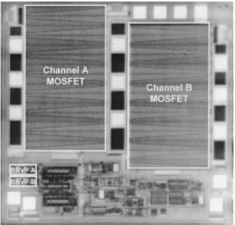
Based on the proposed reverse-current prevention design, a MOSFET with the BRVP circuit has been successfully imple-mented in a dual-channel intelligent high-side power switch using a 0.6- m CMOS logic process. Fig. 3 is the micropho-tograph of this power switch, where the main MOSFETs and reverse-voltage protection circuits are marked. It can be seen that the areas of BRVP circuits are small. The chip area in-cluding pads is 2547 m 2453 m. The size of the MOSFET is 180 mm/0.8 m. Its on-resistance is 70 m . Its die area is 920 m 1623 m. The die area of a BRVP circuit is 333 m
118 m, which is only 2.63% of a MOSFET.
Fig. 4 shows the reverse-current measurement results with V, , and opened, when a reverse voltage is
Fig. 3. Microphotograph of a dual-channel MOSFET power switch.
Fig. 4. Reverse current versus reverse voltage(I versusV )
applied to . The three curves show that the reverse cur-rents are small. When V, a peak reverse current of 1.119 mA occurs at V. As discussed in the pre-vious section, with , when
, transistor MP1 will not be turned off. Reverse current will flow from through D2 and D02, and Mp1 to . When exceeds 4.1 V, MP1 is turned off; the re-verse current reduces to 1 A. When , because
MN6 is OFF, , if . Hence, the
measured leakage is larger when V, with a peak current of 4 nA. When is floating, as is increased from 0 V, is slowly charged by the reverse current so that its voltage also rises. Thus it takes a larger (1.2 V) to turn on MP5, when compared with the -grounded case. The peak reverse current is 0.8 A. No latch-up occurs for all these static tests. Dynamic latch-up tests were performed according to JEDEC 17 standard, with fixed at 5 V. For the voltage triggering mode, up to 12 and 10 V, in 1 V steps, with re-spect to were performed without latch-up. For the current triggering mode, up to 500 mA, in 25 mA steps, were per-formed without latch-up. For the ESD protection, a filed-oxide
IEEE JOURNAL OF SOLID-STATE CIRCUITS, VOL. 36, NO. 1, JANUARY 2001 155
device (FOD) has been added for providing a ground discharge path. Based on the MIL-STD-883C 3015.7 Human Body Model (HBM) testing standard, the pin passes 8 kV ESD test in all four modes zapping.
Compared with the RBP circuits shown in Fig. 1(a), the pro-posed BRVP circuit has the advantages of full output voltage swing and smaller die area, due to the removal of the series-con-nected pMOS M2. Although the floating-well circuit shown in Fig. 1(b) does not have series-connected pMOS, its MOSFETs die area is larger than that of the BRVP for the same turn-on re-sistance. The reason is that a large distance (55 m) is needed between the source–drain junctions and the well edges to im-prove latch-up immunity [6]. It also needs an additional deep implant to construct a more effective guard ring for latch-up pre-vention. On the other hand, the proposed BRVP circuit is fabri-cated using standard digital CMOS process and standard layout design rules.
IV. CONCLUSION
A BRVP circuit for MOSFET used as power switch was pro-posed. A MOSFET with this BRVP circuit was incorporated in an intelligent power switch IC with diagnostics. It was imple-mented in a 0.6- m CMOS logic process. The well of the pMOS is automatically connected to its source or drain depending on which voltage is higher. Thus, the parasitic source–drain junc-tion diodes are always reverse-biased to prevent reverse cur-rent and latch-up. Under reverse-voltage conditions, the gate of MOSFET is connected to to isolate and . This protection circuit does not require any external control signals, thus it is also applicable for conventional three-terminal MOS-FETs. By moving the protection devices in the supply path into the well-biasing circuit, small devices can be used so that this circuit occupies very small areas. In our test chip, its area is only 2.63% of that of a MOSFET switch. The area penalty is small. With only one main MOSFET in the supply path, the
reverse-voltage protection circuit has the same advantages of full output voltage swings and higher power efficiency than a floating-well circuit does. However, by always connecting the n-well to the higher voltage between source and drain voltages, this circuit has better latch-up robustness than floating-well cir-cuits. Besides, a special deep-implant process is needed for the floating-well circuits. The measured results show the reverse-voltage protection circuit works well, even if the supply reverse-voltage is zero or is floating. The ESD protection is 8 kV. The latch-up immunity is greater than 12 and 10 V in voltage triggering mode, and greater than 500 mA in current triggering mode.
REFERENCES
[1] M. I. C. Simas, P. Santos, P. Casimiro, and M. Lanca, “Smart power in MOS technologies–An overview,” in ISIE ’97, Proc. IEEE Int. Symp.
Industrial Electronics, vol. 2, July 1997, pp. 371–376.
[2] B. J. Baliga, “An overview of smart power technology,” IEEE Trans.
Electron Devices, vol. 38, pp. 1568–1575, July 1991.
[3] R. Gariboldi and F. Pulvirenti, “A 70–m intelligent high-side switch with full diagnostics,” IEEE J. Solid-State Circuits, vol. 31, pp. 915–923, July 1990.
[4] E. Bruun, “Reverse-voltage protection method for CMOS circuits,”
IEEE J. Solid-State Circuits, vol. 24, pp. 100–103, Feb. 1989.
[5] K. Sakamoto, N. Fuchigami, K. Takagawa, and K. S. Ohtaka, “An in-telligent power MOSFET with reverse battery protection for automotive application,” in ISPSD Proc., May 1996, pp. 57–60.
[6] M. P. Vidal, M. Bafleur, J. Buxo, and G. Sarrabayrouse, “Latch-up test structures for reliability analysis of a floating-well-based smart power technology,” in ICMTS ‘93, Proc. Int. Conf. Microelectronic Test
Struc-tures, Mar. 1993, pp. 111–115.
[7] M. Bafleur, J. Buxo, M. P. Vidal, P. Givelin, V. Macary, and G. Sarrabay-rouse, “Application of a floating-well concept to a latch-up-free low-cost smart power high-side switch technology,” IEEE Trans. Electron
De-vices, vol. 40, pp. 1340–1342, July 1993.
[8] M. Ueda, A. Carl, J. Iadanza, H. Oshikawa, M. Yamamoto, M. Nelson, K. Key, Y. Tokuda, T. Saitoh, R. Kilmoyer, F. Jaquish, and M. Nishihara, “A 3.3-V ASIC for mixed voltage applications with shutdown mode,” in IEEE Custom Integrated Circuits Conf., May 1993, pp. 25.5.1–4. [9] M. J. M. Pelgrom and E. Carel Dijkmans, “A 3/5 V compatible I/O
buffer,” IEEE J. Solid-State Circuits, vol. 30, pp. 823–825, July 1995. [10] H.-C. Chow, “Bidirectional buffer for mixed voltage applications,” in
ISCAS ’99, Proc. 1999 IEEE Int. Symp. Circuits and Systems, vol. 1,