Transient-Induced Latchup in CMOS ICs
Under Electrical Fast-Transient Test
Cheng-Cheng Yen, Student Member, IEEE, Ming-Dou Ker, Fellow, IEEE, and Tung-Yang Chen, Member, IEEE
Abstract—The occurrence of transient-induced latchup (TLU) in CMOS integrated circuits (ICs) under electrical fast-transient (EFT) tests is studied. The test chip with the parasitic silicon-controlled-rectifier (SCR) structure fabricated by a 0.18-μm CMOS process was used in EFT tests. For physical mechanism characterization, the specific “swept-back” current caused by the minority carriers stored within the parasitic PNPN structure of CMOS ICs is the major cause of TLU under EFT tests. Different types of board-level noise filter networks are evaluated to find their effectiveness for improving the immunity of CMOS ICs against TLU under EFT tests. By choosing the proper components in each noise filter network, the TLU immunity of CMOS ICs against EFT tests can be greatly improved.
Index Terms—Board-level noise filter, electrical fast transient (EFT), latchup, silicon-controlled rectifier (SCR), transient-induced latchup (TLU).
I. INTRODUCTION
T
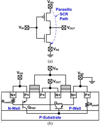
RANSIENT-INDUCED latchup (TLU) has been a pri-mary reliability issue in CMOS integrated-circuit (IC) products [1]–[5]. This TLU tendency is caused by several factors. First, aggressive scaling of device feature size, as well as the reduced clearance between PMOS and NMOS transis-tors, leads the inevitable parasitic silicon-controlled rectifier (SCR) in CMOS ICs to exhibit poor latchup immunity. The typical circuit structure and the device cross-sectional view of a CMOS inverter in digital ICs are shown in Fig. 1(a) and (b), respectively. The SCR structure in the inverter is formed by the parasitic PNPN (P+/N-well/P-well/N+) structure between the VDD and VSS of CMOS circuits. The equivalent circuitof the SCR structure is formed by a vertical PNP bipolar junction transistor (BJT) (QPNP) coupled with a lateral NPN
BJT (QNPN). When one of the BJTs is turned on, the
mech-anism of positive feedback regeneration in the SCR structure will be initiated [6]. If the product of beta gains of these two BJTs can be kept greater than one, the SCR structure will hold in a stable latching state. When the parasitic SCR in Manuscript received August 7, 2008; revised November 18, 2008 and December 30, 2008. First published March 10, 2009; current version published June 5, 2009. This work was supported in part by the National Science Council (NSC), Taiwan, under Contract NSC 97-2221-E-009-170 and in part by Himax Technologies Inc., Taiwan.
C.-C. Yen is with the Nanoelectronics and Gigascale Systems Laboratory, Institute of Electronics, National Chiao Tung University, Hsinchu 300, Taiwan. M.-D. Ker is with the Nanoelectronics and Gigascale Systems Laboratory, Institute of Electronics, National Chiao Tung University, Hsinchu 300, Taiwan, and also with the Department of Electronic Engineering, I-Shou University, Kaohsiung 84001, Taiwan (e-mail: [email protected]).
T.-Y. Chen is with the Basic Technology Department, Research and Devel-opment Center, Himax Technologies, Inc., Tainan 744, Taiwan.
Color versions of one or more of the figures in this paper are available online at http://ieeexplore.ieee.org.
Digital Object Identifier 10.1109/TDMR.2009.2015938
Fig. 1. (a) Circuit structure and (b) device cross-sectional view of a CMOS inverter.
CMOS ICs is triggered to cause latchup, it generates a low-impedance path from VDD to VSS with a high current that
often burns out the chip. It has also been reported that the latchup triggering current does not significantly increase with the scaling rule of CMOS processes while the power supply voltage keeps decreasing [7]. Second, there are much more complicated implementations of CMOS ICs, such as mixed signal, multiple power supplies, radio frequency (RF), system-on-chip, etc. The environment where these CMOS devices are located will suffer from considerable electrical transient disturbances coming from the exterior of CMOS ICs. Thus, such electrical transients, which are unpredictably coupled to the power, ground, or input/output (I/O) pins of CMOS ICs, will induce TLU much more often than before. Third, more and more ICs are rather susceptible to TLU under the strict require-ments of reliability test standards, such as the electrical fast-transient (EFT) test standard of IEC 61000-4-4 [8]. The I/O, data, and control ports of electronic products must sustain the EFT peak voltage of ±2 kV to achieve the immunity require-ment of “level 4” in the IEC 61000-4-4 test standard. It has been 1530-4388/$25.00 © 2009 IEEE
reported [9]–[12] that some CMOS ICs and microelectronic products are very susceptible to electrical transients, even though they have passed the component-level ESD specifica-tions such as human-body model (HBM) [13] of±2 kV, ma-chine model (MM) [14] of±200 V, and charged-device model (CDM) [15] of±1 kV.
It has been clarified that the “swept-back current” [16] caused by the electrical transients on the power (ground) pins of CMOS ICs is the major cause of TLU. TLU can be initiated by the swept-back current when an electrical transient on VDD
increases from its negative peak voltage to a positive voltage. Such a swept-back current is strongly dependent on the pa-rameters of the electrical transient voltage waveform, such as transient peak voltage, damping frequency, and duration time [17]. In real situations, however, all these parameters depend on the set voltage of EFT generator, metal traces of board-level (chip-board-level) layout, board-board-level noise filter network, etc. To suppress the occurrence of TLU, a board-level noise filter could be a solution to enhance the TLU immunity of CMOS ICs because the board-level noise filter network between the noise sources and CMOS ICs can decouple, bypass, or absorb noise voltage (energy) [18], [19]. Thus, the TLU immunity of CMOS ICs strongly depends on the board-level noise filter network. However, how the board-level noise filter network can enhance the TLU immunity of CMOS ICs against EFT tests has not been investigated so far.
In this paper, TLU induced in CMOS ICs by EFT tests is clearly studied [20]. Another purpose of this paper is to investigate a high-efficiency board-level noise filter network for TLU prevention under EFT tests. Different types of noise filter networks are evaluated to find their improvements to TLU immunity, including capacitor filter, ferrite bead, transient voltage suppressor (TVS), and several high-order noise filters such as L-section (second-order) and π-section (third-order)
RC filters. All the experimental results have been verified with
the SCR test structure fabricated in a 0.18-μm CMOS process.
II. EFT TEST
The IEC 61000-4-4 standard [8] defines immunity require-ments and test methods for electronic equipment against repet-itive fast transients. The repetrepet-itive EFT test is a test with bursts consisting of a number of fast pulses, coupled into the power supply, control, signal, and ground ports of electronic equipment. The characteristics of EFT tests are high amplitude, short rise time, high repetition rate, and low energy of the tran-sients. The EFT test is intended to demonstrate the immunity of electronic equipment to transient disturbances such as those originating from switching transients (interruption of inductive loads, relay contact bounce, etc.).
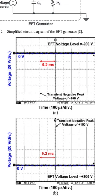
According to the IEC 61000-4-4 standard, the simplified circuit diagram of the EFT generator is shown in Fig. 2. In particular, only the impedance-matching resistor Rm (50 Ω) and the dc-blocking capacitor Cd(10 nF) are fixed. The charg-ing capacitor Ccis used to store the charging energy, and Rcis the charging resistor. The resistor Rsis used to shape the pulse duration. The effective output impedance of the EFT generator is 50 Ω [21].
Fig. 2. Simplified circuit diagram of the EFT generator [8].
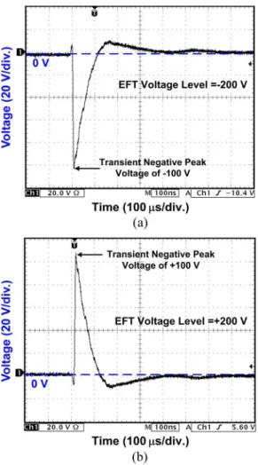
Fig. 3. Measured voltage waveforms on 50-Ω load under EFT tests with repetition rate of 5 kHz and EFT voltages of (a)−200 V and (b) +200 V.
The IEC 61000-4-4 standard defines the test voltage wave-forms of these fast transients with repetition frequencies of 5 and 100 kHz. The use of a 5-kHz repetition rate is the traditional EFT test, and 100 kHz is closer to reality. For an EFT pulse with a repetition frequency of 5 kHz, there are 75 pulses in each burst, and the burst duration time is 15 ms. For an EFT pulse with a repetition frequency of 100 kHz, there are 75 pulses in each burst, and the burst duration time is 0.75 ms. For both repetition rates, the burst repeats every 300 ms.
For EFT pulses with a repetition frequency of 5 kHz, the measured−200- and +200-V voltage waveforms on the 50-Ω load are shown in Fig. 3(a) and (b), respectively. Due to the im-pedance matching, the measured pulse peak is half of the input EFT pulse voltage. As shown in Fig. 3(a) and (b), the measured output pulse peaks on the 50-Ω load are−100 and +100 V, respectively. For the EFT repetition frequency of 5 kHz, the
Fig. 4. Measured voltage waveforms of a single pulse on 50-Ω load under EFT tests with EFT voltages of (a)−200 V and (b) +200 V.
time interval between each pulse is 0.2 ms. Under EFT tests, the application time should not be less than 1 min, and both polarities have to be tested. The minimum start values of the pulse peak are±200 V from the EFT tester. With the 50-Ω load, the voltage waveforms of a single pulse with EFT voltages of
−200 and +200 V are shown in Fig. 4(a) and (b), respectively.
In Fig. 4(a) and (b), the waveform of a single pulse has a rise time of about 5 ns and a pulse duration (time interval at half of the peak EFT voltage) of 50 ns.
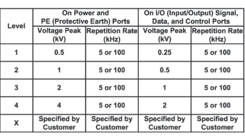
The EFT test levels for the power supply ports and the I/O, data, and control ports of equipment are listed in Table I. The voltage peak for testing I/O, data, and control ports is half of the voltage peak for testing power supply ports. The repetition rate is determined by specific products or product types. Level “X” is an open level that can be defined by the user. Level “X” is specified in the dedicated equipment specification. The output EFT voltage peak values are listed in Table II. With an output load of 1000 Ω, the measured output voltage peak equals to the open-circuit voltage peak multiplied by 1000/1050 (the ratio of the 1000-Ω test load to the total circuit impedance of 1000 plus 50 Ω). With an output load of 50 Ω, the measured output voltage is half of the value with an open-circuit load due to impedance matching.
Fig. 5(a) and (b) shows the emission microscope (EMMI) photographs of EFT-induced TLU failure in a 0.5-μm CMOS
IC product with a power supply voltage of 5 V. Fig. 5(a) shows the hot spots of latchup locations in the test chip after the EFT test, and Fig. 5(b) shows the corresponding zoomed-in latchup location, which is located across the boundary between NMOS and PMOS transistors in a digital logic block. From the test results shown in Fig. 5(a) and (b), under EFT tests, the parasitic SCR structure located across the boundary between NMOS and PMOS transistors can be initiated to cause latchup event. Due to the mechanism of positive feedback regeneration, the SCR structure can provide a low-impedance path to conduct high current from VDDto the ground to burn out the IC. This result
has demonstrated that the EFT test can trigger on the parasitic SCR structure to cause TLU event in real IC products. In this paper, an SCR structure is designed to clarify the TLU event and to investigate the mechanism under EFT tests with positive and or negative EFT voltages.
III. TESTSTRUCTURE
A. SCR Structure
The SCR structure is used as the test structure for TLU mea-surements under EFT tests because the occurrence of latchup is due to the inherent SCR in bulk CMOS ICs. The device cross-sectional view and layout top view of the SCR structure are shown in Fig. 6(a) and (b), respectively. The anode of the SCR is connected to the N+ and P+ diffusions in N-well, whereas the cathode of the SCR is connected to the N+ and P+ diffusions in P-well. The geometrical parameters such as SA,
SC, and SACrepresent the distances between the P+ diffusions in N-well, P+ and N+ diffusions in P-well, and P+ diffusion in N-well and N+ diffusion in P-well, respectively. In the SCR structure, the N+ and P+ diffusions in N-well are connected to VDD, whereas the N+ and P+ diffusions in P-well are
connected to the ground. Once latchup occurs through the SCR structure, a huge current will be generated by the mechanism of positive-feedback regeneration [6]. As a result, the huge current will conduct through the low-impedance path from VDD
to the ground and further probably burn out the chip due to ex-cess heat.
In this paper, to investigate the occurrence of TLU under EFT tests, the SCR structure with the layout parameters of
SA= 29.12 μm, SC = 14.25 μm, and SAC= 4 μm in a
0.18-μm CMOS process with 3.3-V devices is used for TLU measurements.
B. Turn-On Mechanism
The equivalent circuit schematic of the SCR structure is shown in Fig. 7(a). The SCR structure consists of a lateral NPN BJT (QNPN) and a vertical PNP BJT (QPNP) to form a
two-terminal/four-layer PNPN (P+/N-well/P-well/N+) structure. The switching voltage of the SCR device is dominated by the avalanche breakdown voltage of the N-well/P-well junction, which could be as high as∼19 V in a 0.18-μm CMOS process. When the positive voltage applied to the anode of the SCR is greater than the breakdown voltage of the N-well/P-well junction, with its cathode being relatively grounded, hole and
TABLE I EFT TESTLEVELS
TABLE II
OUTPUTVOLTAGEPEAK(VP) VALUES ANDREPETITIONRATES
electron currents will be generated through the avalanche break-down mechanism. The hole current will flow through the P-well to the grounded P+ diffusion, whereas the electron current will flow through the N-well to the N+ diffusion connected to the anode of the SCR. As long as the voltage drop across the P-well resistor (Rpwell) [N-well resistor (Rnwell)] is greater
than the cut-in voltage of the PN junction, the QNPN(QPNP)
transistor will be turned on to inject the electron (hole) current to further bias the QPNP(QNPN) transistor, which initiates the
SCR latching action. Finally, the SCR will be fully triggered into its latching state with the positive-feedback regenerative mechanism.
The dc I–V characteristic of the fabricated SCR device is shown in Fig. 7(b). Once the SCR is triggered on, the required holding current to keep the NPN and PNP transistors on can be generated through the positive-feedback latchup mechanism without involving the avalanche breakdown again. Therefore, the SCR has a lower holding voltage (Vhold) of typically
∼1.5 V in this 0.18-μm CMOS process. If the negative voltage
is applied on the anode terminal of the SCR, the parasitic diode (N-well/P-well junction) that is inherent in the SCR structure will be forward biased to clamp the negative voltage at the cut-in voltage of the diode.
IV. EXPERIMENTALMEASUREMENTS
The TLU measurement setup under EFT tests is shown in Fig. 8. The EFT generator can generate the positive and nega-tive transient EFT pulses on the power pins of the device under test (DUT). The SCR device shown in Fig. 6(a) and (b) is used
as the DUT where the anode (cathode) of the SCR is connected to VDD(ground). IDDis the total current flowing into the anode
of the SCR. The IDD current waveform is monitored by a
separated current probe. The current-limiting resistance (5 Ω) is used to protect the DUT from electrical-overstress dam-age during a high-current (low-impedance) latchup state [22]. With both positive and negative EFT voltages, the measured
VDD (IDD) transient response is recorded through the
volt-age (current) probe on the oscilloscope. This clearly indicates whether TLU occurs (IDDsignificantly increases) during TLU
tests with EFT pulses.
A. TLU Measurement With Negative EFT Voltage
With a negative EFT voltage of−200 V, the measured VDD
and IDDtransient responses on the SCR structure are shown in
Fig. 9(a). In the beginning with normal power supply (VDD=
3.3 V and VSS = 0 V), the SCR operates in theOFFstate, and
VDD is kept at a normal operating voltage (+3.3 V). Within
this duration before the EFT pulse is applied, the N-well/ P-well junction is in a normal reverse-biased state, and IDD
only comes from the negligible leakage current in the reverse junction. When the EFT pulse is applied with a negative EFT voltage, VDD begins to decrease rapidly from +3.3 V and
will eventually reach the negative peak voltage. Within this duration, the N-well/P-well junction becomes forward biased when VDDdrops below 0 V. Thus, the forward-biased N-well/
P-well junction can generate the forward current. When VDD
increases from the negative peak voltage back to its normal operating voltage (+3.3 V), the N-well/P-well junction will
Fig. 5. EMMI photographs of EFT-induced TLU event in a 0.5-μm CMOS IC product with power supply voltage of 5 V. (a) Hot spots of latchup locations in the chip after the EFT test, and (b) the corresponding zoomed-in latchup location, which is located across the boundary between NMOS and PMOS transistors in a digital logic block.
rapidly change from the forward-biased state to the reverse-biased state. Meanwhile, inside the N-well (P-well) region, a large number of stored minority holes (electrons) offered by the forward peak current will be instantaneously “swept back” to the P-well (N-well) region where they originally come from. Therefore, such a “swept-back” current ISb will produce a
localized voltage drop and will flow through the parasitic P-well or N-well resistance. Once this localized voltage drop ap-proaches the cut-in voltage of the PN junction, the emitter–base junction of either the vertical PNP or the lateral NPN BJT in the SCR structure will be forward biased to further trigger on latchup. Afterward, IDD will greatly increase while VDD
returns to above 0 V, which indicates the occurrence of latchup. After EFT tests, VDD will be eventually pulled down to the
latchup holding voltage (+1.5 V), as shown in Fig. 9(a). Finally, the VDD (IDD) waveform is locked at a low-voltage
(high-current) latchup state after this transition induced by the EFT
Fig. 6. (a) Device cross-sectional view and (b) layout top view of the SCR test structure for TLU measurements.
pulse. From the measured results in Fig. 9(a), the occurrence of TLU in the SCR under the EFT test had been observed because a huge IDD of∼160 mA can be found and VDD finally pulls
down to the holding voltage (+1.5 V). TLU will be triggered on due to a large-enough ISbwhile VDDreturns from the negative
peak voltage to the positive voltage.
B. TLU Measurement With Positive EFT Voltage
With a positive EFT voltage of +200 V, the measured VDD
and IDD transient responses on the SCR structure are shown
in Fig. 9(b). Unlike the VDD waveform with a negative EFT
voltage shown in Fig. 9(a), where VDD begins to decrease
rapidly, VDDstarts to increase and reaches a positive peak
volt-age. Within this duration, the N-well/P-well junction is always reverse biased within the SCR. Afterward, VDDdecreases from
the positive peak voltage to the negative peak voltage. Within this duration, the N-well/P-well junction gradually changes from the reverse-biased state to the forward-biased state, while more minority electrons (holes) are injected into the P-well (N-well) region. When VDDreturns from the negative peak
volt-age to the positive voltvolt-age, these minority electrons (holes) are subsequently swept back to the N-well (P-well) region where they originally come from, and finally, TLU is triggered on. As a result, IDDwill considerably increase when VDDreturns
from the negative peak voltage to the positive voltage. After the EFT test, TLU occurs because a huge IDD of ∼160 mA
can be found and VDD eventually pulls down to its latchup
Fig. 7. (a) Equivalent circuit schematic of the SCR device. (b) I–V charac-teristics of the SCR device under positive and negative biases.
Fig. 8. Measurement setup for TLU under EFT tests [22].
With the SCR structure used in this paper, the first EFT pulse can trigger on TLU because the huge IDD and pulled-down
VDD have been observed. The following repetitive EFT pulses
still keep the SCR in the latchup state. Therefore, the VDDand
IDD transient waveforms of the SCR device during the first
pulse of the EFT test are recorded and shown in this paper. The SCR structure in bulk CMOS processes is very susceptible to TLU under an EFT pulse as low as ±200 V. Due to such a weak immunity against TLU under EFT tests, some latchup prevention methods should be provided to improve the TLU immunity of CMOS ICs.
Fig. 9. Measured VDDand IDDtransient waveforms on the SCR test
struc-ture under EFT tests with EFT voltages of (a)−200 V and (b) +200 V.
Under electrical transient disturbance conditions, it had been proven that the swept-back current ISb caused by the minority
carriers stored within the parasitic PNPN structure of CMOS ICs is the major cause to induce TLU [16]. From the experimen-tal results, a large-enough ISb caused by the instantaneously
forward-biased N-well/P-well junction during EFT tests can trigger on TLU in the SCR device.
V. EVALUATION OFBOARD-LEVELNOISEFILTERS FOR LATCHUPSUPPRESSIONUNDEREFT TESTS Different types of noise filter networks are investigated to find their effectiveness for improving the TLU immunity of an SCR structure against EFT tests, including the following: 1) capacitor filter; 2) L-section RC filter; 3) π-section RC filter; 4) ferrite bead; 5) TVS; and 6) hybrid-type filters based on combinations with TVS and ferrite bead. In this measurement, the SCR structure for all test cases has the same layout parame-ters of SA= 29.12 μm, SC= 14.25 μm, and SAC= 4 μm.
The modified TLU measurement setup under EFT tests with noise filter network is shown in Fig. 10. Noise filter networks between the EFT generator and the DUT are used to decouple, bypass, or absorb the electrical transient voltage (energy) pro-duced by the EFT generator. The DUT in this paper is the SCR structure shown in Fig. 6(a) and (b). The anode of the SCR is connected together to VDD, whereas the cathode of the SCR
Fig. 10. Measurement setup for TLU combined with noise filter network under EFT tests.
is connected together to the ground. IDD is the total current
flowing into the anode of the SCR.
A. Capacitor Filter, L-SectionRC Filter, andπ-Section RC Filter
Three types of noise filter networks, namely, capacitor filter, L-section RC filter, and π-section RC filter, are shown in Fig. 11(a)–(c), respectively. Fig. 12 shows their improvements on both positive and negative TLU levels of the SCR structure. The ceramic disc capacitor with advantages such as high rated working voltage (1 kV), good thermal stability, and low loss over a wide range of frequency is employed as the de-coupling capacitor in the noise filter of Fig. 11(a). Dede-coupling capacitances ranging from 1 nF to 0.1 μF are used to investigate their improvements on the TLU level of the SCR structure. With the aid of the capacitor filter to reduce the electrical transient voltage on VDD, the positive TLU level can be significantly
enhanced from +200 V (without decoupling capacitor) to over +1000 V (with a decoupling capacitance of 0.1 μF), as shown in Fig. 12. Similarly, the negative TLU level can also be greatly enhanced from −200 V (without decoupling capacitor) to
−800 V (with a decoupling capacitance of 0.1 μF). Thus,
by choosing a decoupling capacitor with a proper capacitance value, a simple first-order decoupling capacitor placed between
VDDand VSS (ground) of CMOS ICs can be used to
appropri-ately improve the TLU immunity of DUT under EFT tests. The ferrite bead, which is commonly used for absorbing RF energy, substitutes for an inductor as a second-order L-section
RC filter component, as shown in Fig. 11(b). A resistor-type
ferrite bead [part number: RH 3.5× 9 × 0.8 with minimum im-pedance of 80 Ω (120 Ω) at 25 MHz (100 MHz)] is employed. Due to a higher insertion loss (second-order filter), such an L-section RC filter has more TLU level enhancements than the capacitor filter (first-order filter) in Fig. 11(a). For example, a negative TLU level can also be greatly enhanced from−200 V (without decoupling capacitor) to over−1000 V (with a decou-pling capacitance of 0.1 μF). Thus, the L-section RC filter can be used to achieve a higher negative TLU level.
A third-order π-section RC filter is used to further en-hance the TLU level of the SCR, as shown in Fig. 11(c). This π-section RC filter consists of a ferrite bead [the same one in Fig. 11(b)] and two decoupling capacitors with equal
Fig. 11. Three types of noise filter networks investigated for their improve-ments on the TLU level of the SCR. (a) Capacitor filter. (b) L-section RC filter. (c) π-section RC filter.
Fig. 12. Relations between the decoupling capacitance and the TLU level of the SCR with three types of noise filter networks: capacitor filter, L-section RC filter, and π-section RC filter.
decoupling capacitance. With the highest insertion loss among the noise filter networks in Fig. 11(a)–(c), the TLU level of the SCR can be best improved. For example, the positive TLU level can be significantly enhanced to over +1000 V (with a decou-pling capacitance of 47 nF), as shown in Fig. 12. Similarly, the negative TLU level can also be significantly enhanced to over−1000 V (with a decoupling capacitance of 47 nF). From the comprehensive measured results in Fig. 12, the decoupling capacitance can be optimized according to the desired TLU level and the type of board-level noise filter chosen.
B. Ferrite Bead, TVS, and Hybrid-Type Filters
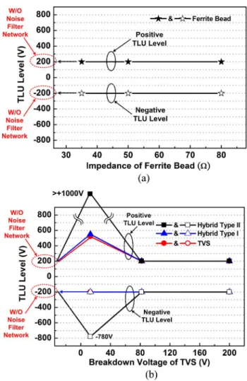
Four other types of noise filter networks, namely, ferrite bead, TVS, hybrid type I, and hybrid type II, are shown in Fig. 13(a)–(d), respectively. Fig. 14(a) and (b) shows their improvements on both positive and negative TLU levels of the SCR test structure.
The ferrite bead can absorb RF energy while the noise-induced transient current flows through it. The resistor-type fer-rite beads with three different minimum impedances at 25 MHz are employed in this paper: 35, 50, and 80 Ω. However, a noise filter network with only ferrite bead does not have an improve-ment on the TLU level due to a lesser energy-absorbing ability at frequencies lower than 10 MHz. As shown in Fig. 14(a), the TLU level of the SCR structure will not be efficiently improved (the magnitudes of both positive and negative TLU levels are all equal to 200 V), even though the minimum impedance of the ferrite bead at 25 MHz is as high as 80 Ω.
TVS, which is commonly used to bypass/decouple high-frequency transient noises, is also considered for its improvement on the TLU immunity of the SCR. The bidirectional-type TVS diodes with three different breakdown voltages VBR’s (±13, ±82, and ±200 V) are used in this paper.
As shown in Fig. 14(b), the TVS components with breakdown voltages of ±82 and ±200 V fail to efficiently improve the TLU level of the SCR (the magnitudes of both positive and negative TLU levels are all equal to 200 V) because TLU occurs prior to the breakdown of the high-VBR TVS. Only
the TVS with a low VBR can effectively enhance the TLU
level. For example, the positive TLU level can be enhanced to +520 V for the TVS with a breakdown voltage of ±13 V. Due to different combinations of material and fabrication method, different TVS components may have different abilities to suppress TLU in CMOS ICs under EFT tests. In this work, one of the typical TVS devices is used to evaluate the immunity of the SCR against TLU, which is compared with the effectiveness of other noise filter networks on TLU immunity. In order to optimize the efficiency of TVS for TLU prevention, the correlations between the VBRof TVS and the intrinsic TLU
level of DUT should be clarified in advance.
Hybrid-type filters consisting of both ferrite bead (minimum impedance of 80 Ω at 25 MHz) and TVS (with different VBR)
are also evaluated for their improvements on the TLU level of the SCR, as shown in Fig. 13(c) and (d). Hybrid types I and II are the counterparts of L- and π-section RC filters where the TVS substitutes for the decoupling capacitor as a low-pass component. Because such higher order hybrid-type filters
Fig. 13. Four types of noise filter networks investigated for their improve-ments on the TLU level of the SCR. (a) Ferrite bead. (b) TVS. (c) Hybrid type I. (d) Hybrid type II.
provide higher insertion loss, they enhance the TLU level of the SCR more significantly than ferrite bead or TVS alone, as shown in Fig. 14(b). For example, hybrid type I with a
low-VBR (±13-V) TVS can enhance the positive TLU level up to
+550 V. For hybrid type II with a low-VBR(±13-V) TVS, the
positive (negative) TLU level can be enhanced to over +1000 V (−780 V).
Fig. 14. Relations between the TLU level of the SCR and (a) minimum impedance of the noise filter network with only ferrite bead, and (b) the breakdown voltage of TVS with noise filter networks of TVS, hybrid type I, and hybrid type II.
C. Discussion
By investigating different types of noise filter networks to find their improvements on TLU levels in Figs. 12 and 14 (where the TLU levels are the corresponding minimum EFT voltages to induce latchup under the measurement setup of Fig. 10 with different noise filter networks), it is found that TVS (hybrid type II) does not improve the negative TLU level as greatly as the first-order capacitor filter (L-section RC filter) does. For example, the negative TLU level can be significantly enhanced to over−1000 V using an L-section RC filter with a decoupling capacitance of 0.1 μF, while the TLU level is
−780 V using the hybrid type II with a low VBR(±13-V) TVS.
Thus, the decoupling capacitor is better than TVS for being a noise-bypassing component in noise filter networks because it not only can enhance the negative TLU level more efficiently but also is compatible to CMOS technology for integrating the noise filter into CMOS chips. Particularly for some TVS com-ponents, fabrication is made by modified processes with special materials. Therefore, it may be difficult to integrate the TVS into the silicon chip due to complex process integration. To further improve the TLU immunity of electronic products, chip-level solutions should be adopted to meet applications with high EFT specifications and reduce the cost of electronic products.
For example, an on-chip power-rail ESD clamp circuit between
VDD and VSS power lines can provide a low impedance path
to efficiently discharge ESD current during ESD stress con-ditions [20]. For CMOS ICs under EFT tests, it may be a solution to apply an on-chip power-rail ESD clamp circuit to suppress electrical transients and avoid an unexpected current into the internal circuits. In on-chip circuit design techniques, some circuits have also been proposed to avoid latchup or to detect EFTs under ESD stress conditions [25], [26]. Chip-level solutions have the advantages of single-chip integration in nanoscale CMOS technology and substantially reduce the total cost of microelectronic products. Therefore, chip-level solutions to meet high EFT specifications for microelectronic products are highly requested by the IC industry.
VI. CONCLUSION
Positive and negative EFT voltage pulses have been identified as the realistic TLU-triggering sources under EFT tests. From the experimental measurements, the specific “swept-back” cur-rent caused by the minority carriers stored within the parasitic PNPN structure of CMOS ICs has been proven to be the cause of TLU. Thus, TLU reliability may still exist in qualified CMOS IC products through the quasi-static latchup test. With understanding of the physical mechanism and experimental verification on TLU, circuit design and layout techniques in CMOS ICs can be developed against TLU events under EFT tests.
The TLU immunity of CMOS ICs under EFT tests can be significantly enhanced by choosing the proper components in each noise filter network. From the experimental results, the decoupling capacitor is better than TVS as a noise-bypassing component in noise filter networks because it not only can enhance the TLU level more efficiently but is also compatible to CMOS technology for integrating the noise filter into chips. The optimal design for enhancements of TLU immunity can be achieved through a clear characterization of TLU prevention from different kinds of board-level noise filters. In addition, chip-level solutions should be further developed to meet the high EFT immunity requirement for microelectronic products.
REFERENCES [1] S. Voldman, Latchup. Hoboken, NJ: Wiley, 2008.
[2] S. Bargstätd-Franke, W. Stadler, K. Esmark, M. Streibl, K. Domanski, H. Gieser, H. Wolf, and W. Bala, “Transient latch-up: Experimental analy-sis and device simulation,” in Proc. EOS/ESD Symp., 2003, pp. 80–87. [3] G. Weiss and D. Young, “Transient-induced latchup testing of CMOS
integrated circuits,” in Proc. EOS/ESD Symp., 1995, pp. 194–198. [4] R. Troutman and H. Zappe, “A transient analysis of latchup in bulk
CMOS,” IEEE Trans. Electron Devices, vol. ED-30, no. 2, pp. 170–179, Feb. 1983.
[5] E. Hamdy and A. Mohsen, “Characterization and modeling of transient latchup in CMOS technology,” in IEDM Tech. Dig., 1983, pp. 172–175. [6] M.-D. Ker and C.-Y. Wu, “Modeling the positive-feedback regenerative
process of CMOS latchup by a positive transient pole method—Part I: Theoretical derivation,” IEEE Trans. Electron Devices, vol. 42, no. 6, pp. 1141–1148, Jun. 1995.
[7] W. Morris, “Latchup in CMOS,” in Proc. IEEE Int. Rel. Phys. Symp., 2003, pp. 76–84.
[8] EMC—Part 4-4: Testing and Measurement Techniques—Electrical Fast
Transient/Burst Immunity Test, IEC 61000-4-4 International Standard,
[9] M.-D. Ker and Y.-Y. Sung, “Hardware/firmware co-design in an 8-bits microcontroller to solve the system-level ESD issue on keyboard,” in
Proc. EOS/ESD Symp., 1999, pp. 352–360.
[10] M.-D. Ker and C.-C. Yen, “Investigation and design of on-chip power-rail ESD clamp circuits without suffering latchup-like failure during system-level ESD test,” IEEE J. Solid-State Circuits, vol. 43, no. 11, pp. 2533– 2545, Nov. 2008.
[11] D. Smith, L. Henry, M. Hogsett, and J. Nuebel, “Sources of impulsive EMI in large server farms,” in Proc. EOS/ESD Symp., 2002, pp. 26–31. [12] D. Smith and A. Wallash, “Electromagnetic interference (EMI) inside a
hard disk driver due to external ESD,” in Proc. EOS/ESD Symp., 2002, pp. 32–36.
[13] Electrostatic Discharge (ESD) Sensitivity Testing—Human Body Model
(HBM), EIA/JEDEC Standard Test Method A114-D, 2006.
[14] Electrostatic Discharge (ESD) Sensitivity Testing—Machine Model (MM), EIA/JEDEC Standard Test Method A115-A, 1997.
[15] Electrostatic Discharge (ESD) Sensitivity Testing—Charge Device Model
(CDM), EIA/JEDEC Standard Test Method C101-C, 2004.
[16] M.-D. Ker and S.-F. Hsu, “Physical mechanism and device simulation on transient-induced latchup in CMOS ICs under system-level ESD test,”
IEEE Trans. Electron Devices, vol. 52, no. 8, pp. 1821–1831, Aug. 2005.
[17] S.-F. Hsu and M.-D. Ker, “Transient-induced latchup dependences on power-pin damping frequency and damping factor in CMOS integrated circuits,” IEEE Trans. Electron Devices, vol. 54, no. 8, pp. 2002–2010, Aug. 2007.
[18] M.-D. Ker and S.-F. Hsu, “Evaluation on board-level noise filter networks to suppress transient-induced latchup in CMOS ICs under system-level ESD test,” IEEE Trans. Electromagn. Compat., vol. 48, no. 1, pp. 161– 171, Feb. 2006.
[19] M. Montrose, Printed Circuit Board Design Techniques for EMC
Compliance. Piscataway, NJ: IEEE Press, 2000.
[20] C.-C. Yen and M.-D. Ker, “Transient-induced latchup in CMOS integrated circuits due to electrical fast transient (EFT) test,” in Proc. IEEE Int. Phys.
Failure Anal. Integr. Circuits Symp., 2007, pp. 11–13.
[21] G. Cerri, R. Leo, and V. Primiani, “Electrical fast-transient: Conducted and radiated disturbance determination by a complete source modeling,”
IEEE Trans. Electromagn. Compat., vol. 43, no. 1, pp. 37–44, Feb. 2001.
[22] M.-D. Ker and S.-F. Hsu, “Component-level measurement for transient-induced latchup in CMOS ICs under system-level ESD considerations,”
IEEE Trans. Device Mater. Rel., vol. 6, no. 3, pp. 461–472, Sep. 2006.
[23] IC Latch-Up Test, EIA/JEDEC Std. no. 78A, 2006.
[24] M.-D. Ker, “Whole-chip ESD protection design with efficient VDD-to-VSS clamp circuit for submicron CMOS VLSI,” IEEE Trans. Electron
Devices, vol. 46, no. 1, pp. 173–183, Jan. 1999.
[25] M.-D. Ker, C.-C. Yen, and P.-C. Shin, “On-chip transient detection circuit for system-level ESD protection in CMOS integrated circuits to meet electromagnetic compatibility regulation,” IEEE Trans. Electromagn.
Compat., vol. 50, no. 1, pp. 13–21, Feb. 2008.
[26] J.-J. Peng, M.-D. Ker, and H.-C. Jiang, “Latchup current self-stop circuit for whole-chip latchup prevention in bulk CMOS integrated circuits,” in
Proc. IEEE ISCAS, 2002, vol. 5, pp. 537–540.
Cheng-Cheng Yen (S’07) received the B.S.
de-gree from the Department of Electrical and Control Engineering and the M.S. degree from the Insti-tute of Electronics, National Chiao Tung University, Hsinchu, Taiwan, in 1998 and 2000, respectively. He is currently working toward the Ph.D. degree in the Nanoelectronics and Gigascale Systems Labora-tory, Institute of Electronics, National Chiao Tung University.
His current research interests include transient detection circuits and IC reliability.
Ming-Dou Ker (S’92–M’94–SM’97–F’08) received
the Ph.D. degree from the Institute of Electronics, National Chiao Tung University (NCTU), Hsinchu, Taiwan, in 1993.
He was the Department Manager with the VLSI Design Division, Computer and Communication Re-search Laboratories, Industrial Technology ReRe-search Institute, Hsinchu. Since 2004, he has been a Full Professor with the Department of Electronics Engi-neering, NCTU, where he is also currently with the Nanoelectronics and Gigascale Systems Laboratory, Institute of Electronics. From 2006 to 2008, he was the Director of the Master Degree Program with the College of Electrical Engineering and Computer Science, NCTU, as well as the Associate Executive Director of the National Sci-ence and Technology Program on System-on-Chip, Taiwan. Since 2008, he has been the Chair Professor and Vice President of I-Shou University, Kaohsiung, Taiwan. He has proposed many inventions to improve the reliability and quality of integrated circuits, which have been granted with 139 U.S. patents and 144 Taiwan patents. He had been invited to teach and/or to consult the reliability and quality design for integrated circuits by hundreds of design houses and semi-conductor companies in the worldwide IC industry. In the field of reliability and quality design for circuits and systems in CMOS technology, he has published over 360 technical papers in international journals and conferences. His current research interests include reliability and quality design for nanoelectronics and gigascale systems, high-speed and mixed-voltage I/O interface circuits, on-glass circuits for system-on-panel applications, and biomimetic circuits and systems for intelligent prosthesis.
Dr. Ker has served as a member of the Technical Program Committee and the Session Chair of numerous international conferences. He was the Associate Editor for the IEEE TRANSACTIONS ONVLSI SYSTEMS. He has been selected as the Distinguished Lecturer in the IEEE Circuits and Systems Society (2006–2007) and in the IEEE Electron Devices Society (2008–2009). He was the President of Foundation in Taiwan ESD Association. Since 2008, he has been elevated as an IEEE Fellow “for his contributions to the electrostatic protection in integrated circuits and the performance optimization of VLSI microsystems.” In 2009, he was awarded as one of the top ten Distinguished Inventors in Taiwan and one of the top hundred Distinguished Inventors in China.
Tung-Yang Chen (S’98–M’02) received the Ph.D.
degree from the Institute of Electronics, National Chiao Tung University, Hsinchu, Taiwan, in 2002.
He was with UMC and worked on advanced ESD devices in different generation processes, including 65 nm, 90 nm, SOI, SiGe, etc., from 2001 to 2003. Since 2003, he has been with Himax Technologies, Inc., Tainan, Taiwan. He has been with Himax for more than six years and worked on full-chip ESD protection design to meet system-level ESD immu-nity. He is currently a Technical Manager with the Basic Technology Department, Research and Development Center, Himax Technologies, to lead the Basic Technology Group on the research of signal integrity, power integrity, EMI, EMS, and ESD immunity. He has proposed many inventions to improve the reliability and quality of integrated circuits and the mass-production process technologies, which have been granted with 12 U.S. patents and 12 Taiwan patents. He has published over 50 technical papers in journals and conferences. He had been invited to teach and/or to consult the reliability and quality design for integrated circuits by many design houses. He was also invited to teach and consult the reliability and yield improvement for the mass-production process of LCM factories by the TFT LCD industry in Taiwan and China.