The Copper Contamination Effect of Al
2O
3Gate
Dielectric on Si
C. C. Liao, C. F. Cheng,zD. S. Yu, and Albert Chin
Department of Electronics Engineering, National Chiao Tung University, Nano Science and Technology Center, University System of Taiwan, Hsinchu, Taiwan
We have studied the Cu contamination effect on 4.2 nm thick Al2O3 metal-oxide semiconductor 共MOS兲 capacitors with an equivalent-oxide thickness共EOT兲 of 1.9 nm. In contrast to the large degradation of gate oxide integrity of control 3.0 nm SiO2 MOS capacitors contaminated by Cu, the 1.9 nm EOT Al2O3MOS devices have good Cu contamination resistance with only small degradation of gate dielectric leakage current, charge-to-breakdown, and stress-induced leakage current. This strong Cu contamination resistance is similar to oxynitride共with high nitrogen content兲, but the Al2O3gate dielectric has the advantage of higher value and lower gate dielectric leakage current.
© 2004 The Electrochemical Society. 关DOI: 10.1149/1.1789391兴 All rights reserved.
Manuscript submitted January 6, 2004; revised manuscript received March 18, 2004. Available electronically September 27, 2004.
To reduce the circuit’s RC delay from back-end metal lines and parasitic capacitors, Cu and low- dielectric are required. However, Cu diffusion into low- and front-end metal-oxide semiconductor field effect transistors共MOSFETs兲 is an important issue.1-12The Cu contamination from back-end Cu interconnects or the back-side wa-fer surface contaminated by Cu accumulates at the Si/SiO2 interface6-8or reacts with Si to form silicide. The precipitate Cu at the oxide interface increases the subthreshold swing of MOSFETs,7,9 shifts the threshold voltage, and degrades the gate leakage current.10-12The Cu silicide also increases the unwanted leakage current in the source-drain junction. To reduce Cu diffusion during back-end thermal cycling, a barrier metal under Cu and thick SiN between each intermetal layer 共IML兲 dielectric are usually added. However, the added SiN of typically 50 nm has a large -value of 7.5 and degrades the total of combined IML dielectric and SiN. The increasing effective is unfavorable because it in-creases the circuit’s back-end resistance-capacitance共RC兲 delay. In this paper, we have studied the Cu contamination effect in high- Al2O3 gate dielectric13-16 with small equivalent-oxide thickness 共EOT兲 of 1.9 nm, where the high- gate dielectric is important for continuously scaling down the nanometer-scale MOSFET. In con-trast to the large degradation of gate oxide integrity in 3.0 nm ther-mal SiO2, the smaller 1.9 nm EOT Al2O3 gate dielectric shows much better resistance to Cu contamination-related degradation on gate dielectric leakage current, charge-to-breakdown (QBD), and stress-induced leakage current 共SILC兲. Therefore, the high- gate dielectric with Al2O3ternary compound such as HfAlO or LaAlO3 should have this additional advantage besides the high- value. This is the first study of Cu diffusion in high- Al2O3.
Experimental
Standard 4 in., p-type Si共100兲 wafers with a typical resistivity of ⬃10 ⍀-cm were used in this study. After standard cleaning, the device active region was formed by thick field oxide and patterning. Then the⬃4.2 nm Al2O3was formed by physical-vapor deposition from an Al2O3sputter source, oxidation at 400°C under O2ambient for 5 min, and annealed at N2 ambient for 25 min. From the capacitance-voltage共C-V兲 measurement, a value of 8.5 and EOT of 1.9 nm were obtained. Then the gate electrode was formed by depositing a 300 nm thick aluminum by thermal evaporation and patterning, where the fabricated area of MOS capacitors is 100 ⫻ 100 m. The Cu contamination to the Al2O3metal-oxide semi-conductor共MOS兲 devices was introduced by contacting the front side of devices into a Cu共NO3)2 solution with 10 ppb or 10 ppm concentration for 1 min followed by driving-in at 400°C N2
anneal-ing. The existence of Cu within gate SiO2 by this contamination process was confirmed by secondary ion mass spectroscopy共SIMS兲 measurements reported previously,11where strong Cu accumulation is observed in both poly-Si and SiO2. A more detailed Cu conta-mination process and discussion of degradation on gate dielectric integrity of SiO2 and SiON can be found in our previous publications.10-12 The Cu contamination effect was studied by current-density and voltage 共J-V兲 measurements in high- Al2O3 gate dielectric MOS capacitors.
Results and Discussion
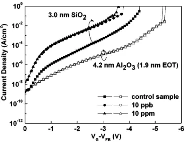
Figure 1 shows the J-(VG-VFB) characteristics of Al2O3 gate capacitors with⬃4.2 nm physical thickness 共1.9 nm EOT兲, where the VFBis the flatband voltage obtained from the C-V measurement and quantum mechanical calculation. The VFBof⫺0.7 and ⫺0.85 V are obtained for Al2O3 and SiO2gate dielectric capacitors, respec-tively. There is no significant VFB change after Cu contamination. This suggests that the Cu may behave as a neutral trap in the gate dielectric, consistent with our previous report.12For comparison, the J-(VG-VFB) characteristics of a 3.0 nm thick SiO2 MOS device were also plotted. For samples without Cu contamination, the 1.9 nm EOT Al2O3gate capacitor has ca. one order of magnitude lower leakage current than 3.0 nm SiO2, which is the fundamental
advan-zE-mail: cfcheng.ee92g@nctu.edu.tw
Figure 1. The J-(VG-VFB) characteristics of MOS capacitors with 4.2 nm
Al2O3gate dielectric共1.9 nm EOT兲 with or without Cu contamination. The
MOS devices with 3.0 nm thermal SiO2are also added for comparison. The
devices were contaminated by 10 ppb or 10 ppm Cu. Journal of The Electrochemical Society, 151共10兲 G693-G696 共2004兲
0013-4651/2004/151共10兲/G693/4/$7.00 © The Electrochemical Society, Inc.
G693
) unless CC License in place (see abstract).
ecsdl.org/site/terms_use
address. Redistribution subject to ECS terms of use (see
140.113.38.11
tage of high- gate dielectric. The Cu contamination in 3.0 nm SiO2 control devices have a significant effect on gate dielectric leakage
current, which was increased by ca. two orders of magnitude. The 10 ppb and 10 ppm Cu-contaminated SiO2 control devices show almost identical leakage current before breakdown voltage (VBD), although the VBDis lower in 10 ppm contaminated devices than the 10 ppb case. Such effect was previously attributed to the Cu trap energy state inside the SiO2dielectric;11the leakage current shows an exponential relation with the trap energy in direct tunneling re-gime with less concentration dependence. In contrast to the large increasing leakage current共two orders of magnitude兲 in SiO2MOS capacitors contaminated by Cu, negligible leakage current increase in Al2O3 MOS capacitors is measured with high 10 ppm Cu con-tamination. The reason the Cu contamination has little effect on the Al2O3 gate dielectric may be due to the strong diffusion barrier property similar to Si3N4, where the Al2O3can even be used as the diffusion barrier for a small H2molecule.17
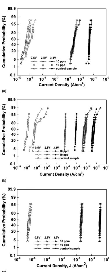
Figure 2a-c further compares the cumulative leakage current dis-tributions of the 4.2 nm Al2O3共1.9 nm EOT兲, 3.0 nm SiO2, and 3.6 nm oxynitride with 23% N content共3.0 nm EOT兲, respectively. The control gate oxide leakage current of 3.0 nm SiO2 MOS device shows an increasing trend by one to two orders of magnitude at 0.5 and 2.5 V bias with increasing Cu concentration from 10 ppb to 10 Figure 2. The distribution of leakage current density for共a兲 4.2 nm Al2O3
gate dielectric共1.9 nm EOT兲, 共b兲 3.0 nm thermal SiO2, and共c兲 3.6 nm SiON
with 23%N content共3.0 nm EOT兲 gate dielectrics with or without Cu con-tamination.
Figure 3. The共a兲 QBDand共b兲 tBDdistribution of 4.2 nm Al2O3gate
dielec-tric共1.9 nm EOT兲 MOS devices under different Cu contamination levels. The distributions of 3.0 nm SiO2MOS capacitors with or without Cu
con-tamination are also added for comparison. Journal of The Electrochemical Society, 151共10兲 G693-G696 共2004兲 G694
) unless CC License in place (see abstract).
ecsdl.org/site/terms_use
address. Redistribution subject to ECS terms of use (see
140.113.38.11
ppm. In sharp contrast, only slightly increasing leakage current at lowest 0.5 V bias can be observed in the 4.2 nm Al2O3 共1.9 nm EOT兲. This increasing leakage current in the pretunneling region at low voltage is also previously observed in thick 5.0 nm SiO2and oxynitride with 16% N content,10-12which is attributed to the trap-assisted tunneling originated by neutral traps formed by Cu inside the oxide matrix. It is noticed that although the degradation of pre-tunneling leakage current is negligible for the 3.6 nm oxynitride with 23% N, the Al2O3still has strong advantage of much smaller EOT of only 1.9 nm than the 3.0 nm EOT oxynitride共23% N兲. In addition, the-value of 8.5 for Al2O3 is also higher than the 4.7 -value for 23% N oxynitride,10which is important for gate dielec-tric application in nanometer-scale MOSFETs.
Figure 3a shows the comparison of QBDdistribution of 4.2 nm Al2O3gate dielectric共1.9 nm EOT兲 with the control 3.0 nm thermal oxide, with or without the Cu contamination. The good quality of control 3.0 nm oxide without contamination is evidenced from the high QBD of ⬃0.13 C/cm2 共⫺4.3 V constant voltage stress兲 and close to the published data.18The Cu contamination effect on SiO2 gate capacitor lowers the QBDwith a wider distribution, which is consistent with the larger distribution of leakage current shown in Fig. 2b. In sharp contrast, the Cu contamination at both 10 ppb and
10 ppm has only small effects on QBDdistribution of the 1.9 nm EOT Al2O3gate dielectric and is free from the trail QBDdistribution devices. This result is also consistent with the tight gate current distribution shown in Fig. 2a. It is noticed that the QBDvalue de-creases rapidly with increasing stress voltage, and the mean QBDof 0.4 C/cm2for 4.2 nm Al2O3gate dielectric, biased at a large voltage of 5.8 V, is also comparable to SiO2within the same order.18This suggests the excellent quality of high- Al2O3gate dielectric. Figure 3b further shows the time-to-breakdown (tBD) plot stressed at⫺4 V at 150°C. The larger tBDdecrease of Cu-contaminated SiO2than that of Al2O3 is due to the larger increase of leakage current in SiO2 after contamination shown in Fig. 1.
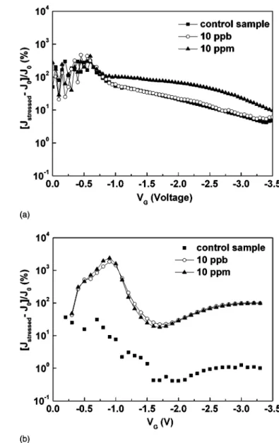
The SILC is another important factor for gate dielectric reliabil-ity evaluation. Figure 4a and b shows the comparison of the stress effect on J-V characteristics for MOS capacitors with 4.2 nm Al2O3 gate dielectric 共1.9 nm EOT兲 and 3.0 nm thermal oxides, respec-tively, with or without Cu contamination. In both cases, the applied stress condition is at⫺3.3 V for 10,000 s. Although the amount of injected charges is less for Al2O3dielectric than SiO2, this is due to the fundamental advantage for high- gate dielectric with largely Figure 4. The stress effect on J-(VG-VFB) characteristics for MOS
capaci-tors contaminated by Cu with共a兲 4.2 nm Al2O3gate dielectric共1.9 nm EOT兲
and共b兲 3.0 nm SiO2. The applied stress condition is at⫺3.3 V for 10,000 s.
Figure 5. The stress and Cu contamination effect on⌬J/J-V characteristics
of共a兲 4.2 nm Al2O3 gate dielectric共1.9 nm EOT兲 and 共b兲 control 3.0 nm
SiO2MOS capacitors.
Journal of The Electrochemical Society, 151共10兲 G693-G696 共2004兲 G695
) unless CC License in place (see abstract).
ecsdl.org/site/terms_use
address. Redistribution subject to ECS terms of use (see
140.113.38.11
improved gate leakage current. Among all the Al2O3and SiO2MOS devices with or without Cu contamination, the control 3.0 nm SiO2 MOS capacitor has the smallest current change and better than the 4.2 nm Al2O3MOS device under the same stress condition. This is due to the robustness of thermal SiO2 where larger bulk oxide and interface defects are usually found in high- dielectric such as Al2O3. The amount of these weak defects increases under charge injection during constant voltage stress, which causes higher leakage current in MOS capacitors.
To further analyze the SILC effect, we have plotted the current change (Jstressed-J0)/J0as a function of bias voltage in Fig. 5, which is more sensitive than the Jstressed-V plot shown in Fig. 4. For the uncontaminated Al2O3and SiO2MOS devices shown in Fig. 5a and b, respectively, the Al2O3dielectric capacitor has higher SILC cur-rent than the SiO2devices, even though the dielectric thickness共4.2 nm兲 for Al2O3is thicker than the SiO2共3.0 nm兲. This is due to the higher bulk and interface defects in high- Al2O3 gate dielectric than thermal SiO2. However, the SILC of⌬J/J0increases rapidly in the SiO2devices even under the smallest Cu contamination of 10 ppb. The increasing SILC with Cu contamination is previously at-tributed to the formation of neutral traps inside the oxide and interface.12In contrast, the⌬J/J0only increases slightly at 10 ppb Cu contamination and the amount of increase at 10 ppm Cu is still less than the SiO2 case. The smaller amount of Cu-contamination-generated SILC in Al2O3gate dielectric suggests the good diffusion barrier property and is also consistent with the smaller degradation on dielectric leakage current and QBDshown in Fig. 1 and 3.
Conclusion
We have studied the Cu contamination effects on gate dielec-tric integrity of 4.2 nm Al2O3 dielectric. By comparing with the control 3.0 nm SiO2 MOS capacitors contaminated by Cu, much smaller degradation of gate dielectric leakage current, QBD and SILC is found in 1.9 nm EOT Al2O3MOS devices. The much better resistance of Cu contamination in ultrathin 1.9 nm EOT Al2O3 MOS capacitor is the strong advantage for high- Al2O3 gate dielectric.
Acknowledgments
This work has been sponsored by National Science Council of the R.O.C. under contract no. NSC92-2215-E-009-031.
The National Chiao Tung University assisted in meeting the publication costs of this article.
References
1. D. A. Ramappa and W. B. Henley, J. Electrochem. Soc., 146, 2258共1999兲. 2. B. Vermeire, L. Lee, and H. G. Parks, IEEE Trans. Semicond. Manuf., 11, 232
共1998兲.
3. P. Motte, J. Torres, J. Palleau, F. Tardif, and H. Bernard, Solid-State Electron., 43, 1015共1999兲.
4. T. Gravier, F. Braud, J. Torres, J. Palleau, A. Chantre, and J. Kirtsch, Microelectron. Eng., 33, 211共1997兲.
5. T. Heiser, S. McHugo, H. Hieslmair, and E. R. Weber, Appl. Phys. Lett., 26, 3576 共1997兲.
6. Y. Shacham-Diamand, A. Dedhia, D. Hoffstetter, and W. G. Oldham, IEEE VMIC Conference, p. 109共1991兲.
7. K. Hozawa, T. Itoga, S. Isomae, J. Yugami, and M. Ohkura, in Symposium on VLSI Technology, p. 24共2000兲.
8. A. Correia, D. Ballutaud, and J. L. Naurice, Jpn. J. Appl. Phys., Part 1, 33, 1217 共1994兲.
9. M. Inohara, H. Sakurai, T. Yamaguchi, H. Tomita, T. Iijima, H. Oyamatsu, T. Nakayama, H. Yoshimura, and Y. Toyoshima, in Symposium on VLSI Technology, pp. 26-27共2000兲.
10. Y. H. Lin, F. M. Pan, Y. C. Liao, Y. C. Chen, I. J. Hsieh, and A. Chin, J. Electro-chem. Soc., 148, G627共2001兲.
11. Y. H. Lin, Y. C. Chen, K. T. Chan, F. M. Pan, I. J. Hsieh, and A. Chin, J. Electro-chem. Soc., 148, F73共2001兲.
12. Y. H. Lin, Y. H. Wu, A. Chin, and F. M. Pan, J. Electrochem. Soc., 147, 4305 共2000兲.
13. C. H. Huang, D. S. Yu, A. Chin, W. J. Chen, C. X. Zhu, M.-F. Li, B. J. Cho, and D. L. Kwong, Tech. Dig. - Int. Electron Devices Meet., 2003, 319.
14. H. Hu, C. Zhu, X. Yu, A. Chin, M. F. Li, B. J. Cho, and D. L. Kwong, IEEE Electron Device Lett., 24, 60共2003兲.
15. A. Chin, C. C. Liao, C. H. Lu, W. J. Chen, and C. Tsai, in Symposium on VLSI Technology, p. 133共1999兲.
16. A. Chin, Y. H. Wu, S. B. Chen, C. C. Liao, and W. J. Chen, in Symposium on VLSI Technology, p. 16共2000兲.
17. D. J. Jung, B. G. Jeon, H. H. Kim, Y. J. Song, B. J. Koo, S. Y. Lee, S. O. Park, Y. W. Park, and K. Kim, Tech. Dig. - Int. Electron Devices Meet., 1999, 279. 18. Y. Taur and T. K. Ning, Fundamental Modern VLSI Devices, p. 106, Cambridge
University Press, New York共1998兲. Journal of The Electrochemical Society, 151共10兲 G693-G696 共2004兲 G696
) unless CC License in place (see abstract).
ecsdl.org/site/terms_use
address. Redistribution subject to ECS terms of use (see
140.113.38.11