IEEE TRANSACTIONS ON ELECTRON DEVICES, VOL. 42, NO. 2, FEBRUARY 1995 307
Characteristics of Self-Induced Lightly-Doped-
Drain Polycrystalline Silicon Thin Film
Transistors with Liquid-Phase Deposition Si02
as Gate-Insulator and Passivation-Layer
Ching-Fa Yeh, Tzung-Zu Yang, and Tai-Ju ChenAbstract- As the passivation layer on the top of undoped offset region for offset-gate structured poly-Si TFTs is exposed to hydrogen plasma, a lightly-doped-like drain region could be equivalently self-induced. The hydrogenated polycrystalline silicon thin-film transistor of this structure, named self-induced lightly-doped-drain (SI-LDD) poly-Si TFTs, was first developed with liquid-phase deposition oxide as both the gate insulator and the passivation layer. This paper describes the optimum hydrogenation condition, and the electrical characteristics for the novel SI-LDD poly-Si TFTs. The effects of DC electrical stress on SI-LDD poly-Si TFTs are also described. Finally a model is proposed to explain the degradation phenomena observed in our SI-LDD devices.
I. INTRODUCTION
OLYCRYSTALLINE silicon thin-film transistors (Poly-
P
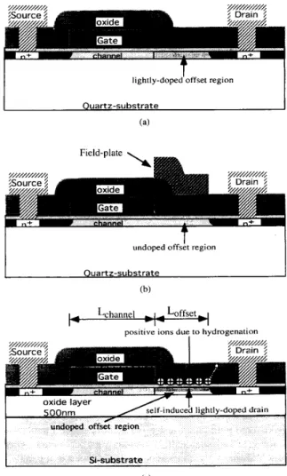
Si TFTs) have been actively investigated for a long time because of their potential use in applications such as three-dimensional integrated circuits and active-matrix liquid- crystal displays (AMLCDs). Because of their high field-effect mobility and reliability, poly-Si TFTs can be used in both the peripheral circuits and switching devices of AMLCDs. However, poly-Si TFTs have an anomalous OFF-state leakage current which increases with gate voltage (VGS) and drain voltage (VDS), and are unacceptable for switching device application. Holding signal levels needed for acceptable image quality requires lowering the OFF-state current below 0.1 pA per micrometer of channel width [l].The anomalous leakage current ( 1 0 ~ ~ ) is generally at- tributed to field enhanced carrier emission via trap states near the drain junction. To decrease the electric field in the drain depletion region, an offset-gate structured TFT (Fig. l(a)) in which a lightly-doped n- region is introduced between
the undoped channel and the n+ region has been proposed
[2]-[4]. In that case, the additionally required implantation for lightly-doped n- region complicates processing and in- creases costs. Besides, another TIT structure called the field- induced-drain (FID) TFT has also been proposed to reduce the anomalous leakage current and achieve high ON/OFF current ratio [5]-[8]. However, this FID structure (Fig. l(b)) requires
Manuscript received May 11, 1994; revised October 4, 1994. The review of this paper was arranged by Associate Editor K. Shenai.
The authors are with the Department of Electronics Engineering & Institute of Electronics, National Chiao-Tung University, Hsinchu, Taiwan, R.O.C.
IEEE Log Number 9407766.
I
lightly-doped offset region
Ouartz-substrate
(a)
I
undoped offset region
Ouartz-substrate
(b)
+ Lchannel
q+
Loffset4
positive ions due to hydrogenationI
oxide layer(c)
Fig. 1. (a) Offset-gate TFT structure; (b) field-induced-drain (FID) TFT structure; (c) self-induced lightly-doped-drain (SI-LDD) TFT structure.
use of an additional field-plate electrode. Furthermore, the performance of the FID device is very sensitive to the field- plate bias and interlayer material compositional characteristic. Recently, Kanicki [9] proposed a novel TFT with an un- doped offset structure for achieving high ON/OFF current ratio
ydrogenation time Active poly-Si (W thickness (nm) A 0 100 B 3 100 C 3 30 vth S PFE Nt
(v)
(V/dec) (cm2N.sec) (cm-2) 12.9 2.11 17.9 7 . 2 5 ~ 1 0 1 ~ 6.91 1.28 25.5 4 . 2 0 ~ 1 0 1 ~ 3.37 0.425 22.4 3 . 0 0 ~ 1 0 1 ~independent of gate bias. With a dual passivation layer on top of the undoped offset region being exposed to hydrogen plasma, a lightly-doped-like region can be equivalently self- induced. The dual passivation layer was prepared by a series of processes including silicon dioxide (SiOz) deposition by plasma enhanced chemical vapor deposition (PECVD), hydro- gen plasma annealing and N-rich silicon nitride deposition by PECVD. These processes were very complicated, and the equipment was very expensive. In this study, we first developed an undoped poly-Si TFT structure with liquid-phase deposited (LPD) [ 101 oxide as a gate insulator and passivation layer. The apparatus used for LPD-oxide was very inexpen- sive, and the process easily performed at room-temperature. Because the hydrogenation treatment is an indispensable step in poly-Si TFTs processing, we called such devices “Self- Induced Lightly-Doped-Drain’’ (SI-LDD) poly-Si TFTs (Fig. l(c)) [ l I], [12]. First, we will describe the investigation of the hydrogenation condition for the passivation layer, and then describe the electrical behavior of our SI-LDD poly-Si TFTs. The effects of DC electrical stress on the new devices will also be described. Finally, a model of SI-LDD and the migration of positive charges will be proposed to explain the results of this research.
11. DEVICE FABRICATION
The fundamental fabrication processes of SI-LDD TFTs are compatible with those of conventional TFTs. First, both the 30 nm and the 100 nm-thick active poly-Si layer prepared by solid-phase crystallization (SPC) method were patterned into islands, respectively. As both gate insulator and passivation layer, a 100 nm-thick silicon oxide was grown at 30°C by LPD method. The 400 nm-thick poly-Si layer was deposited and patterned as a gate electrode. After the undoped offset regions were covered with photo-resist, the self-aligned ion implanta- tion for gate and sourceldrain regions was performed. After dopant activation, hydrogenation was performed in a parallel- plate plasma reactor at 300°C. The optimum hydrogenation time was determined. Finally, a 500 nm-thick interlayer oxide was formed by PECVD method. After metallization, sintering was performed at 400°C for 15 minutes. The maximum process temperature was 625°C. A schematic cross-sectional view of a finished SI-LDD poly-Si TFT is shown in Fig. l(c). In this experiment, the channel length ( L ) is 20 pm,
the channel width ( W ) is 100 pm, and the offset length (L,tf)
varies from 0 to 10 pm. Three groups of SI-LDD samples labeled A, B and C were prepared and are summarized in Table I.
To reduce the series resistance in the undoped offset region, the hydrogenation treatment must be optimized; that is, enough positive charges must be incorporated into the passivation layer to ensure that an adequate number of electrons will be induced in the surface layer of the offset region. Hydrogenation was performed in a atmosphere containing H2 and N2 gas mixture. As a parameter, the hydrogenation time was 1 hour, 2 hours, or 3 hours. To trace the effect of hydrogenation
on incorporation of positive charges, the metdoxidelsingle- crystal Si (MOS) capacitors with hydrogenated LPD-Si02 as insulator were also prepared.
111. RESULTS AND DISCUSSION
A. Hydrogenation Effect
First, the positive-charge incorporation in the passivation layer was investigated by means of flat-band voltage (VFB) shifts of MOS capacitors exposed to hydrogen plasma. As shown in Fig. 2, the value of VFB corresponding to C-V curves changed from -10.6 V to -20.2 V and to -24.2 V after 1 hr and 2 hrs of hydrogenation, respectively. These results show that positive charges indeed were incorporated in the passivation layer during hydrogenation. There is also evidence of positive charges incorporated in the passivation layer of SI-LDD poly-Si TFT: it became more conductive owing to electron accumulation on the surface layer of the undoped offset region. In other words, a lightly-doped-like region has been equivalently self-induced with the hydrogen plasma treatment. The quantity of positive charges is propositional to hydrogenation time. However, the VFB changes indicated a saturation after 2 hrs. of hydrogenation. As shown in Fig. 3, there is also evidence of saturation on normalized ON current ( I O N ) in SI-LDD poly-Si TFTs which can be attributed to positive-charge saturation in the passivation layer. Therefore, in this study, we considered 3 hours the optimum hydrogenation time.
B. Characteristics of Low-Temperature-Processed (LTPISI-LDD Poly-Si TFTS
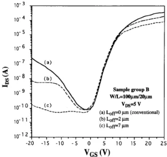
Next, we will discuss the characteristics of the LTP SI-LDD poly-Si TFTs with LPD-Si02 as gate insulator. Figure 4 shows the transfer characteristics ( 1 ~ s - v ~ ~ ) at
VDS
=5 V for the group A samples (no hydrogenation) with L,tf as a parameter. From the 1 ~ s - v ~ ~ of the conventional TFT (L,E =O pm), the typical characteristic parameters including threshold voltage (Vth) of 12.9 V, subthreshold swing (S) of 2.11 Vldec,YEH et al.: CHARACTERISTICS OF SELF-INDUCED LIGHTLY-DOPED-DRAIN POLYCRYSTALLINE SILICON 309
Y
U 1.1 Before1
Hydrogenation 1.0-.
0.9-
0.8
-
Hydrogenation 2 h n 0.7-
0.6-
0.5-
0 . 4 ! . I ., .
I . I . I . I . I-
I .I
-40 - 3 5 - 3 0 - 2 5 - 2 0 -15 - 1 0 - 5 0 5V
Fig. 2. High frequency (1 MHz) C-V characteristics and flat-band voltage
(VFB) of MOS capacitors before and after hydrogenation. The value of VFF~
corresponding to C-V curves changed from - 10.6 V to -20.2 V and to -24.2 Vafter 1 hr and 2 hrs of hydrogenation, respectively.
3
.$330
20
i5
100
U Lo@ pm (conventional) A L,@pm --c- L , ~ l O p m0
1
2
3
4
5
6
Hydrogenation Time (hrs)
Fig. 3. Normalized ON current ( I O N ) as a function of hydrogenation time for SI-LDD poly-Si TFTs with Lon =0 pm, 5 p m and 10 pm. Normalized ION saturated after 2 hrs of hydrogenation for TFTs with lo^ =5 p m , and 10 pm.
mobility FE) of 17.9 cm2N.sec and trap-state density ( N t )
of 7.25 x 10l2 cmP2 were obtained and summarized in Table I. Vth is defined as the gate voltage which yields a normalized drain current of 0.1 pA.W/L measured at VDS =5 V 1131. Nt existed in the poly-Si channel is calculated by extracting a straight line on the plot of In ( 1 ~ s / V & ) versus llV& at low VDS and high V&j [14]. Since the group A were as-fabricated samples, no self-induced lightly-doped drain existed; ON-state performance was very poor and severely limited by the series
10-
Sample group A
OFF-state leakage current
-20 - 1 5 -10 - 5 0 5 10 15 20 25
VGS
(v)
Fig. 4. A typical I u s - L i ; ~ characteristics at L D s =5 V for sample group A
poly-Si TITS with Lon as a parameter.
resistance in undoped offset region. On the other hand, for TFT with Loff = 2 pm or 7 pm, the OFF-state current increased with lV&l in the range of -10 V
<
VGS<
0 V. The behavior was similar to that in conventional poly-Si TFT. The OFF- state current in this gate bias range was dominated by the resistive leakage current [lo], [15]. The increase of negative VGS reduces the resistance of the channel region, as a result, the resistive leakage current increases.Figures 5(a), (b) and (c) show typical output characteristics ( 1 ~ s - v ~ ~ ) for sample group A with L,ff =0 pm, 2 pm and 7 pm, respectively. Except for conventional TFT
lo^
=O pm), both offset-gate structured TFTs showed triode-like character- istics in the low VDS region. In other words, the TFTs without hydrogenation suffered from the so-called current-pinching phenomena in the low VDs region. It is attributable to high series resistance in the undoped offset region.However, a comparison of Fig. 6 (sample group B) with Fig. 4 shows 3 hours of hydrogenation time greatly improves transfer characteristics. When compared to the transfer charac- teristics of traditional TFT, significantly improved parameters including Vth of 6.91 V, S of 1.28 Vldec, ,LLFE of 25.5
cm2N.sec and Nt of 4.2 x
lo1'
cm-2 were obtained; these are summarized in Table I. And, after 3 hrs. of hydrogenation the driving currents were increased over two orders of magnitude no matter whether the TFT was tested with L,ff of 2 pm or 7 pm. Because a lightly-doped-drain had been induced and thus the conductivity was increased, these samples were therefore called SI-LDD TFTs. Moreover, in these SI-LDD TFTs, excellent turn-on characteristics without kink effect, as shown in Fig. 7(a), (b) and (c), were also achieved. The saturation current ID^,+^^) only decreased a little even when the TFT was tested with Loff of 7 pm. And the saturation voltage (VDS,Sat) also increased with L,E. On the other hand, from a comparison of Fig. 4 and Fig. 6 we see that in our LTP SI-LDD poly-Si TFTs, the L,ff of 2 pm was not long310 IEEE TRANSACTIONS ON ELECTRON DEVICES, VOL. 42, NO. 2 , FEBRUARY 1995 o.2$ n U
%
J 1.2- 0.9-
VGS= 6 V I . 0 5 10 1 5 20 25 3 80.0 , 60.0-
n v) 0 5 10 15 20 25 VDS(v)
(c)Fig. 5. A typical output characteristics ( 1 0 s - V ~ ~ ) with \&bas a parameter for sample group A. (a) Lon =O pm (conventional), (b) Lon =2 pm, and
(c) L,E =7 pm. 10-3
6
_---
.---
1 0 -1 2 4 . -20 - 1 5 -10 - 5 0 5 10 15 20 VGS(v)
Fig. 6. A typical transfer characteristics ( l ~ . ; - V c s ) at VDS =5 V for sample
group B with Lon as a parameter.
enough to make OFF-state current independent of ~ V G S ~ for both sample groups A and B.
From Fig. 6, we see that the minimum OFF-state current of
about lo-'' A is still too large to satisfy the specification of less than 0.1 pA per micrometer of channel width for switching- device application in AMLCD. To further improve ON/OFF electric characteristics, the effectness of thinning the active poly-Si films was also investigated for the SI-LDD TFTs. Fig. 8 shows a typical transfer characteristics of VDS =5 V for the sample group C, in which the active poly-Si was 30 nm-thick. Compared with sample groups A and B, we found that the sample group C indeed had much-improved OFF-state characteristics. Especially, the minimum OFF-state drain current drops to about 2 PA. It shows that our SI-LDD TFTs with thinned poly-Si film achieves the specification of AMLCD. On the other hand, ON-state current of this sample group with
lo^
=7 pm was decreased about one order of magnitude compared with conventional TFT. Compromising OFF-state current with ON-state current, the offset length in 2-5 pm is therefore an optimum choice for SI-LDD poly-Si TFTs in sample group C . The characteristics parameters of LTP SI-LDD poly-Si TFT with 30 nm-thick active-layer andlo^
=2 pm are summarized in Table I. The characteristics with &h of 3.31 V, S of 425 mV/dec, FE of 22.4 cm'N.sec,Nt of 3.0 x
lo1'
cm-' and IONIIOFF ratio of 2.08 x lo7 at VDS =5 V were obtained. All of the parameters exhibited eminently satisfactory performance. The excellent ON/OFF current ratio (>lo7), nearly independent of VDS and VGS, was achieved.C. Reliability of SI-LDD Poly-Si TFT
The stability of the new SI-LDD poly-Si TFTs is of signifi- cant importance from the standpoints of fabrication technology and device structure. The long-term stability of the devices
YEH et al.: CHARACTERISTICS OF SELF-INDUCED LIGHTLY-DOPED-DRAIN POLYCRYSTALLINE SILICON 311 vGS' 12
v
10.0 0.0 0 5 10 1 5 20 25 3 VDS(VI
(a) 40.0 n 30.0 v9
g
20.0-
10.0 0.0 0 5 10 1 5 20 25 30 VDS(v)
(C)Fig. 7. A typical output characteristics ( 1 ~ s - v ~ ~ ) with I.ksas a parameter for sample group B. (a) Lou =O p m (conventional), (b) L,R =2 pm, and (c) L,tf =7 bm. n
s
a"
U 1 0 - ~ Sample group C WL=lOOpm/U)pn 10-l2, ., .
I , I.
I.
I.
I.
I.
, .
- 2 0 - 1 5 -10 - 5 0 5 1 0 1 5 20 2 5 VGS(v)
Fig. 8. A typical transfer characteristics (ID.;-\,?;S) at IDS =5 V for sample
group C with L,R as a parameter.
after they were fabricated and stored for a long time was studied. We found no changes in the device performance even after two months of storage at room temperature. However, after DC electrical stress, the characteristics of the devices changed significantly.
Fig. 9 shows a typical change of 1 ~ s - v ~ ~ characteristics for the SI-LDD poly-Si TFT (sample group C) with Loff =2
pm under positive stress with VGS =20 V and V& = 0 V for 1.23 x
lo5
s. It is seen that the characteristics curve after positive stress parallelly shifted to the left of the original curve. It is also found that the value of threshold voltage decreased from 3.59 V to 2.28 V, while the subthreshold swing was nearly unchanged. The degradation implied that there existes an instability factor that causes curve parallel shifting. The instability factor obviously can not be attributed to the generation of trapping states. In addition, the minimun of OFF- state current decreased from 7.0 x 10-l' A to 1.8 xA, which was the level of the gate leakage current. The OFF-
state current also increased with IVGS~ and behaved like that in conventional TFTs without offset regions. The degradation phenomenon implied that the series resistance of the current path had increased. The result is consistent with the output Characteristics after stress, which exhibited slight current- pinching phenomena in the linear region at low drain voltage. Figure 10 shows a typical change of 1 ~ s - v ~ ~ characteristics for the same devices (sample group C) after negative stress with VGS = -20 V and VDS =0 V for 2.72 x lo5 S. We can see that device characteristics changed very much after negative stress in comparison with their before-stress values, and they changed differently than after positive stress. The ION after negative stress was significantly suppressed, it was suspected that the series resistance had increased. On the contrary, the OFF-state current (hole current) increased greatly in comparison with that before stress. The increase of minimum OFF-state leakage current was again attributed to the
n
4
v)
n
UStress Condition: vGS=20v, VDs=OV io -3 10 -4
-
Stress Time: 1 . 2 3 ~ 1 6 S 10-5- vDs=lOv
-
-
-
-
-
I ' I ' I-
I ' I ' I ' I-
I-
-20 -15 -10 -5 0 5 10 15 20Fig. 9. A typical change of I D S - V ~ S characteristics for the SI-LDD poly-Si
TFTs with L,~I =2 p m (sample group C) under the stress with VGS =20 V and I'Ds = 0 V for 1.23 x lo5 s.
Stress Condition: v G s = - 2 o v , V,@V
/
n4
10-1 2 3 3 -20 -15 -10 -5 0 5 10 15 20 25Fig. 10. The changes of I D S - \ ~ S characteristics for the SI-LDD poly-Si
TFTs with L,fi = 2 2 p m (sample group C) under the stress with \ ~ / c , s = -20
V and VDS =O V for 2.72 x lo5 s.
series resistance of the current path, which must have locally decreased very much. The above results lead to suspicion that the positive charges in the gate oxide and the passivation layer above the offset region moved differently under both cases of high field stress. The details will be explained later.
To further clear the essential factor of device degradation, the bias-temperature (BT) test on the conventional poly-Si
TFTs without offset region was also studied. The conventional device was also prepared with plasma-treated LPD-oxide as gate insulator. First, after the stress with VGS =20 V at 150°C for 30 min, the transfer curve parallelly shifted to the left about 5 V. The subthrethold swing was nearly unchanged, Next, after the subsequent stress with VGS = -20 V at 15OOC for 30 min, the curve returned about 2.5 V, and the subthrethold swing increased. The value of threshold voltage also changed in response to the shift. The most possible mechanism that could change the performance of our SI-LDD TFTs under stress was the migration of positive charges in the oxide layer [16], [17]. We speculated that most of the positive charges were hydrogen atoms. During the hydrogenation treatment, there were positive charges incorporated in the passivation layer. Because the oxides regarded as paths for high diffusion of hydrogen [ 181, the hydrogen atoms could laterally diffuse into gate oxide. Therefore, many hydrogen atoms acumulated at the poly-Si/SiO2 interface [19]. During stressing at VGS = 20 V, the parallel shift toward the left for the transfer curve implied that the positive charges in the gate dielectric moved more near the poly-Si/SiO2 interface. During subsequently stressing at V& = -20 V, the fact that the transfer curve returned toward the right suggested that the positive charges moved far away from the poly-Si/Si02 interface. In addition, some of the positive charges passivating the traps broke away from the defect sites caused by the high negative gate bias leading to the increase of the effective trap states density ( N t ) [17], [20]. The tests implied that a possible migration phenomenon of positive charges in the plasma-treated LPD- oxide had occurred corresponding to the BT stress. In addition, because no changes in subthreshold swing were found in the
BT tests, we could conclude that neither hot-carrier effect nor charge trapping in the gate dielectric [21-251 dominated the device degradation.
D.
A Proposed ModelAccording to the above discussion, the most probable factor responsible for degradation in the performance of our SI-LDD TFT under stress was the migration of positive charges in the oxide layer. There have been many reports describing the unreliable positive charges existing in insulators [ 161, [17]. We proposed a model and illustrated the mechanism of SI-LDD and degradation in terms of positive charges migration. Figure 1 l(a) shows an original distribution of positive charges incorporated in both the gate oxide and the passivation layer above the offset region after hydrogen plasma treatment. Owing to the existance of positive charges in the passivation layer, beneath it a lightly doped N - layer in the offset region was easily generated. Thus the TFT device with an equivalently lightly-doped offset region could effectively reduce the anomalous leakage current and achieve a high ON/OFF current ratio.
When a positive stress-bias was applied to the gate elec- trode, the high electric field under the gate electrode with the fringing fields at the edge of the gate electrode could make the positive charges migrate. The positive charges in the gate oxide under the gate electrode, as shown in Fig. ll(b), were
~
YEH et al.: CHARACTERISTICS OF SELF-INDUCED LIGHTLY-DOPED-DRAIN POLYCRYSTALLINE SILICON
N- Channel
\
313 N+ Drain<
Passivation Layer N A B C Channel N+ Drain Passivation Layerl \
I Gate Passivation Layer @@@@e@@ @@@@@e@ LPDSiOz+
@W@@@@forced closer to the Si/SiOp interface, therefore the transfer curve at ON state (as shown in Fig. 9) parallelly shifted a little. In addition, the fringing fields will be significant for only a small portion of L,E, a small portion of the positive charges
in the passivation layer were also piled up a short distance away from the gate as shown in Fig. 1 l(b). It can thus be concluded that the positive charges above offset region A were depleted, while those were accumulated above offset region B. Above offset region C, the positive charges were only slightly affected. Therefore, the equivalent resistance ( R 0 ~ A ) at region A increased due to low electron induction; while the equivalent resistance ( R,R B) at region B decreased due to higher electron
induction. The increase in total offset resistance resultantly caused a reduction in the minimun OFF-state current (hole current) and a current-pinching phenomenon in the output characteristics. In addition, the lateral electric field along offset region B also changed with the redistribution of the positive charges. These changes thus caused an increase with ~ V G S ~ in OFF-state current [15]. Therefore the change of transfer curve at OFF state became much different from the simply parallel shift on the conventional device.
On the other hand, when a negative stress-bias was applied to the gate electrode, a high electric field made the distribution of positive charges under the gate electrode and above the offset region change as shown in Fig. ll(c). Owing to the negative electrical field, positive charges easily accumulated above the offset region A, while those were depleted above the offset region B and C. Thus, R o f f ~ easily decreased due to more electrons induced, while R,RB and R o ~ c in- creased greatly due to fewer electrons induced. Therefore, after negative stress the minimun of OFF-state current (hole current) increased with the reduction of total offset resistance. Because the redistribution of positive charges could affect the distribution of the lateral electric field along the offset region, the electric field near offset region A was enhanced. In addition, since these TFTs have been hydrogenated and hydrogen is only weakly bounded to the defect sites, we can see an increase in trap formation as the hydrogen breaks away from weakly passivated defect sites and migrates to the gate electrode. Thus the increase of OFF-state current with ~ V G S ~
was mainly due to the increase of effective trap state density and the lateral electric field along the offset region [15]. At the same time, the ON-state current was limited by the high series resistance in the offset region and effective trap state density. The drain voltage could also play an important role in the degradation of SI-LDD poly-Si TFT. When the drain bias was applied during stress, the carrier-induced metastable midgap states were created within the poly-Si active layer due to the presence of high carrier densities in the channel [21], [23]. However, the enhancement of the high carrier densities on degradation would become dominant only in the case of long stress time.
IV. CONCLUSION
For reducing OFF-state current and achieving high ON/OFF current ratio, a novel and simple SI-LDD poly-Si TFT with LPD-oxide as both gate insulator and passivation layer has been newly developed using LTP technologies. The 3-hour hy- drogenation treatment effectively incorporated positive charges in the passivation layer, and achieved significant improve- ments in device performance, for example, excellent turn-on characteristics without kink effect. The driving currents were increased over two orders of magnitude, while the OFF-state current become independent of ~ V G S ~ (if Loff
>
2 pm).Besides, the SI-LDD poly-Si TFTs with 30 nm-thick active- layer and 2 pm of lo^, having an I ~ ~ J I I o F F ratio of 2.08 x
lo7
at V& =5 V, a /LFE of 22.4 cm2N.sec, a S of 425 mVIdec, aKk,
of 3.37 V, and a Nt of 3.0 x 10l2 cm-' exhibited sufficient performance for pixel transistors of AMLCDs. This new SI-LDD poly-Si TFT’ was rather stable during storage. However, degradation in electrical characteristics owing to migration of
positive charges was found.
ACKNOWLEDGMENT
This study was supported by the National Science Council, Republic of China, under contract number NSC 83-0404-E-
009-093, and partly by Microelectric Technology Development Project, ERSOATRI.
REFERENCES
H. Ohshima and S. Morozumi, “High performance poly-Si TFT for LCDs,” Extended Abstr. 199I Con$ Solid State Devices and Materials,
S. Seki, 0. Kogure, and B. Tsujiyama, “Leakage current characteris- tics of offset-gate-structure polycrystalline-silicon MOSFET’s,” IEEE
Electron Device Lett., vol. 8, no. 9, p. 434, 1987.
K. Tanaka, H. Arai, and S. Kohda, “characteristics of offset-structure polycrystalline-silicon thin-film transistors,” IEEE Electron Device Lert., vol. 9, no. I , p. 23, 1988.
K. Nakazawa, K. Tanaka, S. Suyama, K. Kato, and S. Kohda, “lightly doped drain TlT structure for poly-Si LCDs,” SID Digest, p. 3 11, 1990.
T. Y. Huang, I.-W. Wu, A. G. Lewis, A. Chiang, and R. H. Bruce, “A simpler 100-V polysilicon TFT with improved turn-on characteristics,’’
IEEE Electron Device Lett., vol. 11, no. 6, p. 244, 1990.
T. Y. Huang, 1.-W. Wu, A. G. Lewis, A. Chiang, and R. H. Bruce, “Device sensitivity of field-plated polysilicon high-voltage TFT’s and their application to low-voltage operation,” IEEE Electron Device Lett., vol. 11, no. 11, p. 541, 1990.
K. Takana, S. Suyama, K. Kato, and S. Kohda, “A novel unified- structure field-induced-drain ( W I D ) poly-Si TFTs in CMOS circuits for LCD applications,” SID Digest, p. 539, 1991.
K. Takana, K. Nakazawa, S. Suyama, and K. Kato, “characteristics of field-induced-drain (FID) poly-Si TIT’S with high ON/OFF current ratio,” IEEE Trans. Electron Devices, vol. 39, no. 4, p. 916, 1992. J. Kanicki and M. K. Hatalis, “A simple polysilicon thin film transistor structure for achieving high o d o f f current ratio independent of gate bias,” Extended Abstr. I992 Con$ Solid State Devices and Materials, p. 52.
C . F. Yeh, S. S. Lin, T. Z. Yang, C. L. Chen, and Y. C. Yang, “Perfor-
mance and off-state current mechanism of low-temperature processed polysilicon thin-film transistors with LPD-Si02 gate insulator,” IEEE
Trans. Electron Devices, vol. 41, no. 2, p. 173, 1994.
C. F. Yeh, T. J. Chen, T. Z. Yang, and H. K. Chen, “Low-temperature processed poly-Si TlT with self-induced lightly-doped-drain (SI-LDD) structure,” Electronic Devices and Materials Symposium, (Taiwan), p. 5 ,
Oct. 15-17, 1993.
C. F. Yeh, T. J. Chen, and T. Z. Yang, “DC reliability of low-temperature self-induced lightly-doped drain poly-Si TFTs,” Active Matrix Liquid
Crystal Display Symposium (AMLCDS), (Bethlehem, Pennsylvania), p.
64, Oct. 21-22, 1993.
A. G . Lewis, 1.-W. Wu, T. Y. Huang, M. Koyanagi, A. Chiang, and R. H. Bruce, “Polysilicon thin film transistors for analogue circuit applications,” IEDM Tech. Dig., p. 260, 1988.
J. Levinsor, F. R. Shepherd, P. J Scanlon, W. D. Westwood, G. Este, and M. Rider, “Conductivity behavior in polycrystalline semiconductor thin film transistors,” J. Appl. Phy., vol. 53, no. 2, p. 1193, 1982.
C. F. Yeh, T. Z. Yang, C. L. Chen, T. J. Chen, and Y. C. Yang, “Ex- perimental comparison of off-state current between high-temperature- and low-temperature-processed undoped channel polysilicon thin-film transistors.” JDn. J. A D D ~ . Phvs.. vol. 32. no. IO. D. 4472. 1993. p. 577.
transistor bv hieh-gate-voltage stress,” IEEE Electron Device Lett., vol. <
- -
12, no. 12, p. 676, 1991.
1201 S. Baneriee. H. Shichiio, R. Sundaresan, and S. Mahi. “Hot-electron
-~
degradation of n-channel polysilicon MOSFET’s,” IEEE Trans. Electron
Devices, vol. 35, no. 2, p. 152, 1988.
[21] I.-W.Wu, W. B. Jackson, T. Y. Huang, A. G. Lewis, and A. Chiang, “Mechanism of device degradation in n- and p-channel polysilicon
T l T s by electrical stressing,” IEEE Electron Device Lett., vol. 11, no.
4, p. 167, 1990.
[22] C. A. Dimitriadis and P. A. Coxon, “Effects of temperature and electrical stress on the performance of thin-film transistors fabricated from undoped low-pressure chemical vapor deposited polycrystalline silicon,” Appl. Phys. Lett., vol. 54, no. 7, p. 620, 1989.
[23] M. Hack, A. G. Lewis, and 1.-W. Wu, “Physical models for degrada- tion effects in polysilicon thin-film transistors,” IEEE Trans. Electron
Devices, vol. 40, no. 5, p. 890, 1993.
[24] I.-C. Chen, S. Holland, and C. Hu, “Electrical breakdown in thin gate and tunneling oxides,” IEEE Trans. Electron Devices, vol. 32, no. 2, p. 413, 1985.
[25] N. Kato, T. Yamada, S. Yamada, T. Nakamura, and T. Hamano, “Degradation mechanism of polysilicon TFT’s under d.c. stress,’’ IEDM
Tech. Dig., p. 677, 1992.
Ching-Fa Yeh was born in Hsinchu, Taiwan, on September 20, 1948. He received the B.S. degree from National Oceanic University, Keelung, T a - wan, ROC, in 1971, the M.S. and Ph.D. degrees from the University of Tokyo, Tokyo, Japan, in 1979 and 1982, respectively, all in electrical engineering. From 1982 to 1988, he was with the Fuji Xerox’s Electronic Technology Laboratories, Ebina, where his work has been concerned with the research and development of sermconductor process technologies and devices, particularly on Dry Process technology and Contact Amorphous-Si Image Sensor, and High-Voltage MOSFET.
Currently, he is an Associated Professor at the Department of electronics Engineering & Institute of Electronics, National Chiao-Tung University, Hsinchu, Taiwan. His current research interests include thin-film transis- tor, power devices, silicon-wafer directly bonding technologies, and low- temperature processed materials and devices.
Dr. Yeh is a member of Japanese Journal Applied Physics Society, and he also as an oversea member of program committee of the international Conference on Solid State Devices and Materials.
Tzung-Zu Yang was born in Pingtung, Taiwan, on July 11, 1969. He received the B.S. and M.S. degrees in electronics engineering from National Chiao-Tung University in 1991 and 1993, respectively.
Currently, he is working with the Electronic Research and Service Organization, Industrial Technology Research Institute, Hsinchu, Taiwan, ROC, where he is engaged in the research of field emission display.
..
,1 R. M. PatrikL, R. Lal, and J. Vasi, “Net posithe-charge buildup in various MOS insulators due to high-field stressing,” IEEE Electron
Device Letf., vol. 14, no. 11, p. 530, 1993.
1171 W. B. Jackson, N. M. Johnson, C. C. Tsai, L W . Wu, A. Chiang, and D. Smith, “Hydrogen diffusion in polycrystalline silicon thin films,” Appl.
Phys. Leti., vol. 61, no. 14, p. 1670, 1992.
[18] M. Nakabayashi, M. Ikegami, and T. Daikoku, “Influence of hydrogen on electrical characteristics of poly-Si resistor,” Jpn. J. Appl. Phys., vol. 32, no. 9A, p. 3734, 1993.
[I91 C. A. Dimitnadis, P. A. Coxon, A. J. Lowe, J. Stoemenos, and N. A. Economou, “Control of the performance of polysilicon thin-film
Tai-Ju Chen was born in Tainan, Taiwan, on September 13, 1970 He received the B S. degree in electrical engineenng from National Cheng Kung University, Tainan, Taiwan, ROC, in 1992. He is currently working towards the Ph.D. degree in electronics engineering at National Chiao-Tung University.
His current research interest is in the fabrication of polysilicon thin-film transistors.