Channelwidth dependence of lowfrequency noise in process tensilestrained n
-channel metal-oxide-semiconductor transistors
Ming-Pei Lu, Wen-Chin Lee, and Ming-Jer Chen
Citation: Applied Physics Letters 88, 063511 (2006); doi: 10.1063/1.2172287 View online: http://dx.doi.org/10.1063/1.2172287
View Table of Contents: http://scitation.aip.org/content/aip/journal/apl/88/6?ver=pdfcov
Published by the AIP Publishing
Articles you may be interested in
Role of shallow Si / SiO 2 interface states on high frequency channel noise in n -channel metal-oxide-semiconductor field effect transistors
Appl. Phys. Lett. 95, 123508 (2009); 10.1063/1.3231924
Low temperature mobility in hafnium-oxide gated germanium p -channel metal-oxide-semiconductor field-effect transistors
Appl. Phys. Lett. 91, 263512 (2007); 10.1063/1.2828134
On the beneficial impact of tensile-strained silicon substrates on the low-frequency noise of n -channel metal-oxide-semiconductor transistors
Appl. Phys. Lett. 86, 223509 (2005); 10.1063/1.1942631
Correlation between the 1 f noise parameters and the effective lowfield mobility in Hf O 2 gate dielectric n -channel metal–oxide–semiconductor field-effect transistors
Appl. Phys. Lett. 85, 1057 (2004); 10.1063/1.1779967
A study on interface and charge trapping properties of nitrided n -channel metal-oxide-semiconductor field-effect transistors by backsurface argon bombardment
J. Appl. Phys. 82, 1947 (1997); 10.1063/1.366007
This article is copyrighted as indicated in the article. Reuse of AIP content is subject to the terms at: http://scitation.aip.org/termsconditions. Downloaded to IP: 140.113.38.11 On: Thu, 01 May 2014 02:08:31
Channel-width dependence of low-frequency noise in process
tensile-strained n-channel metal-oxide-semiconductor transistors
Ming-Pei Lu
Department of Electronics Engineering, National Chiao Tung University, Hsin-Chu, Taiwan, Republic of China
Wen-Chin Lee
Exploratory Technology Development-1 Department, Taiwan Semiconductor Manufacturing Company, Hsin-Chu, Taiwan, Republic of China
Ming-Jer Chena兲
Department of Electronics Engineering, National Chiao Tung University, Hsin-Chu, Taiwan, Republic of China
共Received 13 October 2005; accepted 29 December 2005; published online 8 February 2006兲 Low-frequency noise measurement in process tensile-strained n-channel metal-oxide-semiconductor field-effect transistors yields the density of the interface states, exhibiting a decreasing trend while decreasing the channel width. This finding corroborates the group of Pbcenters caused by the lattice
mismatch at 共100兲 Si-SiO2 interface as the origin of the underlying interface states. The inverse narrow width effect appears to be insignificant, substantially confirming the validity of the noise measurement. The present noise experiment therefore points to the enhancement of the tensile strain in the presence of channel narrowing, which in turn reduces the lattice mismatch. © 2006 American
Institute of Physics. 关DOI:10.1063/1.2172287兴
Channel strain engineering is currently recognized as an indispensable performance booster in producing next-generation metal-oxide-semiconductor field-effect transistors 共MOSFETs兲.1
To achieve this goal, two fundamentally dif-ferent methods have been proposed:1 共i兲 Strained silicon 共SSi兲 on a relaxed SiGe buffer layer; and 共ii兲 process strained silicon共PSS兲 through the trench isolation, silicide, and cap layer. On the other hand, in the areas of unstrained counter-parts, low-frequency noise has been extensively utilized since it can provide the opportunity to examine the interfa-cial physics.2–4 Thus, it is a challenging issue for the low-frequency noise measurement to find further potential appli-cations in the strain case. Recently, one such study5has been demonstrated that an improved noise performance can be achieved on biaxial tensile-strained substrates. In the present work, we conduct a channel-width-dependent low-frequency noise experiment on a process tensile-strained n-channel MOSFET. The resulting noise data are useful in addressing the effect of enhanced tensile strain in the channel width direction.
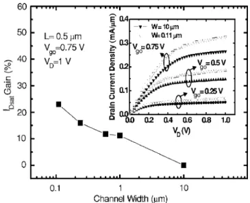
The device under test was an n-channel MOSFET fabri-cated using the concept of process tensile strain, mainly through the trench isolation.6The physical gate oxide thick-ness was 1.4 nm as determined by capacitance-voltage fit-ting. The channel length was 0.5m while the channel width spanned a wide range of 0.11, 0.24, 0.6, 1, and 10m. Here, a reduction in channel width means an enhancement in tensile strain in the channel width direction. This can be easily understood by means of the current drive enhancement factor against channel width as shown in Fig. 1. The inset of the figure displays measured drain current per unit channel width versus drain voltage with the gate overdrive as a pa-rameter. As expected, the drain current per unit channel width increases as the channel width is decreased. The
in-creased drain current can be well related to the mobility en-hancement; that is, the tensile stress causes subbands energy shift, which in turn suppresses the intervalley phonon scat-tering while reducing the effective conductivity mass, thereby enhances the mobility.1,7
The low-frequency noise measurement setup used was the same as that detailed elsewhere.4The measurement fre-quency ranged from 3 Hz to 100 kHz while operating the devices at a drain voltage of 0.2 V. Here, the noise experi-ment was carried out in terms of the input-referred noise voltage spectral density SVg. Figure 2 depicts measured SVg
versus frequency for a gate overdrive of 0.6 V, where three devices, as labeled A, B, and C with the same channel width
a兲Electronic mail: [email protected]
FIG. 1. The experimental drain current enhancement factor vs channel width for gate overdrive Vgo= 0.75 V and drain voltage VD= 1 V. The inset shows measured drain current per unit channel width vs drain voltage with gate overdrive as a parameter.
APPLIED PHYSICS LETTERS 88, 063511共2006兲
0003-6951/2006/88共6兲/063511/3/$23.00 88, 063511-1 © 2006 American Institute of Physics
This article is copyrighted as indicated in the article. Reuse of AIP content is subject to the terms at: http://scitation.aip.org/termsconditions. Downloaded to IP: 140.113.38.11 On: Thu, 01 May 2014 02:08:31
of 0.11m, represent three different positions on the wafer. Apparently, a considerable variation of low-frequency noise exists between devices, which can be attributed to statistical fluctuations of the number of the interface traps.8Hence, it is argued that the measured noise data essentially can follow the 1 / f␥ relationship with the power coefficient ␥ close to unity.
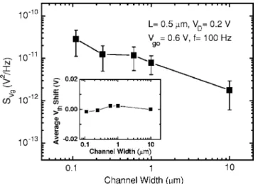
Figure 3 shows measured SVgagainst channel width for a
certain gate overdrive of 0.6 V at a specific frequency of 100 Hz. In this figure, each of the five error bars represents the standard deviation of the distribution created from a total of fifteen samples; and the data point stands for the mean of the distribution. This figure reveals that the low-frequency noise, on the average, increases with decreasing channel width. We also further conducted the case of varying gate overdrive and found that no significant deviation from that in Fig. 3 can be observed, provided that the gate overdrive of more than 0.4 V is applied.
Also shown in Fig. 3 is the corresponding average threshold voltage shift with respect to the wide structure共i.e., 10m兲 such as to address the possibility of the inverse nar-row width effect共INWE兲 caused by the impurity segregation
and the fringing electric field at the isolation sidewall.9,10 It can be seen that the threshold voltage shift is rather small共 ⬍5%兲, indicating that the inverse narrow width effect is not a significant issue in the undertaken devices. Furthermore, since the noise data are obtained in strong inversion, the channel current part along the edge of the channel is not significant relative to the overall channel one. As a result, the inverse narrow width effect can be substantially weakened. Therefore, it is reasonably drawn that the present low-frequency noise is a good tool to monitor the Si-SiO2 inter-face over the whole channel area.
The weak dependence of low-frequency noise on gate overdrive 共⬎0.4 V兲 as mentioned above suggests that the carrier number fluctuations prevail in the strong inversion mode. In other words, under such situations the Coulomb scattering can be ignored due to the screening of the trapped charge by the gate electrode and the inversion-layer charge. Hence, the following input-referred noise voltage spectral density expression can be adequately cited3,11
SVg= q2kBT Ceff2 Nt WL 1 f␥, 共1兲
where q is the elementary charge, kBis Boltzman’s constant,
T is the absolute temperature, is the tunneling distance
共⬃0.1 nm兲, W is the channel width, L is the channel length,
Ceffis the effective gate oxide capacitance per unit area, and
Nt is the effective near-interface oxide trap density. With
known Ceff共⬇1.75F / cm2兲 from the undertaken
manufac-turing process, fitting of all the SVgdata using Eq.共1兲 led to
the distribution of Nt as shown in Fig. 4 versus channel
width. Again on the average, the interface state density de-creases with decreasing channel width. Specifically, a reduc-tion in channel width by a factor of about 100 produces a tenfold reduction in interface state density. Once again, a reduction in channel width means an enhancement of tensile strain in that direction; therefore, the present noise experi-ment points to a reduction in interface state density in the presence of enhanced tensile strain in the channel width direction.
It is interesting to further examine the physical origin of the underlying interface states. Analogous to the electron-spin resonance 共ESR兲 experiment on a 共111兲 Si-SiO2
interface,12–14 the interface states investigated in our low-frequency noise work can be attributed to the group of Pb
centers共or equivalently the dangling-bond defects as charac-terized in terms of Si3⬅Si.兲 caused by the lattice mismatch FIG. 2. The measured input-referred noise voltage spectral density at Vgo
= 0.6 V and VD= 0.2 V vs frequency for three different positions on the wafer.
FIG. 3. The measured input-referred noise voltage spectral density at a specific frequency of 100 Hz vs channel width for Vgo= 0.6 V and VD = 0.2 V. The error bar represents the standard deviation of the distribution and the data point the mean of the distribution. The inset shows the corre-sponding average threshold voltage Vthshift with the wide structure共i.e., 10m兲 as a reference point. Here, the threshold voltage was determined at
VD= 0.025 V.
FIG. 4. The extracted effective interface state density corresponding to Fig. 3.
063511-2 Lu, Lee, and Chen Appl. Phys. Lett. 88, 063511共2006兲
This article is copyrighted as indicated in the article. Reuse of AIP content is subject to the terms at: http://scitation.aip.org/termsconditions. Downloaded to IP: 140.113.38.11 On: Thu, 01 May 2014 02:08:31
at the 共100兲 Si-SiO2 interface. Here, the lattice-mismatch
stress is primarily related to the thermal oxidation process since in this process about 2.2 unit volumes of oxide are produced for each unit volume of silicon consumption. Ob-viously, the lattice mismatch can be reduced using a tensile strain, thereby leading to a reduction in Pb centers.14 Note
that there were few studies on the usage of the ESR tech-nique to detect Pbcenters in the case of共100兲 Si-SiO2
inter-face. The noise experiment on the共100兲 Si-SiO2interface in this work again corroborates the action of applying a tensile strain: Enlarging the Si-Si interatomic distance before the
silicon oxidation process is carried out, which leads to re-duced lattice-mismatch stress during the subsequent thermal oxidation process.
Channel-width-dependent low-frequency noise measure-ment has been applied on a process tensile strained n-channel MOSFET. One important finding has been straightforwardly created: Enhanced tensile strain in the channel narrowing
direction can reduce the lattice-mismatch defects.
This work was supported by the National Science Coun-cil of Taiwan under Contract No. NSC 93-2215-E-009-002.
1S. E. Thompson, M. Armstrong, C. Auth, M. Alavi, M. Buehler, R. Chau, S. Cea, T. Ghani, G. Glass, T. Hoffman, C. H. Jan, C. Kenyon, J. Klaus, K.
Kuhn, Z. Ma, B. Mcintyre, K. Mistry, A. Murthy, B. Obradovic, R. Nagisetty, P. Nguyen, S. Sivakumar, R. Shaheed, L. Shifren, B. Tufts, S. Tyagi, M. Bohr, and Y. El-Mansy, IEEE Trans. Electron Devices 51, 1790 共2004兲.
2M. J. Kirton and M. J. Uren, Adv. Phys. 38, 367共1989兲.
3K. K. Hung, P. K. Ko, C. Hu, and Y. C. Cheng, IEEE Trans. Electron Devices 37, 654共1990兲.
4M. J. Chen, T. K. Kang, Y. H. Lee, C. H. Liu, Y. J. Chang, and K. Y. Fu, J. Appl. Phys. 89, 648共2001兲.
5E. Simoen, G. Eneman, P. Verheyen, R. Delhougne, R. Loo, K. De Meyer, and C. Claeys, Appl. Phys. Lett. 86, 223509共2005兲.
6C. H. Ge, C. C. Lin, C. H. Ko, C. C. Huang, Y. C. Huang, B. W. Chen, B. C. Perng, C. C. Sheu, P. Y. Tsai, L. G. Yao, C. L. Wu, T. L. Lee, C. J. Chen, C. T. Wang, S. C. Lin, Y. C. Yeo, and C. Hu, Tech. Dig. - Int. Electron Devices Meet. 73共2003兲.
7S. Takagi, J. L. Hoyt, J. J. Welser, and J. F. Gibbons, J. Appl. Phys. 80, 1567共1996兲.
8M. J. Uren, D. J. Day, and M. J. Kirton, Appl. Phys. Lett. 47, 1195 共1985兲.
9M. Sugino and L. A. Akers, IEEE Electron Device Lett. 4, 114共1983兲. 10S. K. H. Fung, M. Chen, and P. K. Ko, Solid-State Electron. 41, 1885
共1997兲.
11H. M. Bu, Y. Shi, X. L. Yuan, J. Wu, S. L. Gu, Y. D. Zheng, H. Majima, H. Ishikuro, and T. Hiramoto, Appl. Phys. Lett. 76, 3259共2000兲. 12E. H. Poindexter, P. J. Caplan, B. E. Deal, and R. R. Razouk, J. Appl.
Phys. 52, 879共1981兲.
13A. Stesmans, Phys. Rev. B 48, 2418共1993兲.
14A. Stesmans, D. Pierreux, R. J. Jaccodine, M. T. Lin, and T. J. Delph, Appl. Phys. Lett. 82, 3038共2003兲.
063511-3 Lu, Lee, and Chen Appl. Phys. Lett. 88, 063511共2006兲
This article is copyrighted as indicated in the article. Reuse of AIP content is subject to the terms at: http://scitation.aip.org/termsconditions. Downloaded to IP: 140.113.38.11 On: Thu, 01 May 2014 02:08:31