國
立
交
通
大
學
電子工程學系 電子研究所碩士班
碩
士
論
文
區別製程邊界來提高記憶體編譯器產生出來的
靜態隨機記憶體良率
On Distinguishing Process Corner for Yield Improvement in
Memory Compiler Generated SRAM
研 究 生:蕭家棋
指導教授:陳宏明 博士
區別製程邊界來提高記憶體編譯器產生出來的
靜態隨機記憶體良率
On Distinguishing Process Corner for Yield Improvement in
Memory Compiler Generated SRAM
研 究 生:蕭家棋 Student:Chia-Chi Hsiao
指導教授:陳宏明 博士 Advisor:Dr. Hung-Ming Chen
國 立 交 通 大 學
電子工程學系 電子研究所碩士班
碩 士 論 文
A Thesis
Submitted to Department of Electronics Engineering & Institute of Electronics College of Electrical and Computer Engineering
National Chiao Tung University in partial Fulfillment of the Requirements
for the Degree of Master
in
Electronics Engineering October 2008
Hsinchu, Taiwan, Republic of China
區別製程邊界來提高記憶體編譯器產生出來的靜態隨機記憶體良率
學生:蕭家棋 指導教授:陳宏明 博士 國立交通大學 電子工程學系 電子研究所 碩士班 摘 要 當製程持續的縮小至奈米等級時,因為晶粒與晶粒間的變異,將使得良率降低的 情況越來越嚴重,而使用適當的基版偏壓技術可以有效的減小這個問題。然而要 運用這一項技術我們必須先知道一個晶粒是屬於高臨界電壓或是低臨界電壓(也 稱之為製程邊界)。但是很不幸地,當 PMOS 與 NMOS 的變異是沒有關聯時我們將 很難偵測出他們的製程邊界。在這篇論文中,我們針對延遲監視器與漏電流監視 器這兩種電路做了一些改善,使得當 PMOS 與 NMOS 變異為不相關時也能分別偵測 出他們的製程邊界。由實驗結果我們可以看出我們的電路可以清楚的區別製程邊 界,因此可以順利的採用正確的基板電壓來提升良率。On Distinguishing Process Corner for Yield Improvement in Memory
Compiler Generated SRAM
Student: Chia-chi Hsiao Advisor: Prof. Hung-Ming Chen
Department of Electronics Engineering Institute of Electronics
National Chiao Tung University ABSTRACT
As the technology scales down to nanometer, the yield degradation caused by inter-die variations is getting worse. Using adaptive body bias is an effective method to eliminate the yield degradation, however we need to know a die having high threshold voltage or low threshold voltage (also called process corner) in order to use this technique. Unfortunately, it is hard to detect the process corner when PMOS and NMOS variations are uncorrelated. In this thesis, we propose some improved circuits of delay monitor and leakage monitor for both PMOS and NMOS having inter-die variations, and are uncorrelated. The experimental results show that our circuits can clearly distinguish each process corner of PMOS and NMOS, thus improve the yield obviously by adopting correct body bias.
誌 謝
這篇論文能夠完成,需要感謝很多人。首先要感謝的是我的指導教授陳宏明 博士。陳教授在我兩年的碩士生涯裡,在我課業上細心的指導;在我論文的研究 上,給予我相當多的寶貴意見與可行的方向,讓我能夠順利的完成畢業論文;另 外教授也相當關心我的生活,這兩年在老師的實驗室中感到相當的溫馨。 再來我要感謝莊景德教授與張孟凡教授。他們兩位教授在我口試期間給予我 很多關於記憶體方面的知識以及我論文中的缺失,讓我能把論文做正確的修正。 我要感謝實驗室的佳毅學長,平時學長教了我很多工作站上的東西,而在最 後撰寫論文的期間,學長也幫我匡正了很多我論文中錯誤的部分。 感謝仁傑學長,在我就讀研究所期間給予我很多課業上的幫助。 感謝黃柏蒼學長在我還在摸索記憶體的階段給予我很多記憶體方面的知識。 感謝鍾菁哲博士讓我在軟體取得與使用上能夠很順利。 感謝實驗室的同學智偉、柏州、昆生、篤雄、睿斌、芳瑜。在這段期間與我 一同學習,並給予我鼓勵與幫助。 最後我要感謝我的家人,在我就讀研究所期間給予我的鼓勵與支持。 蕭家棋 民國九十七年十月 於新竹Contents
1 Introduction 1
1.1 Our Contribution . . . 2
1.2 Thesis Organization . . . 3
2 Preliminary 4 2.1 Process Variations and Yield . . . 4
2.2 Previous Works . . . 5
2.2.1 Adaptive Body Bias . . . 6
2.2.2 Leakage Monitor . . . 6
2.2.3 Delay Monitor . . . 7
2.3 Problem Description . . . 8
3 Improved Circuits for PMOS and NMOS Variations 9 3.1 Delay Monitor for PMOS and NMOS Variations . . . 9
3.1.1 PMOS Variations Detector Using Delay Monitor . . . 12
3.1.2 NMOS Variations Detector Using Delay Monitor . . . 16
3.1.3 Modified Circuits for NMOS Variations . . . 16
3.2.1 Inverter Array . . . . 20
3.2.2 PMOS Variations Detector Using Leakage Monitor . . . 20
3.2.3 NMOS Variations Detector Using Leakage Monitor . . . 23
3.3 Discussion . . . 25
4 Experimental Results 26
4.1 Single Port SRAM . . . 26
4.2 Dual Port SRAM . . . 29
5 Conclusions 34
List of Figures
2.1 Effect of intra-die and inter-die variations. (a) A chip only suffers from intra-die variations. (b) A chip suffers from both intra-die and
inter-die variations. . . 5
2.2 The leakage monitor approach to detecting inter-die variations [1]. . 7
2.3 The delay monitor approach to detecting inter-die variations [1]. . . 8
3.1 The result of 1000 iteration of Monte-Carlo analysis of 300 stages inverter chain. The delay time is almost located between 6.4ns and
6.6ns. . . 14
3.2 Modified circuit block diagram for detecting NMOS variations. This circuit can eliminate the effect of PMOS variations when detecting
the process corner of NMOS. . . 19
3.3 We replace the active NMOS loading with cascade three NMOS
de-vices when detecting PMOS variations. . . 21
3.4 We apply body bias to the two PMOS driver when detecting the
List of Tables
3.1 The delay time and required clock cycles at different inter-die vari-ations using the circuit in [1]. The numerical values in columns 3 to 5 express the real delay time of a signal passing through the long inverter chain, and the numerical values in the last 3 columns express
the real delay time transferred to required clock numbers. . . 10
3.2 Our improved circuits using zero and adaptive body bias at detecting
stage. . . 13
3.3 The results of detect PMOS inter-die variations. In this table we can see that each kind of PMOS variations(HVT NVT and LVT) are
separated. . . 15
3.4 The results of detecting NMOS variations. In this table we can see that the delay time are affected by PMOS variations hence we can
not separate each kind of NMOS variations. . . 17
3.5 The results of modified circuits to detect NMOS variations. In this table we can see that the effect of PMOS variations have been
re-moved. . . 18
3.6 The results of using traditional active load to detect the process corner of PMOS. The numerical values in the last 3 columns express the
3.7 The results of modified circuits detect PMOS variations. The high threshold process corner of PMOS can set at 0.3v and the low corner
can set at 0.45v. Each kind of PMOS variations are separated. . . 22
3.8 The results of our circuits to detect NMOS variations. Each kind of
NMOS variations are separated. . . 24
4.1 Total failure number of the single port SRAM with 125mv assumption for inter-die variations and 75mv assumption for intra-die variations. In this table we can see that our circuits can always improve the yield. The ‘0’ and ‘1’ in second row represent the action of ‘write 0 then read the data out’ and ‘write 1 then read it out’ respectively. The numerical values in row 3 to row10 express the failure numbers
in 640times test. . . 27
4.2 Total failure number of the single port SRAM with 150mv assumption for inter-die variations and 75mv assumption for intra-die variations. In this table we can see that when PMOS and NMOS both have high threshold the yield degrades very much, and using only NMOS body
bias can not satisfy the requirement of yield improvement. . . 28
4.3 Total failure number of the single port SRAM with 175mv assumption for inter-die variations and 75mv assumption for intra-die variations. In this table we can see that even we get the wrong predictions, our yield are still very close to the right prediction of only use NMOS
body bias. . . 29
4.4 Total failure number of the single port SRAM with 200mv assumption for inter-die variations and 75mv assumption for intra-die variations. In this table we can see that using body bias can not improve much
4.5 Total failure number of the dual port SRAM with 125mv assumption for inter-die variations and 75mv assumption for intra-die variations. In this table we can see that when both PMOS and NMOS have high threshold voltage, we get the results of 640 failures in read 1. This
means that the failure probability is 100% . . . 31
4.6 Total failure number of the dual port SRAM with 150mv assumption for inter-die variations and 75mv assumption for intra-die variations. In this table we can see that our circuits can not solve the all failure
happened when both PMOS and NMOS having high threshold voltage. 31
4.7 Total failure number of the dual port SRAM with 175mv assumption for inter-die variations and 75mv assumption for intra-die variations. In this table we can see that our circuits can improve the yield much better than using only NMOS body bias, especially for PMOS having
high threshold voltage and NMOS having normal threshold voltage. . 32
4.8 Total failure number of the dual port SRAM with 200mv assumption for inter-die variations and 75mv assumption for intra-die variations. In this table we can see that there is another all failure happened at the case of PMOS having high threshold and NMOS having normal threshold. In this case, using only NMOS body bias can not improve the yield, but using both PMOS and NMOS body bias can have
Chapter 1
Introduction
With reduction in technology feature sizes, the MOS size becomes very small. The threshold voltage variations caused by random dopant fluctuation (RDF) is inversely proportional to gate area [2] [3] [4], thereby the probability of device mismatch increases greatly. This is especially obvious to SRAM. Because SRAM cell always uses the smallest manufacture devices size [5] to ensure having high density, SRAM faces with more challenges about process variations than normal digital circuits.
In recent years, process variation becomes a very important issue. As the tech-nique scales down to nanometer, the device parameters, such as gate length and oxide thickness, suffer from significant variations. Typically process variations are classified as systematic and random. Systematic variations are predictable and usu-ally depend on layout structure [6] [7]. On the other hand, random variations are unpredictable and usually caused by fabrication process such as the number and lo-cation of dopant atoms in channel region [8]. In each kind of process variations, the threshold voltage mismatch is one of the most important issues. The authors in [1] concern the case which NMOS and PMOS variations are correlated. The situation happens when PMOS and NMOS variations are uncorrelated, it is hard to detect the process corner. The reason is that when detecting the process corner of PMOS, the results will be interfered from NMOS variations, which makes the detection fail.
Hence we need an improved circuit to be able to detect PMOS and NMOS variations individually. If we do not consider the process variations in design stage, the real yield of the design will be far away from our expectation.
Memory is commonly used in various kinds of ICs. When designers design a digital circuit, memory compiler is a popular tool to provide the designers SRAM so as to integrate memory circuit with their digital circuits. In order to guarantee good yield, a memory compiler should be able to provide the components with the tolerance to high process variations. In this thesis, our purpose is to make the circuits generated from memory compiler better and immune from process variations.
1.1
Our Contribution
In this thesis, we use the SRAM circuits from memory compiler as our test circuits. Our main contributions are as follows:
• We propose some improved circuits for delay monitor and leakage monitor to
detect both PMOS and NMOS variations. Based on the detection results, we apply global body bias to both PMOS and NMOS. The goal is to mitigate the read-write fail caused by the inter-die variations.
• In order to have more complete analysis, we not only use single port SRAM
but also use dual port SRAM as test circuits. In some cases PMOS variations have more influence on the predictive yield than NMOS variations, hence both NMOS and PMOS detect circuits are more effective to improve yield.
• The experimental results show that our yield improvement is much better than
the improvement using only NMOS body bias in some variations situations, and our circuits can guarantee that we always apply correct PMOS body bias.
1.2
Thesis Organization
This thesis is organized as follows. In Chapter 2, we discuss how process variations decrease the yield and review some previous works about how to decrease the effect of inter-die variations. In Chapter 3, we discuss our improved circuits, and Chapter 4 shows the experimental results. Finally, we conclude our work in Chapter 5.
Chapter 2
Preliminary
In this chapter, we discuss how process variations decrease the yield and introduce previous works in using adaptive body bias to decrease the effect of process varia-tions.
2.1
Process Variations and Yield
As the technique scales down to nanometer, inter-die variations and intra-die vari-ations cause parametric failures and yield degradation. The intra-die varivari-ations mean that the devices existing on a same die but having different location may have different device features. The inter-die variations mean that the devices exist-ing on different dies may have different device features [9]. Generally speakexist-ing, the intra-die variations are the primary reasons for parametric failures, and the inter-die variations make the problem more serious. To explain this phenomenon, we can see Figure 2.1. Figure 2.1a shows that a chip suffers from intra-die variations. Some dies locate out of the spec (the shadow regions) and cause functional failure. Figure 2.1b shows that a chip suffers from intra-die variations and has inter-die variations at the same time. The inter-die variations make the curve shift right. Obviously, we can see the failure number is much more than the number of intra-die variations. To improve the yield, eliminating intra-die variations should be the most effective
way. Unfortunately, to solve the intra-die variations is very difficult, so a feasible method is to decrease the inter-die variations.
Delay time # o f o cc u ra n ce Out of spec Delay time # o f o cc u ra n ce Out of spec
(a) intra-die variations (b) intra-die plus inter-die variations
Figure 2.1: Effect of intra-die and inter-die variations. (a) A chip only suffers from intra-die variations. (b) A chip suffers from both intra-die and inter-die variations.
2.2
Previous Works
In order to decrease the effect of process variations in SRAM architectures, many methods have been proposed. Some new SRAM cell architectures are presented [10] [11] [12]. Moreover, typical 6-T SRAM cell architecture use additional circuits to enhance the yield, such as using adaptive body bias [13] [1] [14]. Because the memory compiler use typical 6-T SRAM cell, hence we focus on adaptive body bias. By the results of [13] we can see that adaptive body bias is an effective method to improve SRAM yield. In order to use the technique we need some circuits to detect the process corner. In [13] [1] [14], the authors use leakage monitor and delay monitor to detect the dies having high threshold voltage or low threshold voltage. In [15] the authors propose a method using delay and slew-rate monitor to detect the process corner.
2.2.1
Adaptive Body Bias
In Section 2.1, we have known that different devices in different die may have dif-ferent parametric features due to inter-die variations. This difdif-ferent device feature may cause that one die has good yield but another die has poor yield, hence it is necessary to eliminate the inter-die variations. Some works use adaptive body bias to make different die having smaller threshold voltage difference [16]. The principle is that when we know that a die belongs to high threshold voltage, we can provide this die forward body bias to decrease the threshold voltage. Similarly, when we know that a die belongs to low threshold voltage, we can provide this die reverse body bias to increase the threshold voltage. Using this technique we can make every die tend to have normal threshold voltage, and improve the yield. This method is used to improve the yield of logic design [16]. The authors of [13] use this method to improve SRAM yield for the first time.
2.2.2
Leakage Monitor
Here we describe the principle of leakage monitor. In Figure 2.2 we can see the authors use a current sensor circuit to monitor the leakage of SRAM array and generate a voltage to comparator. This generated output voltage is proportional to the SRAM leakage value. When the SRAM array has high threshold voltage, the leakage will be very small and the generated output signal will have high voltage. On the other hand, when the SRAM array has low threshold voltage, the leakage of SRAM array will be large and the generated output signal will have low voltage. Next, the comparator circuits compare the monitor output voltage with two refer-ence voltages. These two referrefer-ence voltages represent a die at high threshold corner and low threshold corner respectively. According to this result, we can make sure that this die belongs to high or low threshold, and the body bias selection circuit will apply correct body bias to the SRAM array. Besides, to avoid performance loss
due to the voltage drop across the leakage monitor, a large PMOS switch bypasses the leakage monitor at normal mode operates.
Figure 2.2: The leakage monitor approach to detecting inter-die variations [1].
2.2.3
Delay Monitor
Another way to know a die with high or low threshold voltage is using delay monitor[1] [14]. Figure 2.3 shows the delay monitor circuits. It is composed of a 600 stages long inverter chain, a counter circuit, and the comparator circuits. We introduce the principles of delay monitor as follows. First, a calibrate signal passes through the long inverter chain and enables the counter at the same time. If one die has high threshold voltage, the delay time of the calibrate signal passing through the long inverter chain will be very large. On the other hand, if one die has low threshold voltage, the delay time will be very short. Second, the counter is disabled at the rising edge of the signal from the output of inverter chain. The counter cir-cuit is used to count the total delay time of the long inverter chain. Finally, the comparator circuits are used to compare with two references which are represented
will apply the right body bias to SRAM array according to the result of comparator. counter State comparator State comparator REF1 REF2 Body bias selection Calibrate CLK
Long inverter chain
Enable Disable CLK
Body bias voltage
Figure 2.3: The delay monitor approach to detecting inter-die variations [1].
2.3
Problem Description
Based on the previous discussion we know that the adaptive body bias is a powerful way to decrease the yield degradation generated by inter-die variations. In real manufacturing flow, the lithography parameters cause the PMOS and NMOS having correlated inter-die shift. It means that both PMOS and NMOS move to high or low threshold voltage. Other sources, such as global variations in p-type and n-type doping density, can result in non-correlated threshold voltage shift for PMOS and NMOS [14]. So it is necessary to detect the process corner of PMOS and NMOS variations individually. Since previous works ([13] [1] [14]) assumed that PMOS and NMOS variations are correlated, which is not complete correct, we try to develop different circuits to detect the variations of PMOS and NMOS individually.
Chapter 3
Improved Circuits for PMOS and
NMOS Variations
In this chapter we first present the results of using the circuits in [14] to detect the process corner when PMOS and NMOS variations are uncorrelated. And then discuss our proposed circuits of leakage monitor and delay monitor to further distin-guish those variations individually. We apply NMOS body bias, hence our circuits must use triple-well process.
3.1
Delay Monitor for PMOS and NMOS
Varia-tions
Table 3.1 shows the variations results of the circuits discussed in [1], but the PMOS and NMOS variations are not always correlated. We assume that the die suffers from both inter-die and intra-die variations: the intra-die variations have 75mv at 3-sigma and the distribution is random (based on [17]), the inter-die variations are
given from 125mv to 200mv, which are referred to [1] and [14]. 1
In Table 3.1, the first column shows the inter-die variations of PMOS and NMOS. For instance, the first row 125-125 means PMOS suffer from 125mv
inter-1In these two papers, the authors use 70nm process and set the variations corner at 100mv, and
Table 3.1: The delay time and required clock cycles at different inter-die variations using the circuit in [1]. The numerical values in columns 3 to 5 express the real delay time of a signal passing through the long inverter chain, and the numerical values in the last 3 columns express the real delay time transferred to required clock numbers. 125-125 PMOS NMOS HVT NVT LVT PMOS NMOS HVT NVT LVT HVT 13.1 10.73 9.309 HVT 15 13 F11 NVT 11.12 9.044 7.813 NVT ♠13 11 ♦9 LVT 9.597 7.891 6.795 LVT F11 9 8 150-150 PMOS NMOS HVT NVT LVT PMOS NMOS HVT NVT LVT HVT 14.28 11.18 9.457 HVT 17 13 F11 NVT 11.71 9.044 7.626 NVT 14 11 ♦9 LVT 10 7.714 6.462 LVT F12 9 8 175-175 PMOS NMOS HVT NVT LVT PMOS NMOS HVT NVT LVT HVT 15.69 11.71 9.665 HVT 18 14 F11 NVT 12.35 9.044 7.461 NVT ♠15 11 ♦9 LVT 10.36 7.542 6.186 LVT F12 9 8 200-200 PMOS NMOS HVT NVT LVT PMOS NMOS HVT NVT LVT HVT 17.28 12.3 9.923 HVT 20 14 F12 NVT 13.1 9.044 7.298 NVT ♠15 11 ♦9 LVT 10.54 7.405 5.933 LVT F12 9 7
die and NMOS suffer from 125mv inter-die. This 125mv inter-die voltage is added to normal threshold voltage hence the values of PMOS threshold voltage are from (NVT-125) mv in LVT to (NVT+125) mv in HVT. Other columns with HVT, NVT, LVT represent high threshold voltage, normal threshold voltage, and low threshold voltage respectively. The numerical values in columns 3 to 5 express the real delay time of a signal passing through the long inverter chain, and the numerical values in the last 3 columns express the real delay time transferred to needed clock numbers. For example, the value 10.54 in the last row and column 3 means PMOS has high threshold voltage (200mv higher than normal threshold) and NMOS has low threshold voltage (200mv lower than normal value). The calibrate signal passes through the long inverter chain needs 10.54ns. This value of delay needs 12 clock cycles. (Here the clock period is 0.88ns, which is the minimal clock period of our SRAM array.) In order to show the data more clearly, we just list the required cycle values for the following tables.
Based on [1], we may set the high threshold corner at 13 cycles and the low threshold corner at 10 cycles. We observe that when PMOS has high threshold voltage and NMOS has low threshold voltage (or PMOS has low threshold voltage and NMOS has high threshold voltage), the traditional delay monitor will be under the impression that this die has normal threshold voltage and suggest the NMOS zero body bias. The traditional circuits do not revise the body bias of PMOS, and this will cause the problem. We indicate this situation with symbol F in Table 3.1. Another error will happen when PMOS has high threshold voltage and NMOS has normal threshold voltage. In this case, the circuits will be under the impression that the NMOS has high threshold voltage and suggest NMOS forward body bias, in result we get the wrong body bias. This situation is indicated with symbol ♠. The last kind of error happens when PMOS has low threshold voltage and NMOS has normal threshold voltage. In this case the circuits will be under the impression
that the NMOS has low threshold voltage and suggest the reverse body bias. We indicate this situation with symbol ♦.
Based on the previous discussion, we know that if we do not concern the PMOS variations, using delay monitor may make a mistake and the probability of making this mistake is nearly 50%. Moreover, it may cause the yield worse than without using body bias in some cases. Therefore, it is necessary to concern the effect of both PMOS and NMOS variations.
3.1.1
PMOS Variations Detector Using Delay Monitor
By observing Table 3.1, we can see that if we know the process corner of PMOS, then we can detect the process corner of NMOS successfully. For example, if we know that PMOS has high threshold voltage, the delay at 125mv assumption for inter-die variations will be 11 or 13 or 15 cycles. These three kinds of values are divided away hence we can distinguish each other and know the NMOS variations. If we do not know the process corner of PMOS variations, we can not know NMOS variations if the delay is 11 cycles. This is because that delay of 11 cycles may happen at PMOS having high threshold voltage and NMOS having low threshold voltage; or PMOS having low threshold voltage and NMOS having high threshold voltage. Due to those two cases, we do not know which one contributes 11 cycles delay time. Similarly, if we know the process corner of NMOS first, we can distinguish the PMOS variations as well. Therefore the problem becomes to know the process corner of the first type MOS variations. Our approach is presented in the following subsections.
According to the previous discussion we know that if we want to detect the process corner of PMOS, we must remove the effect of NMOS variations. In order to achieve this, we let the PMOS and NMOS mismatch, that is, the size of PMOS are 100nm/90nm and NMOS are 110nm/90nm. Here we let PMOS have less driver ability. The delay will be dominated by PMOS thus degrading the effect of NMOS.
We do not use 1V supply voltage, but use 0.7V in order to increase the difference between PMOS and NMOS driver ability. Furthermore, we do not use the normal body bias, but apply forward body bias to NMOS, and apply reverse body bias to PMOS of detect circuit at detecting stage.
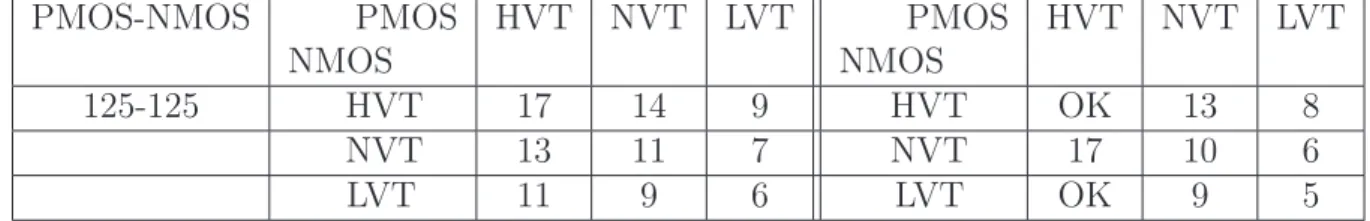
In Table 3.2, column 2 to column 5 represent the situation that we use zero body bias and column 6 to column 9 represent the situation that we use adaptive body bias on detecting circuits. We can see that using correct body bias on detecting circuits can separate each kind of PMOS variations (HVT, NVT or LVT), which means we can detect PMOS variations successfully. For example, the minimal required cycles of PMOS having high threshold voltage is 17 cycles, and the maximal require cycles of PMOS having normal threshold voltage is 13 cycles. Therefore, we can distinguish high threshold voltage from normal threshold voltage. The same situation applies for the normal threshold voltage and low threshold voltage. Here “OK” in Table 3.2 and following tables means the required cycle number is larger than 24.
Table 3.2: Our improved circuits using zero and adaptive body bias at detecting stage. PMOS-NMOS PMOS NMOS HVT NVT LVT PMOS NMOS HVT NVT LVT 125-125 HVT 17 14 9 HVT OK 13 8 NVT 13 11 7 NVT 17 10 6 LVT 11 9 6 LVT OK 9 5
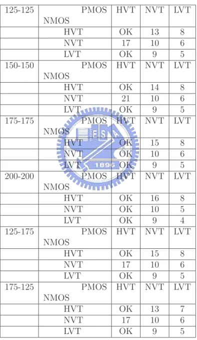
Table 3.3 shows the results when we use our circuits to detect PMOS inter-die variations. We set the PMOS high threshold corner at 17 and low threshold corner at 8. The results show that we can separate each kind of PMOS variations. There is a worse case when PMOS variations are small and NMOS variations are large. If PMOS variations are small, it will make the circuits difficult to detect the process corner of PMOS, similarly when NMOS variations are large, the effect of
NMOS variations will hard to be removed. We can separate each kind of PMOS variations by using proposed circuits when PMOS having 125mv assumption for inter-die variations and NMOS having 175mv assumption for inter-die variations.
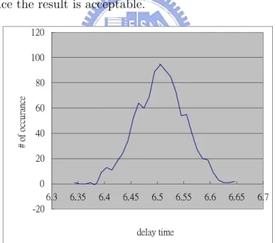
It is worth mentioning that we only use 300 stages inverter in the long inverter chain, while the circuits in [1] use 600 stages inverter. The reason shows as follows. The purpose of using long inverter chain is that we want to eliminate the effect of intra-die variations. According to our experimental results we can see that using only 300 stages can achieve this. We run 1000 times Monte-Carlo to test our 300 stages inverter chain. Figure 3.1 shows the result of test. In this test we set each MOS having 75mv assumption for intra-die variations. The result shows that the delay time is almost located between 6.4ns and 6.6ns. It is much smaller than our clock period hence the result is acceptable.
Figure 3.1: The result of 1000 iteration of Monte-Carlo analysis of 300 stages inverter chain. The delay time is almost located between 6.4ns and 6.6ns.
Table 3.3: The results of detect PMOS inter-die variations. In this table we can see that each kind of PMOS variations(HVT NVT and LVT) are separated.
125-125 PMOS NMOS HVT NVT LVT HVT OK 13 8 NVT 17 10 6 LVT OK 9 5 150-150 PMOS NMOS HVT NVT LVT HVT OK 14 8 NVT 21 10 6 LVT OK 9 5 175-175 PMOS NMOS HVT NVT LVT HVT OK 15 8 NVT OK 10 6 LVT OK 9 5 200-200 PMOS NMOS HVT NVT LVT HVT OK 16 8 NVT OK 10 5 LVT OK 9 4 125-175 PMOS NMOS HVT NVT LVT HVT OK 15 8 NVT 17 10 6 LVT OK 9 5 175-125 PMOS NMOS HVT NVT LVT HVT OK 13 7 NVT 17 10 6 LVT OK 9 5
3.1.2
NMOS Variations Detector Using Delay Monitor
Now we have already detected PMOS variations, the next stage is to detect the process corner of NMOS. In this stage, we can not change the size of inverters since the inverter size has been determined in previous stage. In Section 3.1.2, we know that our MOS sizes are chosen for easily detecting PMOS variations. Here we want only NMOS variations to change delay time, we must correct the body bias of both PMOS and NMOS. We apply reverse body bias to NMOS and apply forward body bias to PMOS. The reverse body bias to NMOS makes NMOS delay time become larger and make the NMOS variations have more effect. The forward body bias to PMOS makes the signal pass through PMOS quickly and does not dominate the delay time. The result shows in Table 3.4. The result shows that our method has some effects but still not enough. The main problem is that the delay time is too short when PMOS has low threshold. In other words, PMOS variations still affect the delay time hence the detection of NMOS variations will fail. We need the following improved circuits to have better detections.
3.1.3
Modified Circuits for NMOS Variations
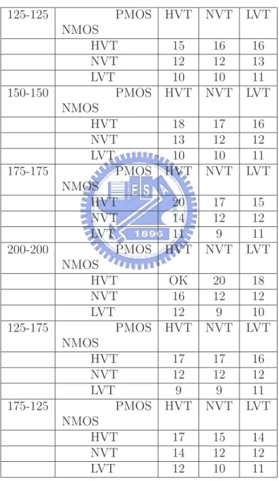
In Table 3.4 we can see that PMOS variations still affect the delay time. We do not separate each variation of NMOS, but we observe that if we change the initial value of counter (Figure 2.3) the results will be different. In order to accomplish this, we delay the enable signal of the counter circuit and show the block diagram in Figure 3.2.
If we have normal threshold PMOS, we let the enable signal delay 1 cycle to reach the counter circuit. If we have low threshold PMOS, we will delay 5 cycles. The modified results are shown in Table 3.5. Now we can know the process corner of NMOS by detecting the delay time. If the delay is more than 15 cycles, the NMOS
Table 3.4: The results of detecting NMOS variations. In this table we can see that the delay time are affected by PMOS variations hence we can not separate each kind of NMOS variations. 125-125 PMOS NMOS HVT NVT LVT HVT 15 15 11 NVT 12 11 8 LVT 10 9 6 150-150 PMOS NMOS HVT NVT LVT HVT 18 16 11 NVT 13 11 7 LVT 10 9 6 175-175 PMOS NMOS HVT NVT LVT HVT 20 16 10 NVT 14 11 7 LVT 11 8 5 200-200 PMOS NMOS HVT NVT LVT HVT OK 19 13 NVT 16 11 7 LVT 12 8 5 125-175 PMOS NMOS HVT NVT LVT HVT 17 16 11 NVT 12 11 7 LVT 9 8 6 175-125 PMOS NMOS HVT NVT LVT HVT 17 14 9 NVT 14 11 7 LVT 12 9 6
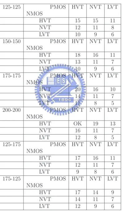
Table 3.5: The results of modified circuits to detect NMOS variations. In this table we can see that the effect of PMOS variations have been removed.
125-125 PMOS NMOS HVT NVT LVT HVT 15 16 16 NVT 12 12 13 LVT 10 10 11 150-150 PMOS NMOS HVT NVT LVT HVT 18 17 16 NVT 13 12 12 LVT 10 10 11 175-175 PMOS NMOS HVT NVT LVT HVT 20 17 15 NVT 14 12 12 LVT 11 9 11 200-200 PMOS NMOS HVT NVT LVT HVT OK 20 18 NVT 16 12 12 LVT 12 9 10 125-175 PMOS NMOS HVT NVT LVT HVT 17 17 16 NVT 12 12 12 LVT 9 9 11 175-125 PMOS NMOS HVT NVT LVT HVT 17 15 14 NVT 14 12 12 LVT 12 10 11
PMOS have high vt PMOS have normal vt
PMOS have low vt delay 5 cycles
delay 0 cycle
delay 1 cycle counter
enable signal
Figure 3.2: Modified circuit block diagram for detecting NMOS variations. This circuit can eliminate the effect of PMOS variations when detecting the process corner of NMOS.
belongs to high threshold NMOS. Similarly if the delay time is less than 11 cycles, the NMOS belongs to low threshold NMOS and others belong to normal threshold NMOS. In the worse case when PMOS has larger variations than NMOS, our circuits will have errors when PMOS with 175mv assumption for inter-die variations and NMOS with 125mv assumptions for inter-die variations. In the other situations, our circuits predict correctly.
In summary, our circuits have some difference with the traditional delay mon-itor. First, we make the inverter MOS mismatch to let the PMOS dominate the delay time. Second, we use different body bias at different stage and different sup-ply voltage to make the detection successfully. Third, we add a delay switch circuits to remove PMOS variations when NMOS variations are detected.
3.2
Leakage Monitor for PMOS and NMOS
Vari-ations
Similar to delay monitor, if we use traditional circuits to detect the variations with-out thinking PMOS variations, the errors will occur. The following subsections will present our modified leakage monitor circuits.
3.2.1
Inverter Array
Here we do some modification to the architecture Figure 2.2 for our usage. We replace leakage source from the SRAM array to an inverter array. The reasons are as follows. First, we use inverter array to be the test circuit, then bypass PMOS is no longer needed. Second, we can give a value we need but not limit on 0V or 1V to the input signal of inverter. We also change the loading circuits of current mirror since we want our modified circuits be able to detect NMOS and PMOS individually. Finally, we will add body bias on current mirror circuits when we detect NMOS variations. We set the inverter input at 0.7V. The reason is that we want the NMOS almost on and let PMOS almost off but having some leakage. According to experience we find that 0.7V is a better input signal value.
3.2.2
PMOS Variations Detector Using Leakage Monitor
Similar to delay monitor, we detect the PMOS variations first. Traditional current mirror results are shown in Table 3.6. We can see that NMOS variations influence the output, and the reason is the active NMOS loading. Hence the detection of PMOS variations fails. We modify the loading of the current mirror. The circuits are shown in Figure 3.3. We cascade three NMOS devices and connect their gate with a metal line to make them have the same gate voltage. The output is taken out by net1, and the result is shown in Table 3.7. We can see that cascade three NMOS removes the effect of active load NMOS variations.
In Table 3.7 the meaning of every element is the same as previous tables except the numerical values represent the output voltage. We set the high threshold corner at net1 having 0.3V and the low threshold corner at net1 having 0.45V. Here we only use the worse case to test our circuits. We can see that when we detect PMOS variations in the worst case (PMOS with 125mv assumption for inter-die variations
Table 3.6: The results of using traditional active load to detect the process corner of PMOS. The numerical values in the last 3 columns express the output voltage of current mirror. PMOS-NMOS PMOS NMOS HVT NVT LVT 125-125 HVT 0.5456 0.7190 0.8411 NVT 0.4399 0.5991 0.7126 LVT 0.3219 0.4793 0.5944
Figure 3.3: We replace the active NMOS loading with cascade three NMOS devices when detecting PMOS variations.
Table 3.7: The results of modified circuits detect PMOS variations. The high thresh-old process corner of PMOS can set at 0.3v and the low corner can set at 0.45v. Each kind of PMOS variations are separated.
125-125 PMOS NMOS HVT NVT LVT HVT 0.2107 0.426 0.532 NVT 0.2258 0.4196 0.5261 LVT 0.2177 0.4022 0.5126 125-200 PMOS NMOS HVT NVT LVT HVT 0.2215 0.4281 0.5352 NVT 0.2258 0.4196 0.5261 LVT 0.214 0.3933 0.5040 200-125 PMOS NMOS HVT NVT LVT HVT 0.1367 0.4265 0.5631 NVT 0.1458 0.4196 0.5586 LVT 0.1367 0.4022 0.5457 200-200 PMOS NMOS HVT NVT LVT HVT 0.1427 0.4381 0.5638 NVT 0.1458 0.4196 0.5586 LVT 0.1418 0.3933 0.5369
and NMOS with 200mv assumption for inter-die variations) we can still separate each kind of PMOS variations.
3.2.3
NMOS Variations Detector Using Leakage Monitor
In previous stage we have already known the process corner of PMOS, and we need to detect the NMOS variations. The circuits are similar to Figure 3.2. The difference is that we only use normal current mirror. In order to remove the influence of PMOS (two PMOS current mirror driver, MP1 and MP2), we give adaptive body bias to PMOS driver based on the results of first stage(Section 3.2.2). The circuits show in Figure 3.3, and the result is shown in Table 3.8. In Table 3.8, the meaning of every element is the same as Table 3.7. Here we also use the worse case to test our circuits. The result shows that even in the worst case (PMOS with 200mv assumption for inter-die variations and NMOS with 125mv assumption for inter-die variations) we can still separate each kind of NMOS variations.
Figure 3.4: We apply body bias to the two PMOS driver when detecting the process corner of NMOS.
Table 3.8: The results of our circuits to detect NMOS variations. Each kind of NMOS variations are separated.
125-125 PMOS NMOS HVT NVT LVT HVT 0.5336 0.4530 0.4820 NVT 0.4160 0.3316 0.36 LVT 0.2892 0.2154 0.2440 125-200 PMOS NMOS HVT NVT LVT HVT 0.6142 0.5314 0.5608 NVT 0.4160 0.3316 0.36 LVT 0.2303 0.1465 0.1752 200-125 PMOS NMOS HVT NVT LVT HVT 0.4916 0.4530 0.5271 NVT 0.3742 0.3316 0.4032 LVT 0.2576 0.2154 0.2865 200-200 PMOS NMOS HVT NVT LVT HVT 0.571 0.531 0.607 NVT 0.3742 0.3316 0.4032 LVT 0.1886 0.1465 0.2176
3.3
Discussion
When using our delay monitor circuits, the reason of detecting PMOS variations first is that its size is smaller than the circuit of detecting NMOS variations coming first. If we detect NMOS variations first, the NMOS variations must dominate the delay, in other words, the PMOS size must be much larger than NMOS. The required size may be PMOS with 400nm/90 and NMOS with 100nm/90nm to make PMOS have twice driving force to NMOS. The area is almost 2.5 times larger than the circuit which detecting PMOS variations first.
As for delay monitor issue, we know that our delay monitor circuits can separate each kind of variations clearly either PMOS or NMOS, but the drawback is the worse case. In worse case our circuits will confuse and may apply the wrong body bias to NMOS. However, detecting PMOS will not have this problem. So we can always aplly the correct PMOS body bias. On the other hand, our leakage monitor circuits can tolerate large variations but the drawback is we need a precise comparator.
Chapter 4
Experimental Results
We implement our circuits in HSPICE, and use memory compiler from FARADAY to build single port SRAM and dual port SRAM as our test circuits. We use the UMC 90nm CMOS library to implement our circuits.
4.1
Single Port SRAM
We use memory compiler to compile a 64-word (each word has 32 bits) single port SRAM. We use Monte-Carlo method to test the failure probability. We choose 640 cells per circuit as our test samples, and the result is shown in Table 4.1 to Table 4.4.
In Table 4.1, each test circuit suffers from both inter-die and intra-die variations. The value of inter-die variations is 125mv and the value of intra-die variations is
75mv. 1 The meaning of each element is as follows. The first column represents
the process corner of PMOS and NMOS respectively. For example, the first column and the bottom row represents PMOS has low threshold voltage and NMOS has
1We add the inter-die and intra-die variations to the MOS parameter ‘delvto’. We use the
following two statements to declare these two parameters in HSPICE: .param vthnmosrandom=agauss(nmos-interdie-value, 0.075, 3) .param vthpmosrandom=agauss(pmos-interdie-value, 0.075, 3)
We also add the statement: ‘delvto=vthnmosrandom’ to all NMOS, and add the statement ‘delvto=vthpmosrandom’ to all PMOS
low threshold voltage. The second column represents the original circuits without using body bias. The sub-columns 0 and 1 represent the action of ‘write 0 then read the data out’ and ‘write 1 then read it out’ respectively. Other numerical values represent the failure numbers in 640 times test. The third column represents that we only use NMOS body bias and we assume that all predictions are correct. The fourth column presents the result of using the circuits in [1]. The fifth column represents that we use both PMOS and NMOS body bias and we assume that all predictions are correct. And the final column represents the results of using our circuits.
Table 4.1: Total failure number of the single port SRAM with 125mv assumption for inter-die variations and 75mv assumption for intra-die variations. In this table we can see that our circuits can always improve the yield. The ‘0’ and ‘1’ in second row represent the action of ‘write 0 then read the data out’ and ‘write 1 then read it out’ respectively. The numerical values in row 3 to row10 express the failure numbers in 640times test.
Without Only NMOS Both PMOS
125mv body bias body bias [1] and NMOS Ours body bias PMOS–NMOS 0 1 0 1 0 1 0 1 0 1 high – high 25 108 2 1 2 1 2 0 2 0 high – zero 3 0 3 0 4 0 0 0 0 0 high – low 14 9 9 0 14 9 6 0 6 0 zero – high 0 0 0 0 0 0 0 0 0 0 zero – low 4 0 0 0 0 0 0 0 0 0 low – high 0 0 0 0 0 0 0 0 0 0 low – zero 0 0 0 0 0 0 0 0 0 0 low – low 0 0 0 0 0 0 0 0 0 0
According to our argument in Section 3.3.2, we know that if we do not consider the effect of PMOS variations, we may get the wrong process corner. Here we show the results while we get the wrong process corner. We can see that using traditional circuits will get worse results than without body bias when PMOS with
high threshold and NMOS has low threshold, NMOS will be predicted as having normal threshold. Therefore, zero body bias will be used and the yield will be the same as without body bias circuits. We can see two things in the last two columns: first, when the inter-die variations are 125mv, our improved circuits will always get the right prediction; second, our yield improvement will be better than the technique using only NMOS body bias.
Table 4.2: Total failure number of the single port SRAM with 150mv assumption for inter-die variations and 75mv assumption for intra-die variations. In this table we can see that when PMOS and NMOS both have high threshold the yield degrades very much, and using only NMOS body bias can not satisfy the requirement of yield improvement.
Without Only NMOS Both PMOS
150mv body bias body bias [1] and NMOS Ours body bias PMOS–NMOS 0 1 0 1 0 1 0 1 0 1 high – high 45 508 38 432 38 432 31 97 31 97 high – zero 7 0 7 0 13 0 1 0 1 0 high – low 24 28 19 10 24 28 14 5 14 5 zero – high 0 0 0 0 0 0 0 0 0 0 zero – low 6 1 2 0 2 0 2 0 2 0 low – high 0 0 0 0 0 0 0 0 0 0 low – zero 0 0 0 0 0 0 0 0 0 0 low – low 4 0 2 0 2 0 4 0 4 0
In Table 4.2, all experimental setups are the same as in Table 4.1 except for the 150mv assumption for inter-die variations. We can see that when PMOS and NMOS both have high threshold the yield degrades very much, and using only NMOS body bias can not satisfy the requirement of yield improvement. The yield improvement of using both PMOS and NMOS body bias is obviously.
In Table 4.3, all experimental setups are the same as in Table 4.1 except for the 175mv assumption for inter-die variations. Here we notice that our circuits will no longer always get the right predictions. When PMOS have high threshold and
Table 4.3: Total failure number of the single port SRAM with 175mv assumption for inter-die variations and 75mv assumption for intra-die variations. In this table we can see that even we get the wrong predictions, our yield are still very close to the right prediction of only use NMOS body bias.
Without Only NMOS Both PMOS
175mv body bias body bias [1] and NMOS Ours body bias PMOS–NMOS 0 1 0 1 0 1 0 1 0 1 high – high 74 522 70 501 70 501 49 162 49 162 high – zero 17 0 17 0 34 0 9 0 15 0 high – low 34 35 27 30 34 35 24 27 28 32 zero – high 0 0 0 0 0 0 0 0 0 0 zero – low 16 5 8 1 8 1 8 1 8 1 low – high 0 0 0 0 0 0 0 0 0 0 low – zero 0 0 0 0 0 0 0 0 0 0 low – low 31 0 19 0 19 0 15 0 15 0
NMOS have normal or low threshold, our circuits will get the right process corner of PMOS but get the wrong prediction of NMOS. Even we get the wrong predictions, our yield are still very close to the right prediction of only use NMOS body bias.
In Table 4.4 all experimental setups are the same as in Table 4.1 except for the 200mv assumption for inter-die variations. In this table we can see that using body bias can not improve much on the yield. This is because the inter-die variations are too large, and this will limit the effect of body bias.
4.2
Dual Port SRAM
Similar to single port SRAM, we use memory compiler to build a 64-words (each word has 32 bits) dual port SRAM in our test circuits. The dual port SRAM has two ports: port A and port B. We use port A to write the data to SRAM cell and use port B to read out the stored data. We use Monte-Carlo method to test the failure probability. We choose 640 cells per circuit as our test samples, and the
Table 4.4: Total failure number of the single port SRAM with 200mv assumption for inter-die variations and 75mv assumption for intra-die variations. In this table we can see that using body bias can not improve much on the yield.
Without Only NMOS Both PMOS
200mv body bias body bias [1] and NMOS Ours body bias PMOS–NMOS 0 1 0 1 0 1 0 1 0 1 high – high 100 622 95 586 95 586 87 323 87 323 high – zero 15 2 15 2 29 2 6 0 12 0 high – low 47 45 45 42 47 45 41 34 45 43 zero – high 0 2 0 0 0 0 0 0 0 0 zero – low 30 16 25 5 25 5 25 5 25 5 low – high 0 0 0 0 0 0 0 0 0 0 low – zero 0 0 0 0 0 0 0 0 0 0 low – low 194 3 139 0 139 0 108 0 108 0
result shows in Table 4.5 to Table 4.8. The means of each element are the same as Table 4.1 to Table 4.4.
In Table 4.5 we can see a huge difference to single port SRAM. When both PMOS and NMOS have high threshold voltage, we get the results of 640 failures in read 1. This means that the failure probability is 100%, and the failure is caused by the unsuccessful writing 1 to SRAM cell, hence we always get the 0 at output signal. This problem almost can not be solved by using only NMOS body bias. On the other hand, using both PMOS and NMOS body bias can solve the problem very well.
In Table 4.6, we see that our circuits can not solve the all failure problem happened at both PMOS and NMOS having high threshold voltage. We find that the corner point of all failure happened is when both PMOS and NMOS having 115mv inter-die voltage higher than normal threshold, and we use 500mv body bias still can not fix so much inter-die variations. Finally, the yield at 150mv inter-die variations can not improve at high-high case.
Table 4.5: Total failure number of the dual port SRAM with 125mv assumption for inter-die variations and 75mv assumption for intra-die variations. In this table we can see that when both PMOS and NMOS have high threshold voltage, we get the results of 640 failures in read 1. This means that the failure probability is 100%
Without Only NMOS Both PMOS
125mv body bias body bias [1] and NMOS Ours body bias PMOS–NMOS 0 1 0 1 0 1 0 1 0 1 high – high 0 640 16 598 16 598 3 12 3 12 high – zero 0 1 0 0 0 0 0 0 0 0 high – low 2 0 2 0 2 0 2 0 2 0 zero – high 0 0 0 0 0 0 0 0 0 0 zero – low 0 0 0 0 0 0 0 0 0 0 low – high 1 5 0 0 1 5 0 0 0 0 low – zero 0 0 0 0 0 0 0 0 0 0 low – low 0 0 0 0 0 0 0 0 0 0
Table 4.6: Total failure number of the dual port SRAM with 150mv assumption for inter-die variations and 75mv assumption for intra-die variations. In this table we can see that our circuits can not solve the all failure happened when both PMOS and NMOS having high threshold voltage.
Without Only NMOS Both PMOS
150mv body bias body bias [1] and NMOS Ours body bias PMOS–NMOS 0 1 0 1 0 1 0 1 0 1 high – high 0 640 0 640 0 640 0 640 0 640 high – zero 3 35 3 35 5 62 0 0 0 0 high – low 7 8 6 6 7 8 2 0 2 0 zero – high 13 0 5 0 5 0 5 0 5 0 zero – low 6 0 4 0 4 0 4 0 4 0 low – high 6 19 2 7 6 19 1 3 1 3 low – zero 0 8 0 8 0 10 0 0 0 0 low – low 8 8 4 5 4 5 3 0 3 0
Table 4.7: Total failure number of the dual port SRAM with 175mv assumption for inter-die variations and 75mv assumption for intra-die variations. In this table we can see that our circuits can improve the yield much better than using only NMOS body bias, especially for PMOS having high threshold voltage and NMOS having normal threshold voltage.
Without Only NMOS Both PMOS
175mv body bias body bias [1] and NMOS Ours body bias PMOS–NMOS 0 1 0 1 0 1 0 1 0 1 high – high 0 640 0 640 0 640 0 640 2 640 high – zero 15 307 15 307 24 455 3 32 8 45 high – low 30 41 14 30 30 41 8 9 17 15 zero – high 15 3 3 0 3 0 3 0 3 0 zero – low 9 0 5 0 5 0 5 0 5 0 low – high 10 35 5 12 10 35 0 7 0 7 low – zero 0 19 0 19 0 25 0 0 0 0 low – low 15 17 7 8 7 8 3 5 3 5
In Table 4.8, we can see that there is another all failure happened at the case of PMOS having high threshold and NMOS having normal threshold. In this case, using only NMOS body bias can not improve the yield, but using both PMOS and NMOS body bias can have obviously improvement.
Table 4.8: Total failure number of the dual port SRAM with 200mv assumption for inter-die variations and 75mv assumption for intra-die variations. In this table we can see that there is another all failure happened at the case of PMOS having high threshold and NMOS having normal threshold. In this case, using only NMOS body bias can not improve the yield, but using both PMOS and NMOS body bias can have obviously improvement.
Without Only NMOS Both PMOS
200mv body bias body bias [1] and NMOS Ours body bias PMOS–NMOS 0 1 0 1 0 1 0 1 0 1 high – high 0 640 0 640 0 640 0 640 0 640 high – zero 0 640 0 640 0 640 15 141 19 192 high – low 71 152 53 99 71 152 25 55 61 89 zero – high 61 191 13 14 13 14 13 14 13 14 zero – low 21 17 8 0 8 0 8 0 8 0 low – high 35 73 15 39 35 73 13 28 13 28 low – zero 8 28 8 28 11 34 0 6 0 6 low – low 27 34 23 30 23 30 16 17 16 17
Chapter 5
Conclusions
In this thesis, we have proposed some improved circuits of delay monitor and leakage monitor. These circuits can correctly detect both PMOS and NMOS variations, and improve the yield by decreasing the influence of inter-die variations. All of our test circuits are built by a widely used memory compiler. The experimental results show that some situations can not improve yield by using only NMOS body bias, but using both PMOS and NMOS body bias can improve significantly. Besides, the results also show that our proposed circuits can almost get the right predictions of variations. Even we get wrong prediction of NMOS, our yield can still improve by adapting correct PMOS body bias. We conclude that our yield is always better than only using NMOS body bias circuits.
Bibliography
[1] Saibal Mukhopadhyay, Keejong Kim, Hamid Mahmoodi, and Kaushik Roy. “
Design of a Process Variation Tolerant Self-Repairing SRAM for Yield En-hancement in Nanoscaled CMOS”. In Proceedings IEEE Journal of Solid-State
Circuits, pages 1370–1382, June 2007.
[2] Marcel J. M. Pelgrom, Aad C. J. Duinmaijer, and Anton P. G. Welbers. “
Matching Properties of CMOS Transistors”. In Proceedings IEEE Journal of
Solid-Starte Circuits, pages 1433–1439, Oct 1989.
[3] Tomohisa Mizuno, Jun-Ichi Okamura, and Akira Toriumi. “ Experimental
Study of Threshold Voltage Fluctuation Due to Statistical Variation of Channel Dopant Number in MOSFETs”. In Proceedings IEEE Transactions on Electron
Devices, pages 2216–2221, Nov 1994.
[4] Kadaba R. Lakshmikumar, Robert A Hadaway, and Miles A. Copeland. “
Characterization and Modeling of Mismatch in CMOS Transistors for Precision Analog Design”. In Proceedings IEEE Journal of Solid-State Circuits, pages 1057–1066, Dec 1986.
[5] Kanak Agarwal and Sani Nassif. “ The Impact of Random Device Variation on
SRAM Cell Stability in Sub-90-nm CMOS Technologies”. In Proceedings IEEE
[6] Michael Orshansky, Linda Milor, Pinhong Chen, Kurt Keutzer, and Chenming Hu. “Impact of Systematic Spatial Intra-Chip Gate Length Variability on Per-formance of High-Speed Digital Circuits”. In Proceedings IEEE/ACM
Interna-tional Conference on Computer Aided Design, pages 62–67, Nov 2000.
[7] Vikas Mehrotra, Shiou Lin Sam, Duane Boning, Anantha Chandrakasan,
Rakesh Vallishayee, and Sani Nassif. “ A Methodology for Modeling the Effects of Systematic Within-Die Interconnect and Device Variation on Circuit Perfor-mance”. In Proceedings IEEE/ACM Design Automation Conference, pages 172–175, June 2000.
[8] Xinghai Tang, Vivek K. De, and James D. Meindl. “ Intrinsic MOSFET
Param-eter Fluctuations Due to Random Dopant Placement”. In Proceedings IEEE
Transactions on Very Large Scale Integration System, pages 369–376, Dec 1997.
[9] Amit Agarwal, Bipul C. Paul, Hamid Mahmoodi, Animesh Datta, and Kaushik
Roy. “ A Process-Tolerant Cache Architecture for Improved Yield in Nanoscale technologies”. In Proceedings IEEE Custom Integrated Circuits Conference, pages 353–356, Oct 2004.
[10] Jaydeep P. Kulkarni, Keejong Kim, Sang Phill Park, and Kaushik Roy. “
Pro-cess Variation Tolerant SRAM Array for Ultra Low Voltage Applications”. In
Proceedings ACM/IEEE Design Automation Conference, pages 108–113, June
2008.
[11] Leland Chang, David M. Fried, Jack Hergenrother, Jeffrey W. Sleight,
Robert H. Dennard, Robert K. Montoye, Lidija Sekaric, Sharee J. McNab, Anna W. Topol, Charlotte D. Adams, Kathryn W. Guarini, and Wilfried Haensh. “ Stable SRAM Cell Design for 32nm Node and Beyond.”. In
[12] Koichi Takeda, Yasuhiko Hagihara, Yoshiharu Aimoto, Masahiro Nomura, Yoetsu Nakazawa, Toshio Ishii, and Hiroyuki Kobatake. “ A Read Static Noise Margin Free SRAM Cell for Low VDD and High Speed Applications”. In
Pro-ceedings IEEE Journal of Solid-State Circuits, pages 113–121, Jan 2006.
[13] Saibal Mukhopadhyay, Qikai Chen, and Kaushik Roy. “ Memories in Scaled
technologies: A Review of Process Induced Failures, Test methodologies, and Fault Tolerance”. In Proceedings IEEE Design and Diagnostics of Electronic
Circuits and Systems, pages 1–6, April 2007.
[14] Saibal Mukhopadhyay, Hamid Mahmoodi, and Kaushik Roy. “ Reduction of
Parametric Failures in Sub-100-nm SRAM Array Using Body Bias”. In
Pro-ceedings IEEE Transactions on Computer-Aided Design of Integrated Circuits and Systems, 27(1):174–183, Jan 2008.
[15] Amlan Ghosh, Rahul M. Rao, Ching-Te Chuang, and Richard B. Brown. “
On-Chip Process Variation Detection and Compensation using Delay and Slew-Rate Monitoring Circuits”. In proceedings IEEE International Symposium on
Quality Electronic Design, pages 815–820, March 2008.
[16] James W. Tschanz, James T. Kao, Siva G. Narendra, Raj Nair, Dimitri A.
Antoniadis, Anantha P. Chandrakasan, and Vivek De. “ Adaptive Body Bias for Reducing Impacts of Die-to-Die and Within-Die Parameter Variations on Microprocessor Frequency and Leakage”. In Proceedings IEEE International
Solid-State Circuits Conference, pages 339–344, Feb 2002.
[17] International technology roadmap for semiconductors 2007,http://itrs.net.
[18] Ching-Te Chuang, Saibal Mukhopadhyay, Jae-Joon Kim, Keunwoo Kim, and
and Techniques”. In Proceedings IEEE International Workshop on Memory
Technology, Design, and Testing, pages 4–12, Dec 2007.
[19] M. Yap San Min, P. Maurine, M. Robert, and M. Bastian. “ Process Variability
Considerations in the Design of an eSRAM”. In Proceedings IEEE International
Workshop on Memory Technology, Design, and Testing, pages 23–26, Dec 2007.
[20] K. Itoh. “ VLSI Memory Chip Design”. Springer, 2001.
[21] Ban P. Wong, Anurag Mittal, Yu Cao, and Greg Starr. “ Nano-CMOS Circuit
作者簡歷
蕭家棋,民國七十二年六月出生於彰化縣。民國九十五年八月畢業於國立交通大 學電子工程學系,並於同年九月進入國立交通大學電子工程研究所系統組就讀。 民國九十七年十月碩士畢業。

![Figure 2.2: The leakage monitor approach to detecting inter-die variations [1].](https://thumb-ap.123doks.com/thumbv2/9libinfo/8265046.172399/18.892.141.745.237.710/figure-leakage-monitor-approach-detecting-inter-die-variations.webp)
![Figure 2.3: The delay monitor approach to detecting inter-die variations [1].](https://thumb-ap.123doks.com/thumbv2/9libinfo/8265046.172399/19.892.140.763.204.450/figure-delay-monitor-approach-detecting-inter-die-variations.webp)