利用晶圓旋轉和/或位移改善燈源加熱晶圓之等溫性研究
120
0
0
全文
(2) 誌 謝 時光飛逝,回首在新竹這幾年來的點點滴滴,與當年隻身到交大求學的我相 比,在交大這充滿學術氣息的環境下似乎讓我在知識上成長茁壯許多。個人經歷 在交大大學部、研究所的歲月裡,師長的敦敦教誨,同學間的相互砥礪,學弟妹 的鼓勵等等,使我在這幾年來不僅獲得是知識上的成長,在生活上也得到許多寶 貴的經驗,這些我將永遠不能忘懷並時時銘記在心。本論文之所以可以順利完 成,首先要感謝的是指導老師 林清發教授嚴謹及殷切的指導,使學生能培養出 獨立思考、釐清並自行解決問題的能力;更在學生撰寫論文時,不辭辛勞逐字斧 正文稿,在此獻上最高謝意。在研究所期間,要特別感謝博士班謝瑞青學長在實 驗設備設計及架設上的協助指導,亦要感謝博士班杜志龍、謝雅意、郭威伸、賴 佑民、陳尚緯、謝汎鈞等博士班學長在生活及課業上指導與建議,使我受益匪淺, 謝謝您們。 榮源、峰慶、佳鴻這群不只是求學中的同學,更是生活上的好朋友。研究所 之所以能在緊湊忙碌又充滿歡樂中的氣氛中度過,即是靠這些同學兼好友的夥伴 們相互協助幫忙,令我永生難忘。另外也要感謝 文賢、召漢、立傑、家銘等一 群努力的學弟幫忙及合作,希望你們能繼續保持實驗室優良傳統,並帶著實驗室 進步。 最後更要感謝父母對於我的支持及教誨,有他們無怨無悔付出及支持,使我 可以無後顧之憂的專注於研究,並且可無憂無慮過求學生活。最後,僅以本份成 果願與關心我的人及我關心的人分享。. 今日我以交大為榮 願他日交大以我為榮 信 介 2004.6. 于交大風城.
(3) 利用晶圓旋轉和/或位移改善燈源 加熱晶圓之等溫性研究. 研究生: 賴信介. 指導教授: 林清發 博士. 國立交通大學機械工程學系. 中文摘要. 本篇論文是藉由量測八吋矽晶圓表面溫度,去探討在快速加熱製程(RTP)中 利用燈源加熱晶圓的溫度均勻性研究。本論文的重點是在於,使用燈源加熱使晶 圓升溫的過程中,藉由將晶圓加以旋轉或位移以及旋轉加位移,來改善加熱過程 中晶圓表面之不均勻性。另外也探討燈源距離晶圓垂直距離對於晶圓溫度均勻性 之影響;在本實驗中其參數範圍分別為,燈源到晶圓距離由 30 mm 到 90 mm,晶 圓旋轉速率為 0 rpm 至 200 rpm 並且晶圓位移速率為 0 mm/s 到 20 mm/s。 由實驗數據結果可知,在有限範圍內增加晶圓旋轉和位移速率,可改善晶圓 的不均溫性,但超過此範圍將獲得反效果。除此以外還發現增加燈源到晶圓的距 離對溫度的均勻性也有所改善。最後,在本實驗系統中選擇一適當之晶圓旋轉速 率和位移速率可得到一個較佳溫度均勻性;在一顆燈加熱,晶圓平均溫度為 140 ℃時,可有一個最佳溫度不均勻性 ≈ 0.5℃。. i.
(4) Improvement in Temperature Uniformity of a Lamp-Heated Silicon Wafer through Wafer Rotation and/or Translation. Student: Hsin-Chieh Lai. Advisor: Dr. Tsing-Fa Lin. Department (Institute) of Mechanical Engineering National Chaio Tung University. ABSTRACT Temperature measurement on the surface of an eight-inch a silicon wafer is conducted in the present study to explore the temperature uniformity of a lamp heated wafer during a model rapid thermal processing. The possible improvement of the wafer temperature uniformity during the ramp-up period by the wafer rotation and/or translation are explored. The effects of the lamp-to-wafer separation distance on the wafer temperature uniformity are also examined. In the experiment the lamp-to-wafer separation distance is varied from 30 mm to 90 mm, the rotation rate of the wafer is varied from 0 to 200 rpm , the wafer. translation speed is varied from 0 to 20 mm/s.. The measured data clearly show that increasing the wafer rotation rate and translation speed to certain levels can significantly improve the temperature uniformity of the wafer. Beyond these levels opposite effects are noted. Besides, we also observe that for a longer lamp-to-wafer distance the wafer temperature is more uniform. Finally, the temperature nonuniformity on the wafer can be ratter small for a I.
(5) suitable choice of the wafer rotation rate and translation speed.. II.
(6) TABLE OF CONTENTS ABSTRACT. Ⅰ. TABLE OF CONTENTS. Ⅲ. LIST OF TABLES. Ⅴ. LIST OF FIGURES. Ⅵ. NOMENCLATURE. ⅩⅤ. CHAPTER 1 INTRODUCTION. 1. 1.1 Motivation of the Present Study. 1. 1.2 Literature Review. 2. 1.3 Objectives and Scope of Present Study. 6. CHAPTER 2 EXPERIMENTAL APPARATUS AND PROCEDURES 2.1 Experimental Apparatus. 7 7. 2.1.1 Processing Chamber. 7. 2.1.2 Heating Lamp Unit. 8. 2.1.3 Temperature Measurement and Data Acquisition Unit. 8. 2.1.4 Control Unit. 8. 2.1.5 Rotation and displacement Unit. 9. 2.1.6 Susceptor Unit. 9. III.
(7) 2.2 Experimental Procedures. 10. CHAPTER 3 UNCERTAINTY ANALYSIS. 18. CHAPTER 4 RESULTS AND DISCUSSION. 21. 4.1 Effects of Lamp Power Level on Wafer Temperature. 22. Nonuniformity 4.2 Effects of. Wafer Rotational Speed on Wafer. 23. Temperature Uniformity 4.3 Effects of Wafer Translation on Wafer Temperature. 24. 4.4 Effects of Lamp-to-Wafer Separation Distance on. 25. Uniformity. Wafer Temperature Uniformity 4.5 Effects of Lamp Arrangement on Wafer Temperature. 26. 4.6 Optimum design for Wafer Temperature Uniformity. 27. Uniformity. CHAPTER 5 CONCLUDING REMARKS. 95. REFERENCES. 96. IV.
(8) LIST OF TABLES Table 3.1 Summary of uncertainty analysis. V.
(9) LIST OF FIGURES Fig. 2.1. Schematic diagram of the experiment apparatus.. Fig. 2.2. Schematic of the heating lamp arrangement (a)one lamp, and (b)three lamps-first arrangement, and (c)three lamps-second arrangement.. Fig. 2.3. Schematic of the measured wafer temperature at selected locations for the wafer temperature measurement.. Fig. 2.4. Schematic of the feedback control point above the wafer with(a)one lamp, (b)three lamps lamps-first arrangement, and (c)three lamps-second arrangement... Fig. 2.5. Schematic diagram of the rotation unit.. Fig. 2.6. Schematic diagram of translation system.. Fig. 2.7. Schematic diagram of the susceptor.. Fig. 4.1. Time variation of the wafer temperature measured at the geometric center of the wafer during the ramp-up period for the wafer heated by a single lamp for H= 90 mm, ω= 150 rpm, and Vd = 15 mm/s.. Fig. 4.2. Time variation of the wafer temperature measured at the geometric center of the wafer during the ramp-up period for the wafer heated by three lamp for H= 60 mm, ω= 150 rpm, and Vd = 15 mm/s.. Fig. 4.3. The measured wafer temperature at selected locations for H=30 mm,Vd= 0 mm/s and ω=0 rpm for the wafer heated by one lamp during the ramp-up period.. Fig. 4.4. The measured wafer temperature at selected locations for H=30 mm,Vd= 0 mm/s and ω=0 rpm for the wafer heated by three lamps during the ramp-up period.. Fig. 4.5. The measured wafer temperature at selected locations for (a) ω= 0 rpm, (b) ω= 50 rpm, (c) ω= 100 rpm, (d) ω= 150 rpm and (e)ω= 200 rpm at VI.
(10) H= 30 mm and Vd=0 mm/s for the wafer heated by one lamp. Fig. 4.6. The measured wafer temperature at selected locations for (a) ω= 0 rpm, (b) ω= 50 rpm, (c) ω= 100 rpm, (d) ω= 150 rpm and (e)ω= 200 rpm at H= 60 mm and Vd=0 mm/s for the wafer heated by one lamp.. Fig. 4.7. The measured wafer temperature at selected locations for (a) ω= 0 rpm, (b) ω= 50 rpm, (c) ω= 100 rpm, (d) ω= 150 rpm and (e)ω= 200 rpm at H= 30 mm and Vd=5 mm/s for the wafer heated by one lamp.. Fig. 4.8. The measured wafer temperature at selected locations for (a) ω= 0 rpm, (b) ω= 50 rpm, (c) ω= 100 rpm, (d) ω= 150 rpm and (e)ω= 200 rpm at H= 60 mm and Vd=5 mm/s for the wafer heated by one lamp.. Fig. 4.9. The measured wafer temperature at selected locations for (a) ω= 0 rpm, (b) ω= 50 rpm, (c) ω= 100 rpm, (d) ω= 150 rpm and (e)ω= 200 rpm at H= 30 mm and Vd=10 mm/s for the wafer heated by one lamp. Fig. 4.10. The measured wafer temperature at selected locations for (a) ω= 0 rpm, (b) ω= 50 rpm, (c) ω= 100 rpm, (d) ω= 150 rpm and (e)ω= 200 rpm at H= 60 mm and Vd=10 mm/s for the wafer heated by one lamp. . The measured wafer temperature at selected locations for (a) ω= 0 rpm, (b) ω= 50 rpm, (c) ω= 100 rpm, (d) ω= 150 rpm and (e)ω= 200 rpm at H= 30 mm and Vd=15 mm/s for the wafer heated by one lamp.. Fig. 4.11. Fig. 4.12. The measured wafer temperature at selected locations for (a) ω= 0 rpm, (b) ω= 50 rpm, (c) ω= 100 rpm, (d) ω= 150 rpm and (e)ω= 200 rpm at H= 60 mm and Vd=15 mm/s for the wafer heated by one lamp.. Fig.4.13. The measured wafer temperature at selected locations for (a) ω= 0 rpm, (b) ω= 50 rpm, (c) ω= 100 rpm, (d) ω= 150 rpm and (e)ω= 200 rpm at H= 30 mm and Vd=0 mm/s for the wafer heated by three lamps.. Fig. 4.14. The measured wafer temperature at selected locations for (a) ω= 0 rpm, (b) ω= 50 rpm, (c) ω= 100 rpm, (d) ω= 150 rpm and (e)ω= 200 rpm at H= 60 mm and Vd=0 mm/s for the wafer heated by three lamps.. VII.
(11) Fig. 4.15. The measured wafer temperature at selected locations for (a) ω= 0 rpm, (b) ω= 50 rpm, (c) ω= 100 rpm, (d) ω= 150 rpm and (e)ω= 200 rpm at H= 30 mm and Vd=5 mm/s for the wafer heated by three lamps.. Fig. 4.16. The measured wafer temperature at selected locations for (a) ω= 0 rpm, (b) ω= 50 rpm, (c) ω= 100 rpm, (d) ω= 150 rpm and (e) ω= 200 rpm at H= 60 mm and Vd=5 mm/s for the wafer heated by three lamps.. Fig. 4.17. The measured wafer temperature at selected locations for (a) ω= 0 rpm, (b) ω= 50 rpm, (c) ω= 100 rpm, (d) ω= 150 rpm and (e) ω= 200 rpm at H= 30 mm and Vd=10 mm/s for the wafer heated by three lamps.. Fig. 4.18. The measured wafer temperature at selected locations for (a) ω= 0 rpm, (b) ω= 50 rpm, (c) ω= 100 rpm, (d) ω= 150 rpm and (e) ω= 200 rpm at H= 60 mm and Vd=10 mm/s for the wafer heated by three lamps.. Fig. 4.19. The measured wafer temperature at selected locations for (a) ω= 0 rpm, (b) ω= 50 rpm, (c) ω= 100 rpm, (d) ω= 150 rpm and (e) ω= 200 rpm at H= 30 mm and Vd=15 mm/s for the wafer heated by three lamps.. Fig. 4.20. The measured wafer temperature at selected locations for (a) ω= 0 rpm, (b) ω= 50 rpm, (c) ω= 100 rpm, (d) ω= 150 rpm and (e) ω= 200 rpm at H= 60 mm and Vd=15 mm/s for the wafer heated by three lamps.. Fig. 4.21. The measured wafer temperature at selected locations during the ramp-up period for (a) Vd=0 mm/s, (b) Vd=5 mm/s, (c) Vd=10 mm/s and (d) Vd=15 mm/s with the wafer heated by a single lamp at ω=0 rpm and H= 60 mm for the final wafer temperature set at 140℃.. Fig. 4.22. The measured wafer temperature at selected locations during the ramp-up period for (a) Vd=0 mm/s, (b) Vd=5 mm/s, (c) Vd=10 mm/s and (d) Vd=15 mm/s with the wafer heated by a single lamp at ω=100 rpm and H= 60 mm for the final wafer temperature set at 140℃.. Fig. 4.23. The measured wafer temperature at selected locations during the ramp-up period for (a) Vd=0 mm/s, (b) Vd=5 mm/s, (c) Vd=10 mm/s and (d) Vd=15 mm/s with the wafer heated by a single lamp at ω=200 rpm and H= 60 mm for the final wafer temperature set at 140℃. VIII.
(12) Fig. 4.24. The measured wafer temperature at selected locations during the ramp-up period for (a) Vd=0 mm/s, (b) Vd=5 mm/s, (c) Vd=10 mm/s and (d) Vd=15 mm/s with the wafer heated by a single lamp at ω=0 rpm and H= 30 mm for the final wafer temperature set at 140℃.. Fig. 4.25. The measured wafer temperature at selected locations during the ramp-up period for (a) Vd=0 mm/s, (b) Vd=5 mm/s, (c) Vd=10 mm/s and (d) Vd=15 mm/s with the wafer heated by a single lamp at ω=100 rpm and H= 30 mm for the final wafer temperature set at 140℃.. Fig. 4.26. The measured wafer temperature at selected locations during the ramp-up period for (a) Vd=0 mm/s, (b) Vd=5 mm/s, (c) Vd=10 mm/s and (d) Vd=15 mm/s with the wafer heated by a single lamp at ω=200 rpm and H= 30 mm for the final wafer temperature set at 140℃.. Fig. 4.27. The measured wafer temperature at selected locations during the ramp-up period for (a) Vd=0 mm/s, (b) Vd=5 mm/s, (c) Vd=10 mm/s and (d) Vd=15 mm/s with the wafer heated by a single lamp at ω=0 rpm and H= 90 mm for the final wafer temperature set at 140℃.. Fig. 4.28. The measured wafer temperature at selected locations during the ramp-up period for (a) Vd=0 mm/s, (b) Vd=5 mm/s, (c) Vd=10 mm/s and (d) Vd=15 mm/s with the wafer heated by a single lamp at ω=100 rpm and H= 90 mm for the final wafer temperature set at 140℃.. Fig. 4.29. The measured wafer temperature at selected locations during the ramp-up period for (a) Vd=0 mm/s, (b) Vd=5 mm/s, (c) Vd=10 mm/s and (d) Vd=15 mm/s with the wafer heated by a single lamp at ω=200 rpm and H= 90 mm for the final wafer temperature set at 140℃.. Fig. 4.30. The measured wafer temperature at selected locations during the ramp-up period for (a) Vd=0 mm/s, (b) Vd=5 mm/s, (c) Vd=10 mm/s and (d) Vd=15 mm/s with three heating lamps at ω=0 rpm and H= 60 mm for the final wafer temperature set at 200℃... Fig. 4.31. The measured wafer temperature at selected locations during the ramp-up period for (a) Vd=0 mm/s, (b) Vd=5 mm/s, (c) Vd=10 mm/s and IX.
(13) (d) Vd=15 mm/s with three heating lamps at ω=100 rpm and H= 60 mm for the final wafer temperature set at 200℃. Fig. 4.32. The measured wafer temperature at selected locations during the ramp-up period for (a) Vd=0 mm/s, (b) Vd=5 mm/s, (c) Vd=10 mm/s and (d) Vd=15 mm/s with three heating lamps at ω=200 rpm and H= 60 mm for the final wafer temperature set at 200℃.. Fig. 4.33. The measured wafer temperature at selected locations during the ramp-up period for (a) Vd=0 mm/s, (b) Vd=5 mm/s, (c) Vd=10 mm/s and (d) Vd=15 mm/s with three heating lamps at ω=0 rpm and H= 30 mm for the final wafer temperature set at 200℃... Fig. 4.34. The measured wafer temperature at selected locations during the ramp-up period for (a) Vd=0 mm/s, (b) Vd=5 mm/s, (c) Vd=10 mm/s and (d) Vd=15 mm/s with three heating lamps at ω=100 rpm and H= 30 mm for the final wafer temperature set at 200℃.. Fig. 4.35. The measured wafer temperature at selected locations during the ramp-up period for (a) Vd=0 mm/s, (b) Vd=5 mm/s, (c) Vd=10 mm/s and (d) Vd=15 mm/s with three heating lamps heating at ω=200 rpm, and H= 30 mm for the final wafer temperature set at 200℃.. Fig. 4.36. The measured wafer temperature at selected locations during the ramp-up period for (a) Vd=0 mm/s, (b) Vd=5 mm/s, (c) Vd=10 mm/s and (d) Vd=15 mm/s with three heating lamps heating at ω=0 rpm, and H= 90 mm for the final wafer temperature set at 200℃.. Fig. 4.37. The measured wafer temperature at selected locations during the ramp-up period for (a) Vd=0 mm/s, (b) Vd=5 mm/s, (c) Vd=10 mm/s and (d) Vd=15 mm/s with three heating lamps heating at ω=100 rpm, and H= 90 mm for the final wafer temperature set at 200℃.. Fig. 4.38. The measured wafer temperature at selected locations during the ramp-up period for (a) Vd=0 mm/s, (b) Vd=5 mm/s, (c) Vd=10 mm/s and (d) Vd=15 mm/s with three heating lamps heating at ω=200 rpm, and H= 90 mm for the final wafer temperature set at 200℃.. X.
(14) Fig. 4.39. The measured wafer temperature at selected locations during the ramp-up period for (a) H=30 mm, (b) H=60 mm, and (c) H=90 mm with a heating lamps heating at ω=0 rpm, and Vd=0 mm/s for the final wafer temperature set at 140℃.. Fig. 4.40. The measured wafer temperature at selected locations during the ramp-up period for (a) H=30 mm, (b) H=60 mm, and (c) H=90 mm with a heating lamps heating at ω=100 rpm, and Vd=0 mm/s for the final wafer temperature set at 140℃.. Fig. 4.41. The measured wafer temperature at selected locations during the ramp-up period for (a) H=30 mm, (b) H=60 mm, and (c) H=90 mm with a heating lamps heating at ω=200 rpm, and Vd=0 mm/s for the final wafer temperature set at 140℃.. Fig. 4.42. The measured wafer temperature at selected locations during the ramp-up period for (a) H=30 mm, (b) H=60 mm, and (c) H=90 mm with a heating lamps heating at ω=0 rpm, and Vd=5 mm/s for the final wafer temperature set at 140℃.. Fig. 4.43. The measured wafer temperature at selected locations during the ramp-up period for (a) H=30 mm, (b) H=60 mm, and (c) H=90 mm with a heating lamps heating at ω=100rpm, and Vd=5 mm/s for the final wafer temperature set at 140℃.. Fig. 4.44. The measured wafer temperature at selected locations during the ramp-up period for (a) H=30 mm, (b) H=60 mm, and (c) H=90 mm with a heating lamps heating at ω=200rpm, and Vd=5 mm/s for the final wafer temperature set at 140℃.. Fig. 4.45. The measured wafer temperature at selected locations during the ramp-up period for (a) H=30 mm, (b) H=60 mm, and (c) H=90 mm with a heating lamps heating at ω=0rpm, and Vd=10 mm/s for the final wafer temperature set at 140℃.. Fig. 4.46. The measured wafer temperature at selected locations during the ramp-up period for (a) H=30 mm, (b) H=60 mm, and (c) H=90 mm with a heating lamps heating at ω=100rpm, and Vd=10 mm/s for the final XI.
(15) wafer temperature set at 140℃. Fig. 4.47. The measured wafer temperature at selected locations during the ramp-up period for (a) H=30 mm, (b) H=60 mm, and (c) H=90 mm with a heating lamps heating at ω=200rpm, and Vd=10 mm/s for the final wafer temperature set at 140℃.. Fig. 4.48. The measured wafer temperature at selected locations during the ramp-up period for (a) H=30 mm, (b) H=60 mm, and (c) H=90 mm with a heating lamps heating at ω=0rpm, and Vd=15 mm/s for the final wafer temperature set at 140℃.. Fig. 4.49. The measured wafer temperature at selected locations during the ramp-up period for (a) H=30 mm, (b) H=60 mm, and (c) H=90 mm with a heating lamps heating at ω=100rpm, and Vd=15 mm/s for the final wafer temperature set at 140℃.. Fig. 4.50. The measured wafer temperature at selected locations during the ramp-up period for (a) H=30 mm, (b) H=60 mm, and (c) H=90 mm with a heating lamps heating at ω=200rpm, and Vd=15 mm/s for the final wafer temperature set at 140℃.. Fig. 4.51. The measured wafer temperature at selected locations during the ramp-up period for (a) H=30 mm, (b) H=60 mm, and (c) H=90 mm with a heating lamps heating at ω=0rpm, and Vd=0 mm/s for the final wafer temperature set at 200℃.. Fig. 4.52. The measured wafer temperature at selected locations during the ramp-up period for (a) H=30 mm, (b) H=60 mm, and (c) H=90 mm with three heating lamps heating at ω=100rpm, and Vd=0 mm/s for the final wafer temperature set at 200℃.. Fig. 4.53. The measured wafer temperature at selected locations during the ramp-up period for (a) H=30 mm, (b) H=60 mm, and (c) H=90 mm with three heating lamps heating at ω=200rpm, and Vd=0 mm/s for the final wafer temperature set at 200℃.. Fig. 4.54. The measured wafer temperature at selected locations during the ramp-up period for (a) H=30 mm, (b) H=60 mm, and (c) H=90 mm with XII.
(16) three heating lamps heating at ω=0rpm, and Vd=5 mm/s for the final wafer temperature set at 200℃. Fig. 4.55. The measured wafer temperature at selected locations during the ramp-up period for (a) H=30 mm, (b) H=60 mm, and (c) H=90 mm with three heating lamps heating at ω=100rpm, and Vd=5 mm/s for the final wafer temperature set at 200℃.. Fig. 4.56. The measured wafer temperature at selected locations during the ramp-up period for (a) H=30 mm, (b) H=60 mm, and (c) H=90 mm with three heating lamps heating at ω=200rpm, and Vd=5 mm/s for the final wafer temperature set at 200℃.. Fig. 4.57. The measured wafer temperature at selected locations during the ramp-up period for (a) H=30 mm, (b) H=60 mm, and (c) H=90 mm with three heating lamps heating at ω=0rpm, and Vd=10 mm/s for the final wafer temperature set at 200℃.. Fig. 4.58. The measured wafer temperature at selected locations during the ramp-up period for (a) H=30 mm, (b) H=60 mm, and (c) H=90 mm with three heating lamps heating at ω=100rpm, and Vd=10 mm/s for the final wafer temperature set at 200℃.. Fig. 4.59. The measured wafer temperature at selected locations during the ramp-up period for (a) H=30 mm, (b) H=60 mm, and (c) H=90 mm with three heating lamps heating at ω=200rpm, and Vd=10 mm/s for the final wafer temperature set at 200℃.. Fig. 4.60. The measured wafer temperature at selected locations during the ramp-up period for (a) H=30 mm, (b) H=60 mm, and (c) H=90 mm with three heating lamps heating at ω=0rpm, and Vd=15 mm/s for the final wafer temperature set at 200℃.. Fig. 4.61. The measured wafer temperature at selected locations during the ramp-up period for (a) H=30 mm, (b) H=60 mm, and (c) H=90 mm with three heating lamps heating at ω=100rpm, and Vd=15 mm/s for the final wafer temperature set at 200℃.. XIII.
(17) Fig. 4.62. The measured wafer temperature at selected locations during the ramp-up period for (a) H=30 mm, (b) H=60 mm, and (c) H=90 mm with three heating lamps heating at ω=200 rpm, and Vd=15 mm/s for the final wafer temperature set at 200℃.. Fig. 4.63. The measured wafer temperature at selected locations for the wafer Heated by three lamps arranged as Fig. 2.2(c) at ω= 0 rpm, Vd= 0 mm/s and H= 60 mm for the final wafer temperature set at 200℃. Fig. 4.64. The measured wafer temperature at selected locations for the wafer Heated by three lamps arranged as Fig. 2.2(b) at ω= 0 rpm, Vd= 0 mm/s and H= 60 mm for the final wafer temperature set at 200℃.. Fig. 4.65. The measured wafer temperature at selected locations during the ramp-up period for (a) ω= 0 rpm, (b) ω= 50 rpm, (c) ω= 100 rpm, (d) ω= 150 rpm and (e)ω= 200rpm with a heating lamps heating at H= 60 mm and Vd=0 mm/s for the final wafer temperature set at 200℃.. Fig. 4.66. The measured wafer temperature at selected locations during the ramp-up period for (a) ω= 0 rpm, (b) ω= 50 rpm, (c) ω= 100 rpm, (d) ω= 150 rpm and (e)ω= 200rpm with a heating lamps heating at H= 60 mm and Vd=15 mm/s for the final wafer temperature set at 200℃.. Fig. 4.67. The measured wafer temperature at selected locations during the ramp-up period for (a) Vd=15 mm/s, (b) Vd=16 mm/s, (c) Vd=17 mm/s and (d) Vd=18 mm/s with a heating lamp at ω=170 rpm and H= 90mm for the final wafer temperature set at 140℃.. XIV.
(18) NONMENCLTURE Dcu. diameter of copper disk, (mm). Dw. diameter of wafer, (mm). H. distance between wafer and lamp, (mm). N. number of lamp. Ta. ambient temperature, (℃). Tmean. mean temperature, (℃). Tset. set temperature of produce , (℃). Vd. translating speed of wafer, (mm/s). ΔTmax. maximum temperature difference, (℃). ω. speed of rotating suspector (rpm). Φ. wafer temperature nonuniformity (%). XV.
(19) CHAPTER 1. INTRODUCTION 1.1 Motivation of the Present Study Following the quick technological progress in the growth of semiconductor thin crystal films, the line widths in IC (Integrated Circuits) chips have been reduced considerably and we can fabricate sophisticated circuits for multimedia, communication and computing applications. Thus, Ultra Large-Scale Integrated (ULSI) circuits are widely used in information technology and computer system. Among various growth technologies single-wafer rapid thermal processing (RTP), which uses thermal energy from lamps to directly heat the wafer, has emerged as a key manufacturing technique for semiconductor device fabrication. In addition, the low thermal mass of a single wafer (as compared to a batch processing) allows the RTP system to rapidly increase wafer temperature [1]. This can be ascribed to the fact that the rapid thermal processing not only allows for minimization of processing and cycle times but also enables a significant reduction in the thermal budget. In many practical applications, RTP has been proven to be a key technology in single wafer processing due to the smaller thermal budget and higher throughput [2&3]. In order to obtain good thin film properties, temperature uniformity of the wafer during the processing is important in steady operation as well as in the transient ramp-up and ramp-down stages. The improvement of the wafer temperature uniformity during ramp-up and ramp-down stages by adding a high thermal conductivity copper plate right below the wafer was illustrated by Yin et al.[4]. Over the past, several methods have been attempted to improve the wafer temperature uniformity, such as the better arrangement of lamps, optimal power control of lamps, wafer rotation, etc. In the 1.
(20) present study an experiment is conducted to investigate the possible improvement of the wafer temperature uniformity by the wafer rotation and/or translation.. 1.2 Literature Review It has been identified by Dilhac et al.[5] that in a RTP processor temperature nonuniformity on wafer surface is caused by nonuniform light illumination from heating lamps, radiation from the wafer, thermal radiation absorpation, larger heat loss from the wafer edge than from center of wafer, and gas cooling. For heat loss at the wafer edge, Öztürk et al.[6] show that some techniques have been employed to compensate for the large heat losses at the wafer edge. These include: (a) alter the center of the furnace windows so that the light entering here is scattered to some extent and less light reaches the center of the wafer than does the edge; (b) supply higher power to the outer lamps to increase the radiation at the edge of the wafer; (c) use a susceptor of some kind which effectively makes the wafer appear larger than it actually is; (d) employ a mirror system to focus or reflect more light on the wafer edges. The improvement in the wafer temperature uniformity has been attempted by means of adopting new arrangement of heating lamps, better chamber geometry, independent control of lamp power, and feedback control. The important aspects associated with the new arrangement of heating lamps for RTP include thermal environment, power efficiency, spectral and spatial distribution of power, transient response, and reliability[7]. Timans[8] and Yoo[9]used linear arrays of lamps to heat the wafer. Here the linear lamp arrays mean that the different groups of lamps are gathered together as a zone. Sorrell et al.[10] moved further to install flat reflectors for the lamps. They then found that curved reflectors could focus the radiation on a small area and therefore improved the uniformity of wafer temperature. A symmetric 2.
(21) arrangement tungsten halogen lamps were proposed by Lord [11] and Gyurcsik et al. [12]. Wong et al.[13] add quartz isolation tube between lamps and wafer to increase thermal uniformity of wafer. Furthermore, Hirasawa et al. [14] and Balakrishnan and Edgar [15] used rod-type lamps with tungsten filament coils in quartz tubes. The tungsten-halogen lamp tubes were also used by Liu et al. [16]. They examined the wafer temperature uniformity influenced by the distance between the lamps and the wafer. The results showed that at a longer distance the wafer temperature was more uniform. But the edge of the wafer was found to have more heat loss than the center, which would cause some temperature nonuniformity on the surface of the wafer. In addition, Cho et al.[17] arranged linear halogen lamps into a hexagonal shape and the hexagonal-shaped lamp groups were stacked vertically. They showed that a temperature difference within 1.5℃ could be achieved over a 6- in wafer at steady state. The advantage of the hexagonal-shaped lamp banks is that it allows us to achieve excellent temperature uniformity without any angular dependence over wafer. Stuber et al. [18] installed a lower zone heating lamps to compensate the heat loss at the periphery of the wafer. Besides, Poscher and Theiler [19] suggested to use two halogen lamp heating units mounted respectively above and below the wafer surface. The wafer temperature uniformity was improved substantially. Haung et al. [20], Zöllner et al.[21], Chen et al.[22], Fukada et al.[23] and Urban et al.[24] studied a cold-wall RTP system heated with three concentric lamp rings. The concentric arrangement of lamps was noted to produce more uniform illumination on the surface of the wafer and hence improved the wafer temperature uniformity. Similar lamp arrangement was adopted by Apte and Saraswat [25] and Norman [26] and Choi et al. [27]. The lamp heating unit employed by Yin et al.[4] contains two lamp rings with focusing reflectors. The wafer heated with the focusing reflectors was at a more uniform temperature. The wafer heated by the concentric 3.
(22) rings of lamps still faces with the larger heat loss from the edge of the wafer (Cho et al.[28], Liu et al. [29], Park et al. [30], Norman [31], and Gyugyi and Roy[32]). To compensate the larger heat loss from the wafer edge, Jan and Lin[33] and Theodoropoulou et al.[34] installed one concentric circular lamp zone around the wafer edge. Rotating the wafer was also found to enhance the wafer temperature uniformity by Poscher and Theiler [19]. The tungsten halogen lamp is often used in RTP systems. Öztürk et al.[6] proposed to use arc lamps for RTP systems. The advantages of using the arc lamps are that they are much more powerful than the tungsten halogen lamps and the emission spectrum of an arc lamp extends from ~0.2 μm to ~0.4μm. This emission spectrum range is close to the absorption spectrum range of the silicon wafer. A disadvantage of the arc lamp is its relatively high price compared to the tungsten halogen lamp. In addition, Lee et al.[35] used concentric Si rings on a planar quartz or Si susceptor to improve the wafer temperature distribution. It was noted that although the use of a guard ring can improve the wafer temperature uniformity, significant temperature gradient can still exist in the ring causing it to become warped. The control of lamp power is also considered to be rather important in improving the temperature uniformity of the wafer surface. Schaper et al.[36] proposed three necessary conditions to achieve uniform and repeatable manufacturing for lamp power control for RTP systems, namely , the lamp heating unit (a) should be capable of manipulating the spatial distribution of radiative energy flux to the wafer in real-time, (b) must have repeatable noninvasive temperature sensing that is insensitive to the change in the wafer surface conditions and lamp power fluctuations, and (c) needs to possess a flexible multivariable control system that can push the RTP lamp and sensing equipment to its limit of performance in terms of temperature uniformity and repeatability. Gyurcsik et al.[1] suggested three elements in a real-time control of 4.
(23) RTP systems: (1) real-time absolute temperature control, (2) real-time temperature uniformity control, and (3) real-time temperature correction. Two basic control methods are normally employed. The one without using the feedback signals from the real time wafer temperature measurement is named as the open-loop control and the other obviously is called the close-loop control. At first, only one control point with single input single output (SISO) was employed and it is named as the scalar control. But this often results in a large experiment error. Later, the multiple-input multiple–output (MIMO) control algorithm was used to enhance the accuracy of the control which is the so called a multivariable control [31]. Besides, the wafer temperature nonuniformity caused by the larger heat loss from the edge of the wafer was improved by raising the power level of the outer lamp zones[37]. Independent control of each lamp zone was shown to be effective for the wafer temperature uniformity by Zöllner et al. [21] and Huang et al. [20], Choi et al.[27] , Yin et al.[4] , Park et al.[30], and Urban et al.[24]. Furthermore, Apte and Saraswat [25] and Chen et al.[22] used a multivariable dynamical control of the lamp power by dynamically controlling the multiple inputs to the lamps. Four control strategies were examined by Yu et al.[38], namely, the open-loop control , pyrometer control , pyrometer control with corrected emissivity , programmed open loop control (POLC). The results showed that the use of POLC led to a best wafer temperature uniformity. Sorrell et al.[39] tested a feedback control algorithm combining with proportional (P), proportional and differential (PD), and complete proportional, differential, and integral (PDI) controls. The conventional PID (Proportional-Integral-Derivative) control was used by Gyurcsik [12] and Hirasawa et al.[40]. In addition, Hirasawa et al. showed that when heating power was properly controlled the average temperature distribution in the wafers during heating could be maintained within ±1℃ at 1000℃. Finally, Kersch and Schafbauer [41] investigated conventional PID control, scheduled 5.
(24) PID control, and optimal power control for the lamp power distribution. The total lamp power was controlled in the conventional PID control and scheduled PID control. But the individual lamp power was adjusted in the optimal power control. They showed that the optimal power control gave the best results. Lin and Jan [42] combined a least square feedforward controller with an output feedback proportional plus integral (PI) controller. A high-order nonlinear model describing the temperature dynamics of a RTP system was used in a feedforward controller design by Emami-Naeini et al. [43]. The result showed that the wafer temperature nonuniformity could be within 1-2 ℃. A linear model based on a desired uniform steady-state temperature was used for the design of the multiinput-multioutput PI controller. Cho and Kailath[44] indicated that a lamplight interference elimination could increase the wafer temperature uniformity.. 1.3 Objective and Scope of present study The purpose of the present study is to investigate how the rotation and/or linear translation of the wafer affect the temperature uniformity of a lamp heated silicon wafer during the ramp-up period. The effects of the susceptor rotation and translation speeds and the lamp-to–wafer separation distance on the wafer temperature uniformity will be experimentally examined for different lamp power levels. In this study the wafer rotation intends to improve the axisymmetric and circumferential temperature uniformity of the wafer. The problem of higher thermal radiation from the lamps at the geometric center of the wafer is expected to be reduced to a certain degree by the linear translation of the wafer.. 6.
(25) CHAPTER 2 EXPERIMENTAL APPARATUS AND PROCEDURES. In order to investigate the effects of the wafer rotation and/or translation on the wafer temperature uniformity, we build a simplified RTP system with a single silicon wafer heated by lamps to simulate that encountered in a real rapid thermal processing.. 2.1 Experimental Apparatus The experimental apparatus established in the present study is schematically shown in Fig. 2.1. The system is an experimental, simplified lamp heated, single wafer rapid thermal processor designed mainly to study how the rotating and translating motions of the wafer affect the wafer temperature uniformity during the ramp-up stage. The system consists of six major parts: (1) processing chamber, (2) heating lamp unit, (3) temperature measurement and data acquisition unit, (4) control unit, (5) rotation and translation unit, and (6) susceptor unit. They are described briefly in the following.. 2.1.1 Processing Chamber The processing chamber of the present experimental processor is chosen to be rectangular in shape and is 570 mm long, 300 mm wide and 560 mm high. Its sidewall is made of 2 mm thick stainless steel plate acting as the reflecting surface for the light from the lamps and the shield to the light. An 8-in actual silicon wafer is used in the experiment, which is fixed on a suspector of 240 mm in diameter and 5 mm in thickness. The suspector is connected to a circular rod which is rotated by a motor. Five T-type thermocouples are stuck on the back surface of the wafer at selected 7.
(26) locations to measure the temperature variations over the wafer.. 2.1.2 Heating Lamp Unit The lamp-heating unit consists of one or three lamps, a DC power supply and a reflection plate. The number of lamp is varied in this experiment intending to change the power level delivered to the wafer. The lamps provide the thermal radiative energy to the wafer. More specifically, we use 1000W & 120V OSRAM halogen photo optic lamps with a flat reflector. The power input to each lamp can be automatically or non-automatically adjusted in real time using variable resistance circuits for optimal wafer temperature uniformity. The diagram of the heating lamp arrangement is shown in Fig. 2.2. Note that two different arrangements are tested for the heating unit including three lamps (FIG. 2.2(b)).The vertical distance from the lamps to the geometric center of the wafer is varied from 30 to 90 mm.. 2.1.3 Temperature Measurement and Data Acquisition Unit As mentioned above, the temperature of the wafer is measured by five T-type thermocouples at selected locations on the backside of the wafer. The detection locations are schematically indicated in Fig. 2.3. Note that the five thermocouples are positioned at two concentric circles at a radial interval around 5 cm. A 20-channel data logger (YOKOGAWA DA-100) along with a personal computer are employed to acquire and process the data from various transducers. The voltage signals from the thermocouples are converted to temperature by the internal calibration equation in the computer and are displayed on the screen simultaneously.. 2.1.4 Control Unit To control the input power to the lamps, a PID control algorithm is used. Every lamp is controlled by a microprocessor temperature controller. The apparatus not only 8.
(27) can control the lamp power directly but also can accept the measured temperature signal at the feedback point on the wafer surface. The signal is employed in a PID control algorithm to control the lamp power for a given preset average temperature of the wafer surface. Then the feedback control points and the number of the lamps to be used are decided. The locations of the feedback control points are schematically shown in Fig. 2.4.. 2.1.5 Rotation and Translation Unit The wafer rotation is driven by a stepper motor (Fig. 2.5). A slipring is used to allow the thermocouples to measure the temperature of the rotating wafer. The wafer also moves along a straight line. This translating motion of the wafer is also driven by a motor. The translating speed and distance are controlled by a trimming switch(Fig. 2.6).. 2.1.6 Susceptor Unit The susceptor of the present experimental processor is chosen to be in the form of a concentric disk of 160-mm inside diameter, 240-mm outside diameter and 5-mm in thickness. The susceptor is made of stainless steel and the susceptor is then fixed on a copper plate and both are leveled horizontally. The copper plate is connected to a circular rod which is rotated by a motor. To support the wafer, three conic pins are fixed on the susceptor (Fig. 2.7). The pins are made of quartz to reduce heat loss from the wafer to the susceptor through the pins. To avoid the wafer to fly away during the high speed rotation, four slender cylindrical pins ( 5-mm in diameter and 15-mm in height) are also installed on the susceptor, as shown in Fig. 2.7.. 9.
(28) 2.2 Experimental Procedures Before the experiment, the wafer surface is at the room temperature. The test starts with the lamps turned on at the chosen power level (normally 80% of full power). Besides, the rotation and translation speeds of the wafer, lamp-to–wafer separation distance, and the translation distance of the wafer are kept at the selected values.. Then the data acquisition unit begins to record the data from various. transducers until the wafer reaches a preset average temperature.. 10.
(29) 11. 1. Constant heat flux. 2 3. 4. 1 Lamp Stand 2 Lamp 3 Wafer Power 4 Susceptor regulator Data Logger 5 Rotated Motor (DA100) 6 Translated Motor 7 Screw Thermocouple * 4 6 8 Ball Bering 9 Slip-ring Thermocouple * 5 10 Shaft 11 Shield. 10. 9. 5. 8 7. Thermocouple *9. Fig. 2.1. Schematic diagram of the experiment apparatus. 11.
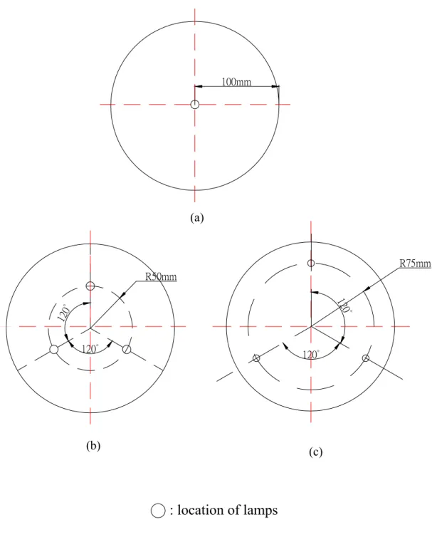
(30) 100mm. (a). R75mm R50mm. °. 120. °. 120. 120°. 120°. (b). (c). : location of lamps. Fig. 2.2. Schematic of the heating lamp arrangement : (a)one lamp, (b)three lamps-first arrangement, and (c)three lamps-second arrangement.. 12.
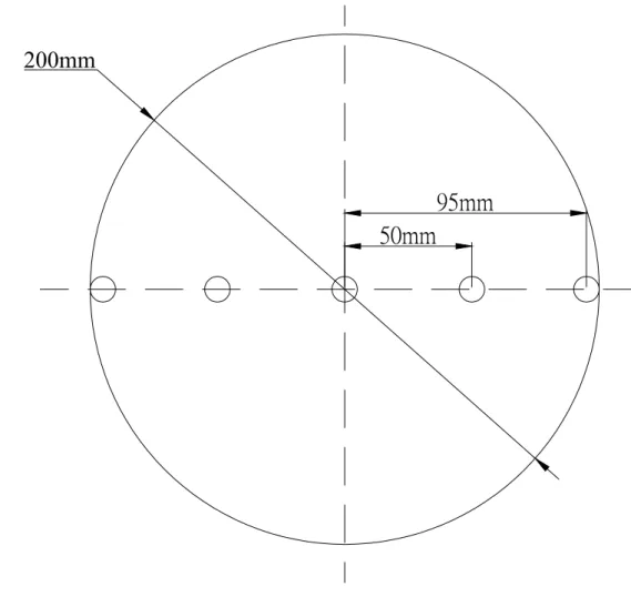
(31) 200mm. 95mm 50mm. Fig. 2.3. Schematic of the selected detection locations for the wafer temperature measurement.. 13.
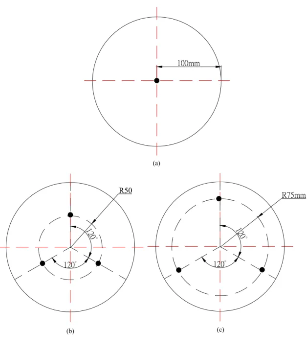
(32) 100mm. (a). R50. R75mm. 120. °. °. 120. 120°. 120°. (b). (c). = control points of feedback. Fig. 2.4. Schematic of the feedback control points on the wafer with (a)one lamp , (b)three lamps-first arrangement, and (c)three lamps-second arrangement.. 14.
(33) Lamp Stand. Shield. Lamp Wafer. H Shaft. ω Fig. 2.5. Schematic diagram of the rotation unit. 15. Susceptor.
(34) Wafer. Base. Ball Bearing. Sensor. Screw Board translation Fig. 2.6. Schematic diagram of the translation unit. 16. Translation motor.
(35) 0 R8 R10. 0. 30. 10. 19 5. 1. 5. 10. R1 2 0. wafer. pin cylinder 5. 10. 15. 5. 30 19. Unit:mm Fig. 2.7 Schematic diagram of the susceptor. 17.
(36) 18.
(37) CHAPTEER 3. UNCERTAINTY ANALYSIS. An uncertainty analysis is carried out here to estimate the uncertainty levels in the experiment. Kline and McClintock [45] proposed a formula for evaluating the uncertainty. in. the. X , X ..................... X n 1 2. result. F. as. a. function. of. independent. variables,. ,. (. F=F. X , X 2 , X 3 ,⋅ ⋅ ⋅ ⋅ ⋅ ⋅ ⋅ ⋅ X n 1. ). (3.1). The absolute uncertainty of F is expressed as 1 2. 2 2 2 2⎫ ⎧ ⎡⎛ ∂F ⎞ ⎤ ⎪ ⎪⎡⎛⎜ ∂F ⎞⎟ ⎤ ⎡⎛⎜ ∂F ⎞⎟ ⎤ ⎡⎛⎜ ∂F ⎞⎟ ⎤ ⎜ ⎟ δF = ⎨ ⎢ ⎜ ∂X ⎟δX1 ⎥ + ⎢⎜ ∂X ⎟δX 2 ⎥ + ⎢⎜ ∂X ⎟δ X3⎥ + .... + ⎢⎜ ∂X ⎟δX n ⎥ ⎬ ⎪⎣⎢⎝ 1 ⎠ ⎦⎥ ⎣⎢⎝ 2 ⎠ ⎦⎥ ⎣⎢⎝ 3 ⎠ ⎦⎥ ⎣⎢⎝ n ⎠ ⎦⎥ ⎪ ⎩ ⎭. (3.2). and the relative uncertainty of F is 1 2. δF F. If. δF F. 2 2 2⎫ ⎧ ⎡⎛ ∂ ln F ⎞⎛ δX n ⎞⎤ ⎪ ⎪⎡⎛⎜ ∂ ln F ⎞⎟⎛⎜ δX1 ⎞⎟⎤ ⎡⎛⎜ ∂ ln F ⎞⎟⎛⎜ δX 2 ⎞⎟⎤ ⎜ ⎟ ⎜ ⎟ = ⎨⎢ ⎜ ∂ ln X ⎟⎜ X ⎟⎥ + ⎢⎜ ∂ ln X ⎟⎜ X ⎟⎥ + .... + ⎢⎜ ∂ ln X ⎟⎜ X ⎟⎥ ⎬ ⎥ ⎪ ⎥ ⎥ ⎣⎢⎝ 1 ⎠⎝ 1 ⎠⎦ 2 ⎠⎝ 2 ⎠⎦ n ⎠⎝ n ⎠⎦ ⎪⎣⎢⎝ ⎣⎢⎝ ⎩ ⎭. F = X1a X b2 X 3c ........ , then the relative uncertainty is. 2 2 ⎡ δX 2 ⎤ ⎛ δX 2 ⎞ ⎛ δX3 ⎞ ⎛ 1⎞ ⎥ = ⎢⎜ a + b + c + ....... ⎟ ⎟ ⎜ ⎟ ⎜ ⎢⎝ X1 ⎠ ⎝ X 2 ⎠ ⎝ X3 ⎠ ⎥ ⎣ ⎦. Where. (. ∂F / ∂X. i. (3.3). ) and. δX i. 1 2. (3.4). are, respectively, the sensitivity coefficient and uncertainty. level associated with the variable X i . The values of the uncertainty intervals δXi are 18.
(38) obtained by a root-mean-square combination of the precision uncertainty of the instruments and the unsteadiness uncertainty, as recommended by Moffat [46]. The choice of the variable X i to be included in the calculation of the total uncertainty level of the result F depends on the purpose of the analysis. The uncertainties for the chosen parameters are calculated as follows: (1) Uncertainty of the measured temperature difference, ∆ T = T w − Ta. δ(Tw − Ta ) = [(δTw ) 2 + (δTa ) 2 ]. 1. (3.5). 2. (2) The dependence of the air properties k, µ, and ν on the temperature ( T in K ) is [47] k = 1.195 × 10 −6 T1.6 /(T + 118) µ = 1.448 × 10 −6 T 1.5 /(T + 118). (3.6). ν = µ/ρ. The uncertainties of the properties are. δk T ∂k δT = k k ∂T T δρ T ∂ρ δT = ρ ρ ∂T T δµ T ∂µ δT = µ µ ∂T T. (3.7). (3) Uncertainty of Rayleigh number, Ra, gβ(Tw − T a ) H 3 gβ∆T H 3 Ra = = αν αν. (3.8). δRa ⎡⎛ δgβ ⎞ ⎛ δH ⎞ ⎛ δ∆T ⎞ ⎛ δα ⎞ ⎛ δν ⎞ ⎟ + ⎜3 = ⎜ ⎟ +⎜ ⎟ +⎜ ⎟ ⎟ +⎜ Ra ⎢⎜⎝ gβ ⎟⎠ ⎝ H ⎠ ⎝ ∆T ⎠ ⎝ α ⎠ ⎝ ν ⎠ ⎣ 2. 2. 2. 2. 2. ⎤ ⎥⎦. The results from this uncertainty analysis are summarized in Table .3.1.. 19. 1/ 2. (3.9).
(39) Table 3.1 Summary of uncertainty analysis.. Parameters. Uncertainty. H. ±0.001 m. D. ±0.01 m. ω. ±5 rpm. Dw (m). ±0.00005 m. Tw , ΔTmax (℃). ±0.3℃. ΔT(%). 0.1%. 20.
(40) CHAPTER 4. RESULTS AND DISCUSSION. Selected data obtained in the present study are presented in the following to show how the wafer rotation, wafer translation and lamp-to-wafer separation distance level affect the silicon wafer temperature uniformity during the ramp-up period for the different power levels. In the experiment the rotation speed of wafer ω is varied from 0 to 200 rpm (revolutions per minute), and the lamp-to-wafer separation distance H is fixed at 30 mm, 60 mm or 90 mm with the translating speed of the wafer Vd varied from 0 to 15 mm/s. The wafer is heated by one or three lamps. To signify the improvement in the wafer temperature uniformity by the wafer rotation and translation, we introduce a wafer temperature nonuniformity function Φ based on the reduction in the maximum detected temperature difference on the wafer. The function is defined as. ⎛ ∆Tmax ⎞⎟ Φ = ⎜⎜1 − ⎟ ∗ 100% T ∆ max,o ⎠ ⎝. (4.1). where ΔTmax is the detected maximum temperature difference over the wafer during the ramp-up period for a given case and the subscript “o” denotes the condition of ω = 0 rpm and Vd = 0 mm/s. Specifically, the maximum temperature difference ΔTmax is chosen as the difference between the measured maximum wafer temperature and the average measured wafer temperature at all detection points on the wafer. Note that the instant of time when the lamps are turned on is designated as time t = 0. The wafer is heated until it reaches a preset average temperature. To simplify the test procedures, we choose to employ the average measured wafer temperature as the target 21.
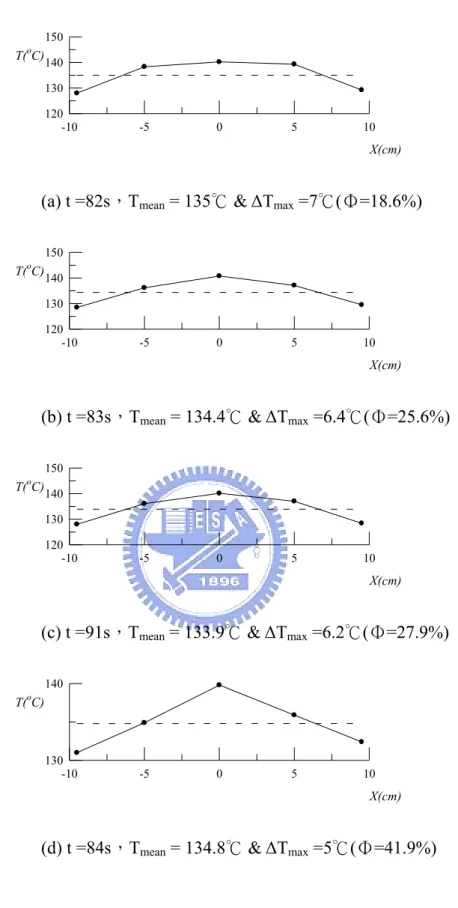
(41) temperature level for the lamp heating period. For the wafer heated by one lamp the target is 140 ℃.While for the wafer heated by three lamps the target temperature is raised to 200 ℃. Typical measured time variations of the temperature at the geometric center of the wafer are shown in Fig. 4.1 and Fig. 4.2, respectively, for the wafer heated by one lamp and three lamps. The ramp-up period ranges from 100 to 500, seconds depending on the input power and H.. 4.1 Effects of Lamp Power Level on Wafer Temperature Nonuniformity As already mentioned above, the number of lamps used in this experiment reflects the level of the power input to the wafer. The power level is expected to be an important factor for the wafer temperature uniformity. Thus before examining the effects of the wafer rotation and translation, the influences of the power level on the wafer temperature uniformity are discussed. At first, selected data from the wafer temperature measurements for the case with a single heating lamp and no wafer rotation and translation (ω=0, Vd=0) are shown in Fig. 4.3. The results indicate that in the initial stage of the ramp-up period the maximum temperature difference among the temperature detection locations is low. For example, at t =20 sec the maximum temperature difference ΔTmax is 3.6 ℃ (Fig. 4.3(a)) and at this instant of time the average wafer temperature Tmean is also low at 55.6 ℃, indicating that we have relatively small temperature nonuniformity at this early stage of wafer heating. But slightly later at t = 40 sec the maximum temperature difference increases substantially to 7.1 ℃ with Tmean = 85.1 ℃ (Fig. 4.3(b)). A further increase in ΔTmax is noted for the continuing heating up of the wafer with time. At t = 81 sec we have a relatively large temperature nonuniformity with ΔTmax = 8.6 ℃ (Fig. 4.3(d)). We also note that the temperature is higher in the region near the geometric center of the wafer and 22.
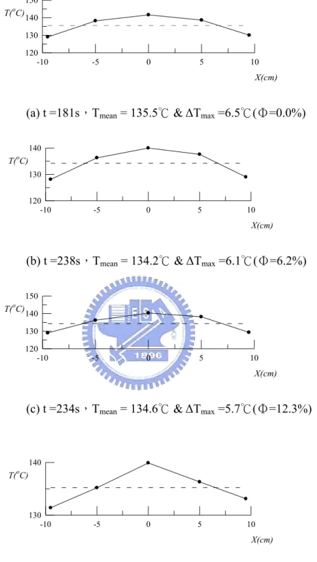
(42) lower in the region near the wafer edge, implying the larger heat loss from the wafer edge. Besides, near the geometric center the wafer receives more thermal radiation from the lamp. Similar trend is noted for other cases shown in Fig. 4.4 for the wafer heated by three lamps at the same H, ω and Vd. Moreover, the wafer temperature nonuniformity is also highest in the final stage of the wafer ramp-up process. This obviously results from the fact that the wafer temperature near the geometric center rises at a faster rate than the wafer edge. For the wafer heated by three lamps arranged as Fig. 2.2(b) (Fig. 4.4), the maximum temperature difference across the wafer is significantly higher, reflecting the higher power input to the wafer. However, at this higher power input the wafer is ramped up quicker.. 4.2 Effects of Wafer Rotation Speed on Wafer Temperature Uniformity The temperature uniformity of the wafer affected by the rotation rate of the wafer is shown in Fig. 4.5 by presenting the measured wafer temperature at selected locations when the target temperature of the wafer heated by one lamp reaches 140 ℃ for various ω for H=30 mm and Vd=0 mm/s. At ω= 0 rpm, the measured maximum temperature difference across the wafer is 8.6 ℃ and Φ defined in Eq.(4.1) is equal to 0﹪(Fig. 4.5(a)) and at this instant of time the mean wafer temperature Tmean = 133.3℃. For the rotational speed raised slightly to 50 rpm the maximum temperature difference across the wafer reduces to 7.7 ℃. and hence the temperature. nonuniformity is reduced by 10.5﹪ when compared with that for ω= 0 rpm (Fig.4.5 (b)). A further reduction in ΔTmax is noted for a continuing increase in the rotational speed of the wafer. At ω = 150 rpm we have a still smaller temperature nonuniformity with ΔTmax = 6.5 ℃ and the wafer temperature nonuniformity is reduced by 24.4﹪(Fig. 4.5(d)). For a further increase of the rotational speed of the 23.
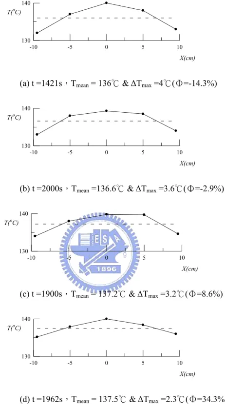
(43) wafer to 200 rpm (ω=200 rpm), we have ∆Tmax = 7.7 ℃ and the wafer temperature uniformity becomes worse with Φ = 10.5% (Fig. 4.5(e)). In other words the wafer temperature nonuniformity increases as ω is raised from 150 to 200 rpm. From the results in Fig. 4.5 the temperature uniformity of the wafer improves with increasing rotation speed of the susceptor before ω reaches 150 rpm. Moreover, the results also manifest that the symmetry of the wafer temperature distribution can be somewhat improved by increasing the rotational speed of the wafer. The measured data for other H and Vd shown in Figs. 4.6 - 4.12 also exhibit a similar trend for the variation of the wafer temperature uniformity with the wafer rotation rate. Note that for case with H = 60.0 mm, ω = 150 rpm and Vd = 15 mm/s the wafer temperature uniformity can be improved up to 66.2﹪, as evident from the results in Fig. 4.12(d). When the wafer is heated by three lamps arranged as Fig. 2.2 (b), the data given in Fig. 4.13 – 4.20 also indicate that improvement in the wafer temperature uniformity can be obtained by increasing the wafer rotation rate for ω up to 150 rpm. For ω> 150 rpm an opposite effect is noted.. 4.3 Effects of Wafer Translation on Wafer Temperature Uniformity Selected data are presented in Figs. 4.21 – 4.29 to illustrate the wafer temperature uniformity affected by the translation of the wafer heated by a single lamp. Figure 4.21 shows that at ω = 0 rpm and H = 60 mm a better wafer temperature uniformity is obtained at a higher wafer translation speed. Specifically, at Vd = 15 mm/s the wafer temperature nonuniformity can be reduced by 24.6% when compared with that at ω=0 and Vd=0. Note that the wafer translation exhibits a pronounced effect on the wafer temperature uniformity at the higher wafer rotation rate of 100 rpm (Fig. 4.22). A reduction of 58.5﹪ in the wafer temperature nonuniformity results for Vd = 15 mm/s (Fig. 4.22(d)). At an even higher ω of 200 24.
(44) rpm the wafer temperature uniformity is also better at a higher Vd. But the degree of improvement is not so high when compared with that for ω = 100 rpm. (Fig. 4.23) The results for H = 30 mm & 90 mm given in Figs. 4.24 – 4.29 also show a similar trend. When the wafer is heated by three lamps, the wafer translation can also improve the wafer temperature uniformity noticeably, as evident from the data given in Figs. 4.30 – 4.38. But the degree of the wafer temperature uniformity is slightly less when compared with the cases of a single lamp heating. This obviously results from the higher power level for the wafer heated by three lamps.. 4.4 Effects of Lamp-to-Wafer Separation Distance on Wafer Temperature Uniformity The results presented in the previous sections clearly indicate that the lamp-to-wafer separation distance is an important factor in influencing the wafer temperature uniformity and hence needs to be examined. This is illustrated in Figs. 4.39 – 4.62 by presenting the data for various H at fixed ω and Vd for the wafer heated by a single lamp and by three lamps. The results distinctly show that increasing lamp-to-wafer separation distance can improve the wafer temperature uniformity to a significant degree. For instance, at ω = 0 rpm and Vd = 0 mm/s the wafer temperature nonuniformity is reduced by 59.3﹪ when H is increased from 30 to 90 mm for the wafer subjected to one lamp heating (Fig. 4.39). At a high ω of 100 rpm Fig. 4.40 shows that the reduction in the wafer temperature nonuniformity is raised to 73.3﹪. Note that at ω = 100 rpm and Vd = 15 mm/s the improvement in the wafer temperature uniformity can be up to 87.2﹪ (Fig. 4.49). Now the data give in Figs. 4.51 – 4.62 for the wafer heated by three lamps also manifest that increasing the lamp-to-wafer separation distance significantly improves the wafer temperature 25.
(45) uniformity. Even at ω= 0 rpm the reduction in Φ due to H raised from 30 mm to 90 mm is relatively substantial with Φ all larger than 70﹪(Figs. 4.51, 4.54, 4.57 and 4.60). The significant reduction in the wafer temperature nonuniformity with an increase in the lamp-to-wafer separation distance can be attributed to the fact that at a higher H the thermal radiation emitted from the lamps distributes more uniformly on the wafer surface. Meanwhile the thermal radiation flux on the wafer is less at a higher H and thus the ramp-up period of the wafer is longer.. 4.5 Effects of Lamp Arrangement on Wafer Temperature Uniformity In the above discussion, we realize that the wafer temperature uniformity for the wafer heated by a single lamp is somewhat better than that by three lamps. It is legitimate to suspect that this is caused by the relatively nonuniform thermal radiation emitted from the three lamps arranged as that schematically shown in Fig. 2.2(b). Therefore tests are conducted for the wafer heated by a different arrangement of the three lamps as that schematically shown in Fig. 2.2(c), with the lamps located at a longer distance away from the axis of the processor. The data for the measured wafer temperature during the ramp-up period for these two lamp arrangements for ω=0 rpm and Vd= 0 mm/s are given in Figs. 4.63 and 4.64. The results indicate that when the lamps are slightly more separated from each other the wafer temperature is more uniform. This is considered to result from the fact that for the lamp arrangement shown in Fig. 2.2(c) the thermal radiation incident on the wafer is less nonuniform as compared with that for Fig. 2.2 (b). We further illustrate the effects of the lamp arrangement on the wafer temperature uniformity for the wafer rotated at different rates by comparing the data in Figs. 4.14 and 4.65 for Vd = 0 mm/s. The results also indicate that separating the lamps slightly away from each other can improve the wafer temperature uniformity even when the wafer is under rotation. Similar 26.
(46) conclusion is noted when the wafer is under rotation and translation, as evident from the results in Figs. 4.20 and 4.66.. 4.6 Optimal Condition for Wafer Temperature Uniformity The results presented above distinctly suggest that the wafer temperature uniformity can be improved by increasing the lamp-to-wafer separation distance and wafer translating speed for the wafer rotated at certain rate. Besides, the wafer heated by a single lamp is at a more uniform temperature. An attempt is made here to search for the optimal condition for the wafer temperature uniformity subjected to the constraints of the present experimental system. In this seach ω is tested at an interval of 10 rpm and Vd at an interval of 1 mm/s. The results indicate that at ω= 170 rpm and Vd = 17 mm/s for H= 90.0 mm the wafer temperature uniformity can be reduced by 85.7 % for the wafer heated by a single lamp. The data are shown in Fig. 4.67. Note that at this optimal condition △Tmax is as low as 0.5℃.. 27.
(47) o. T( C) 160.00 140.00. 120.00. 100.00. 80.00. 60.00. 40.00. 20.00. 0.00 0.00. 100.00. 200.00. 300.00. 400.00. 500.00. t (s). Fig. 4.1 Time variation of the wafer temperature measured at the geometric center of the wafer during the ramp-up period for the wafer heated by a single lamp for H= 90 mm, ω= 150 rpm, and Vd = 15 mm/s.. 28.
(48) o. T( C). 250.00. 200.00. 150.00. 100.00. 50.00. 0.00 0.00. 20.00. 40.00. 60.00. 80.00. 100.00. t (s). Fig. 4.2 Time variation of the wafer temperature measured at the geometric center of the wafer during the ramp-up period for the wafer heated by three lamps arranged as Fig. 2.2(b) for H= 60 mm, ω= 150 rpm, and Vd = 15 mm/s.. 29.
(49) 60. T(oC). 50 -10. -5. 0. 5. 10. X(cm). (a) t =20s,Tmean =55.6℃ & ∆Tmax =3.6℃ 100. T(oC). 90 80 70 -10. -5. 0. 5. 10. X(cm). (b) t =40s,Tmean = 85.1℃ & ∆Tmax =7.1℃ 120. T(oC) 110 100 -10. -5. 0. 5. 10. X(cm). (c) t = 60s,Tmean =122.2℃ & ∆Tmax =7.2℃ 150. T(oC). 140 130 120 -10. -5. 0. 5. 10. X(cm). (d) t =81s,Tmean = 133.3℃ & ∆Tmax =8.6℃. Fig. 4.3 The measured wafer temperature at selected locations for H=30 mm,Vd= 0 mm/s and ω=0 rpm for the wafer heated by one lamp during the ramp-up period. 30.
(50) 60 o. T( C) 50 40 -10. -5. 0. 5. 10. X(cm). (a) t = 10s,Tmean = 48.1℃ & ∆Tmax =6.6℃ 110 o. T( C) 100 90 80 70 -10. -5. 0. 5. 10. X(cm). (b) t = 20s,Tmean = 91.4℃ & ∆Tmax =15.1℃ 160 150 T( C) 140 130 120 110 -10 o. -5. 0. 5. 10. X(cm). (c) t = 30s,Tmean =134.9℃ & ∆Tmax =21.3℃ 210 T( C) 200 190 180 170 160 150 -10 o. -5. 0. 5. 10. X(cm). (d) t = 40s,Tmean = 174.4℃ & ∆Tmax =26℃. Fig. 4.4 The measured wafer temperature at selected locations for H=30 mm,Vd= 0 mm/s and ω=0 rpm for the wafer heated by three lamps during the ramp-up period.. 31.
(51) 150 o. T( C). 140 130 120 -10. -5. 0. 5. 10. X(cm). (a)ω= 0rpm, t =81s,Tmean = 133.3℃ & ΔTmax =8.6℃(Φ=0%) 150 o. T( C). 140 130 120 -10. -5. 0. 5. 10. X(cm). (b)ω= 50rpm, t =82s,Tmean = 134.7℃ & ΔTmax =7.7℃(Φ=10.5%) 150 o. T( C). 140 130 120 -10. -5. 0. 5. 10. X(cm). (c)ω= 100rpm, t =82s,Tmean = 135℃ & ΔTmax =7℃(Φ=18.6%) 140. T(oC) 130 120 -10. -5. 0. 5. 10. X(cm). (d)ω= 150rpm, t =90s,Tmean = 134.7℃ & ΔTmax =6.5℃(Φ=24.4%) 140. T(oC) 130 120 -10. -5. 0. 5. 10. X(cm). (e)ω=200rpm, t =94s,Tmean = 132.2℃ & ΔTmax =7.7℃(Φ=10.5%). Fig. 4.5. The measured wafer temperature at selected locations for (a) ω= 0 rpm, (b) ω= 50 rpm, (c) ω= 100 rpm, (d) ω= 150 rpm and (e)ω= 200 rpm at H= 30 mm and Vd=0 mm/s for the wafer heated by one lamp.. 32.
(52) 140. T(oC) 130 120 -10. -5. 0. 5. 10. X(cm). (a)ω= 0rpm, t =126s,Tmean = 135.5℃ & ∆Tmax =6.5℃(Φ=0.0%) 140. T(oC) 130 120 -10. -5. 0. 5. 10. X(cm). (b)ω= 50rpm, t =134s,Tmean = 135.4℃ & ∆Tmax =6.4℃(Φ=1.5%) 150. T(oC) 140 130 -10. -5. 0. 5. 10. X(cm). (c)ω= 100rpm, t =154s,Tmean = 136.4℃ & ∆Tmax =5.4℃(Φ=16.9%) 140. T(oC). 130 -10. -5. 0. 5. 10. X(cm). (d)ω= 150rpm, t =152s,Tmean = 136.7℃ & ∆Tmax =4.7℃(Φ=27.7%) 150. T(oC). 140 130 120 -10. -5. 0. 5. 10. X(cm). (e)ω= 200rpm, t =181s,Tmean = 135.5℃ & ∆Tmax =6.5℃(Φ=0%). Fig. 4.6. The measured wafer temperature at selected locations for (a) ω= 0 rpm, (b) ω= 50 rpm, (c) ω= 100 rpm, (d) ω= 150 rpm and (e)ω= 200 rpm at H= 60 mm and Vd=0 mm/s for the wafer heated by one lamp.. 33.
(53) 150. T(oC). 140 130 120 -10. -5. 0. 5. 10. X(cm). (a)ω= 0rpm, t =81s,Tmean = 132.5℃ & ∆Tmax =7.8℃(Φ=9.3%) 150. T(oC). 140 130 120 -10. -5. 0. 5. 10. X(cm). (b)ω= 50rpm, t =82s,Tmean = 132.9℃ & ∆Tmax =7.3℃(Φ=15.1%) 150. T(oC). 140 130 120 -10. -5. 0. 5. 10. X(cm). (c)ω=100rpm, t =83s,Tmean = 134.4℃ & ∆Tmax =6.4℃(Φ=25.6%) 140. T(oC) 130 120 -10. -5. 0. 5. 10. X(cm). (d)ω= 150rpm, t =86s,Tmean = 135.1℃ & ∆Tmax =5.6℃(Φ=34.9%) 140. T(oC) 130 120 -10. -5. 0. 5. 10. X(cm). (e)ω=200rpm, t =99s,Tmean = 131.6℃ & ∆Tmax =8.3℃(Φ=3.5%). Fig. 4.7 The measured wafer temperature at selected locations for (a) ω= 0 rpm, (b) ω= 50 rpm, (c) ω= 100 rpm, (d) ω= 150 rpm and (e)ω= 200 rpm at H= 30 mm and Vd=5 mm/s for the wafer heated by one lamp.. 34.
(54) 140. T(oC) 130 120 -10. -5. 0. 5. 10. X(cm). (a)ω= 0rpm, t =163s,Tmean = 134.1℃ & ∆Tmax =5.8℃(Φ=10.8%) 150. T(oC) 140 130 -10. -5. 0. 5. 10. X(cm). (b)ω= 50rpm, t =154s,Tmean = 135.6℃ & ∆Tmax =4.7℃(Φ=27.7%) 140. T(oC). 130 -10. -5. 0. 5. 10. X(cm). (c)ω=100rpm, t =184s,Tmean =136.2℃ & ∆Tmax =4.1℃(Φ=36.9%) 140. T(oC). 130 -10. -5. 0. 5. 10. X(cm). (d)ω= 150rpm, t =198s,Tmean = 136.8℃ & ∆Tmax =3.5℃(Φ=46.2%) 140. T(oC) 130 120 -10. -5. 0. 5. 10. X(cm). (e)ω= 200rpm, t =238s,Tmean = 134.2℃ & ∆Tmax =6.1℃(Φ=6.2%). Fig. 4.8 The measured wafer temperature at selected locations for (a) ω= 0 rpm, (b) ω= 50 rpm, (c) ω= 100 rpm, (d) ω= 150 rpm and (e)ω= 200 rpm at H= 60 mm and Vd=5 mm/s for the wafer heated by one lamp.. 35.
(55) 150. T(oC). 140 130 120 -10. -5. 0. 5. 10. X(cm) ( (a)ω= 0rpm, t =91s,Tmean = 133.2℃ & ΔTmax =7.4℃(Φ=14.0%). 150. T(oC). 140 130 120 -10. -5. 0. 5. 10. X(cm). (b)ω= 50rpm, t =88s,Tmean = 133.7℃ & ΔTmax =6.9℃(Φ=19.8%) 150. T(oC). 140 130 120 -10. -5. 0. 5. 10. X(cm). (c)ω= 100rpm, t =91s,Tmean = 133.9℃ & ΔTmax =6.2℃(Φ=27.9%) 150. T(oC) 140 130 -10. -5. 0. 5. 10. X(cm). (d)ω= 150rpm, t =92s,Tmean = 135.1℃ & ΔTmax =5.3℃(Φ=38.9%) 150. T(oC). 140 130 120 -10. -5. 0. 5. 10. X(cm). (e)ω= 200rpm, t =104s,Tmean = 131℃ & ΔTmax =9.4℃(Φ=-9.3%). Fig. 4.9 The measured wafer temperature at selected locations for (a) ω= 0 rpm, (b) ω= 50 rpm, (c) ω= 100 rpm, (d) ω= 150 rpm and (e)ω= 200 rpm at H= 30 mm and Vd=10 mm/s for the wafer heated by one lamp. 36.
(56) 140 o. T( C) 130 120 -10. -5. 0. 5. 10. X(cm). (a)ω= 0rpm, t =157s,Tmean = 134.5℃ & ∆Tmax =5.6℃(Φ=17.8%) 140. T(oC). 130 -10. -5. 0. 5. 10. X(cm). (b)ω= 50rpm, t =174s,Tmean = 136℃ & ∆Tmax =4.2℃(Φ=35.4%) 150 o. T( C) 140 130 -10. -5. 0. 5. 10. X(cm). (c)ω= 100rpm, t =184s,Tmean = 138.1℃ & ∆Tmax =3.2℃(Φ=50.8%) 140 o. T( C). 130 -10. -5. 0. 5. 10. X(cm). (d)ω= 150rpm, t =237s,Tmean = 137.2℃ & ∆Tmax =2.7℃(Φ=58.5%) 150 o. T( C). 140 130 120 -10. -5. 0. 5. 10. X(cm). (e)ω= 200rpm, t =234s,Tmean = 134.6℃ & ∆Tmax =5.7℃(Φ=12.3%). Fig. 4.10 The measured wafer temperature at selected locations for (a) ω= 0 rpm, (b) ω= 50 rpm, (c) ω= 100 rpm, (d) ω= 150 rpm and (e)ω= 200 rpm at H= 60 mm and Vd=10 mm/s for the wafer heated by one lamp. 37.
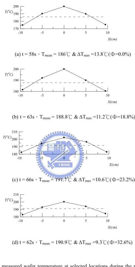
(57) 150 o. T( C). 140 130 120 -10. -5. 0. 5. 10. X(cm). (a)ω= 0rpm, t =84s,Tmean = 133.5℃ & ∆Tmax =6.9℃(Φ=19.8%) 140 o. T( C). 130 -10. -5. 0. 5. 10. X(cm). (b)ω= 50rpm, t =82s,Tmean = 134.2℃ & ∆Tmax =5.6℃(Φ=34.8%) 140. T(oC). 130 -10. -5. 0. 5. 10. X(cm). (c)ω= 100rpm, t =84s,Tmean = 134.8℃ & ∆Tmax =5℃(Φ=41.9%) 150. T(oC) 140 130 -10. -5. 0. 5. 10. X(cm). (d)ω= 150rpm, t =87s,Tmean = 136℃ & ∆Tmax =4.3℃(Φ=50.0%) 140. T(oC) 130 120 -10. -5. 0. 5. 10. X(cm). (e)ω= 200rpm, t =91s,Tmean = 132.4℃ & ∆Tmax =7.4℃(Φ=14.0%). Fig. 4.11 The measured wafer temperature at selected locations for (a) ω= 0 rpm, (b) ω= 50 rpm, (c) ω= 100 rpm, (d) ω= 150 rpm and (e)ω= 200 rpm at H= 30 mm and Vd=15 mm/s for the wafer heated by one lamp. 38.
(58) 150 o. T( C) 140 130 -10. -5. 0. 5. 10. X(cm). (a)ω= 0rpm, t =161s,Tmean = 135.4℃ & ∆Tmax =4.9℃(Φ=24.6%) 150 o. T( C) 140 130 -10. -5. 0. 5. 10. X(cm). (b)ω= 50rpm, t =176s,Tmean = 136.6℃ & ∆Tmax =3.5℃(Φ=46.2%) 140 o. T( C). 130 -10. -5. 0. 5. 10. X(cm). (c)ω= 100rpm, t =172s,Tmean = 137.3℃ & ∆Tmax =2.7℃(Φ=58.5%) 140 o. T( C). 130 -10. -5. 0. 5. 10. X(cm). (d)ω= 150rpm, t =204s,Tmean = 137.8℃ & ∆Tmax =2.2℃(Φ=66.2%) 140. T(oC). 130 -10. -5. 0. 5. 10. X(cm). (e)ω= 200rpm, t =328s,Tmean = 135.2℃ & ∆Tmax =4.8℃(Φ=26.2%). Fig. 4.12 The measured wafer temperature at selected locations for (a) ω= 0 rpm, (b) ω= 50 rpm, (c) ω= 100 rpm, (d) ω= 150 rpm and (e)ω= 200 rpm at H= 60 mm and Vd=15 mm/s for the wafer heated by one lamp. 39.
(59) 210 T( C) 200 190 180 170 160 150 -10 o. -5. 0. 5. 10. X(cm). (a)ω= 0rpm, t = 40s,Tmean = 174.4℃ & ∆Tmax =26℃(Φ=0%) 200 o. T( C) 190 180 170 160 -10. -5. 0. 5. 10. X(cm). (b)ω= 50rpm, t = 40s,Tmean = 177.2℃ & ∆Tmax =22.2℃(Φ=14.6%) 210 200 T( C) 190 180 170 160 -10 o. -5. 0. 5. 10. X(cm). (c)ω=100rpm, t = 40s,Tmean = 180.4℃ & ∆Tmax =19.7℃(Φ=24.2%) 210 200 T( C) 190 180 170 160 -10 o. -5. 0. 5. 10. X(cm). (d)ω=150rpm, t = 38s,Tmean = 181.5℃ & ∆Tmax =18.6℃(Φ=28.5%) 200 o. T( C) 190 180 170 160 -10. -5. 0. 5. 10. X(cm). (e)ω=200rpm, t = 62s,Tmean = 177.9℃ & ∆Tmax =21.9℃(Φ=15.8%). Fig. 4.13 The measured wafer temperature at selected locations for (a) ω= 0 rpm, (b) ω= 50 rpm, (c) ω= 100 rpm, (d) ω= 150 rpm and (e)ω= 200 rpm at H= 30 mm and Vd=0 mm/s for the wafer heated by three lamps. 40.
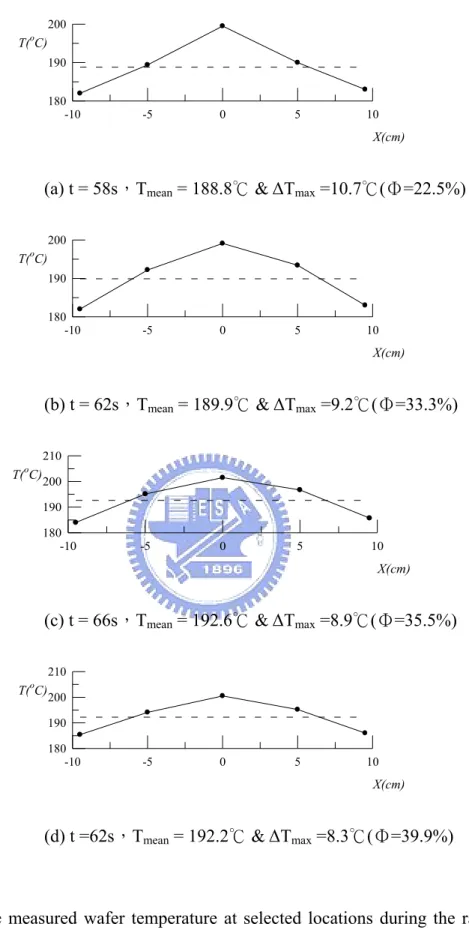
(60) 200 o. T( C). 190 180 170 -10. -5. 0. 5. 10. X(cm). (a)ω= 0rpm, t = 58s,Tmean = 186℃ & ∆Tmax =13.8℃(Φ=0%) 200 o. T( C). 190 180 170 -10. -5. 0. 5. 10. X(cm). (b)ω= 50rpm, t = 58s,Tmean = 188.2℃ & ∆Tmax =11.8℃(Φ=14.5%) 200 o. T( C) 190 180 -10. -5. 0. 5. 10. X(cm). (c)ω=100rpm, t = 58s,Tmean = 188.8℃ & ∆Tmax =10.7℃(Φ=22.5%) 200 o. T( C) 190 180 -10. -5. 0. 5. 10. X(cm). (d)ω=150rpm, t = 59s,Tmean = 189.5℃ & ∆Tmax =10.2℃(Φ=26.1%) 200 o. T( C). 190 180 170 -10. -5. 0. 5. 10. X(cm). (e)ω=200rpm, t = 60s,Tmean = 187.8℃ & ∆Tmax =11.6℃(Φ=15.9%). Fig. 4.14 The measured wafer temperature at selected locations for (a) ω= 0 rpm, (b) ω= 50 rpm, (c) ω= 100 rpm, (d) ω= 150 rpm and (e)ω= 200 rpm at H= 60 mm and Vd=0 mm/s for the wafer heated by three lamps.. 41.
(61) 200. T(oC) 190 180 170 160 -10. -5. 0. 5. 10. X(cm). (a)ω= 0rpm, t = 44s,Tmean = 176.2℃ & ∆Tmax =23.7℃(Φ=8.9%) 200. T(oC) 190 180 170 160 -10. -5. 0. 5. 10. X(cm). (b)ω= 50rpm, t = 43s,Tmean = 179.3℃ & ∆Tmax =20.7℃(Φ=20.4%) 210. T(oC) 200. 190 180 170 160 -10. -5. 0. 5. 10. X(cm). (c)ω=100rpm, t = 42s,Tmean = 181.9℃ & ∆Tmax =18.7℃(Φ=28.1%) 200. T(oC) 190 180 170 160 -10. -5. 0. 5. 10. X(cm). (d)ω=150rpm, t = 41s,Tmean =180.3℃ & ∆Tmax =17.9℃(Φ=31.1%) 200 o. T( C) 190 180 170 160 -10. -5. 0. 5. 10. X(cm). (e)ω=200rpm, t = 41s,Tmean = 177.8℃ & ∆Tmax =21.1℃(Φ=22.8%). Fig. 4.15 The measured wafer temperature at selected locations for (a) ω= 0 rpm, (b) ω= 50 rpm, (c) ω= 100 rpm, (d) ω= 150 rpm and (e)ω= 200 rpm at H= 30 mm and Vd=5 mm/s for the wafer heated by three lamps.. 42.
(62) 200. T(oC) 190 180 -10. -5. 0. 5. 10. X(cm). (a)ω= 0rpm, t = 63s,Tmean = 188.8℃ & ∆Tmax =11.2℃(Φ=18.8%) 210. T(oC). 200 190 180 -10. -5. 0. 5. 10. X(cm). (b)ω= 50rpm, t = 64s,Tmean = 190.6℃ & ∆Tmax =10.8℃(Φ=21.7%) 200. T(oC) 190 180 -10. -5. 0. 5. 10. X(cm). (c)ω= 100rpm, t = 62s,Tmean = 189.9℃ & ∆Tmax =9.2℃(Φ=37.3%) 200. T(oC) 190 180 -10. -5. 0. 5. 10. X(cm). (d)ω= 150rpm, t = 66s,Tmean = 190.7℃ & ∆Tmax =8.5(Φ=38.4%) 200 o. T( C) 190 180 -10. -5. 0. 5. 10. X(cm). (e)ω= 200rpm, t =67s,Tmean = 188.3℃ & ∆Tmax =11.1℃(Φ=19.6%). Fig. 4.16 The measured wafer temperature at selected locations for (a) ω= 0 rpm, (b) ω= 50 rpm, (c) ω= 100 rpm, (d) ω= 150 rpm and (e) ω= 200 rpm at H= 60 mm and Vd=5 mm/s for the wafer heated by three lamps. 43.
(63) 210. T(oC) 200. 190 180 170 160 -10. -5. 0. 5. 10. X(cm). (a) ω= 0rpm, t = 44s,Tmean = 181.1℃ & ∆Tmax =20℃(Φ=23.1%) 210. T(oC) 200. 190 180 170 160 -10. -5. 0. 5. 10. X(cm). (b)ω= 50rpm, t = 48s,Tmean = 181.6℃ & ∆Tmax =19.3℃(Φ=25.8%) 200. T(oC) 190 180 170 160 -10. -5. 0. 5. 10. X(cm). (c)ω=100rpm, t = 45s,Tmean = 182.2℃ & ∆Tmax =17.8℃(Φ=31.5%) 210. T(oC) 200 190 180 170 -10. -5. 0. 5. 10. X(cm). (d)ω=150rpm, t = 45s,Tmean = 184.4℃ & ∆Tmax =16.2℃(Φ=37.7%) 210. T(oC) 200. 190 180 170 160 -10. -5. 0. 5. 10. X(cm). (e)ω=200rpm, t = 44s,Tmean = 180.1℃ & ∆Tmax =20.1℃(Φ=22.7%). Fig. 4.17 The measured wafer temperature at selected locations for (a) ω= 0 rpm, (b) ω= 50 rpm, (c) ω= 100 rpm, (d) ω= 150 rpm and (e) ω= 200 rpm at H= 30 mm and Vd=10 mm/s for the wafer heated by three lamps. 44.
(64) 210. T(oC). 200 190 180 -10. -5. 0. 5. 10. X(cm). (a)ω= 0rpm, t = 66s,Tmean = 191.7℃ & ∆Tmax =10.6℃(Φ=23.2%) 210. T(oC). 200 190 180 -10. -5. 0. 5. 10. X(cm). (b)ω= 50rpm, t = 58s,Tmean =190.3℃ & ∆Tmax =10.2℃(Φ=26.1%) 210. T(oC). 200 190 180 -10. -5. 0. 5. 10. X(cm). (c)ω=100rpm, t = 66s,Tmean = 192.6℃ & ∆Tmax =8.9℃(Φ=35.5%) 200. T(oC) 190 180 -10. -5. 0. 5. 10. X(cm). (d)ω= 150rpm, t = 66s,Tmean = 191.5℃ & ∆Tmax =8.1℃(Φ=41.3%) 200. T(oC). 190 180 170 -10. -5. 0. 5. 10. X(cm). (e)ω= 200rpm, t = 68s,Tmean = 187.3℃ & ∆Tmax =10.9℃(Φ=21%). Fig. 4.18 The measured wafer temperature at selected locations for (a) ω= 0 rpm, (b) ω= 50 rpm, (c) ω= 100 rpm, (d) ω= 150 rpm and (e) ω= 200 rpm at H= 60 mm and Vd=10 mm/s for the wafer heated by three lamps. 45.
(65) 210 200 T( C) 190 180 170 160 -10 o. -5. 0. 5. 10. X(cm). (a)ω= 0rpm, t = 41s,Tmean = 181.6℃ & ∆Tmax =17.9℃(Φ=31.2%) 200 o. T( C) 190 180 170 160 -10. -5. 0. 5. 10. X(cm). (b)ω= 50rpm, t = 43s,Tmean = 179.9℃ & ∆Tmax =18.2℃(Φ=30.0%) 200. T(oC). 190 180 170 -10. -5. 0. 5. 10. X(cm). (c)ω=100rpm, t = 43s,Tmean = 182.2℃ & ∆Tmax =15.9℃(Φ=38.8%) 210. T(oC) 200 190 180 170 -10. -5. 0. 5. 10. X(cm). (d)ω=150rpm, t = 42s,Tmean = 185.9℃ & ∆Tmax =14.8℃(Φ=43.1%) 210. T(oC) 200 190 180 170 -10. -5. 0. 5. 10. X(cm). (e)ω= 200rpm, t = 44s,Tmean = 182.1℃ & ∆Tmax =19℃(Φ=26.9%) Fig. 4.19 The measured wafer temperature at selected locations for (a) ω= 0 rpm, (b) ω= 50 rpm, (c) ω= 100 rpm, (d) ω= 150 rpm and (e) ω= 200 rpm at H= 30 mm and Vd=15 mm/s for the wafer heated by three lamps. 46.
(66) 210. T(oC). 200 190 180 -10. -5. 0. 5. 10. X(cm). (a)ω= 0rpm, t = 62s,Tmean = 190.9℃ & ∆Tmax =9.3℃(Φ=32.6%) 200. T(oC) 190 180 -10. -5. 0. 5. 10. X(cm). (b)ω= 50rpm, t = 64s,Tmean = 190.7℃ & ∆Tmax =8.9℃(Φ=35.5%) 210. T(oC). 200 190 180 -10. -5. 0. 5. 10. X(cm). (c)ω= 100rpm, t =62s,Tmean = 192.2℃ & ∆Tmax =8.3℃(Φ=39.9%) 210 o. T( C). 200 190 180 -10. -5. 0. 5. 10. X(cm). (d)ω= 150rpm, t =64s,Tmean = 193.3℃ & ∆Tmax =6.8℃(Φ=50.7%) 200. T(oC) 190 180 -10. -5. 0. 5. 10. X(cm). (e)ω=200rpm, t = 65s,Tmean = 189.2℃ & ∆Tmax =10.3℃(Φ=25.4%) Fig. 4.20 The measured wafer temperature at selected locations for (a) ω= 0 rpm, (b) ω= 50 rpm, (c) ω= 100 rpm, (d) ω= 150 rpm and (e) ω= 200 rpm at H= 60 mm and Vd=15 mm/s for the wafer heated by three lamps. 47.
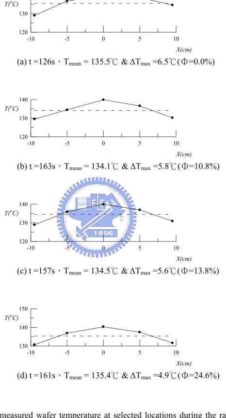
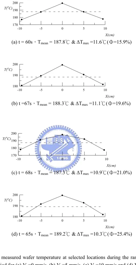
(67) 140. T(oC) 130 120 -10. -5. 0. 5. 10. X(cm). (a) t =126s,Tmean = 135.5℃ & ∆Tmax =6.5℃(Φ=0.0%). 140. T(oC) 130 120 -10. -5. 0. 5. 10. X(cm). (b) t =163s,Tmean = 134.1℃ & ∆Tmax =5.8℃(Φ=10.8%). 140. T(oC) 130 120 -10. -5. 0. 5. 10. X(cm). (c) t =157s,Tmean = 134.5℃ & ∆Tmax =5.6℃(Φ=13.8%). 150. T(oC) 140 130 -10. -5. 0. 5. 10. X(cm). (d) t =161s,Tmean = 135.4℃ & ∆Tmax =4.9℃(Φ=24.6%). Fig. 4.21 The measured wafer temperature at selected locations during the ramp-up period for (a) Vd=0 mm/s, (b) Vd=5 mm/s, (c) Vd=10 mm/s and (d) Vd=15 mm/s with the wafer heated by a single lamp at ω=0 rpm and H= 60 mm for the final wafer temperature set at 140℃. 48.
數據
+7
相關文件
• The ArrayList class is an example of a collection class. • Starting with version 5.0, Java has added a new kind of for loop called a for each
4、 0.75 mm²、1.25 mm²及 2.0 mm²的 I、O、Y
With new ICE trains crossi ng Europe at speeds of up to 300 km/h, sound and vib ration levels in the trains ar e an important issue. Hilliges/Mehrmann/Mehl(2 004) first
With new ICE trains crossing Europe at speeds of up to 300 km/h, sound and vibration levels in the trains are an important issue. Hilliges/Mehrmann/Mehl(2004) first proposed
[r]
First Taiwan Geometry Symposium, NCTS South () The Isoperimetric Problem in the Heisenberg group Hn November 20, 2010 13 / 44.. The Euclidean Isoperimetric Problem... The proof
The HDG methods are obtained by discretizing characterizations of the exact solution written in terms of many local problems, one for each element of the mesh Ω h , with suitably
• Photon mapping: trace photons from the lights d t th i h t th t b and store them in a photon map, that can be used during rendering.. Direct illumination
