行政院國家科學委員會專題研究計畫 成果報告
智慧型仿生系統之晶片系統平台技術開發--子計畫一:三
維電極感測陣列之研發(3/3)
研究成果報告(完整版)
計 畫 類 別 : 整合型 計 畫 編 號 : NSC 99-2220-E-009-019- 執 行 期 間 : 99 年 08 月 01 日至 100 年 07 月 31 日 執 行 單 位 : 國立交通大學電機與控制工程學系(所) 計 畫 主 持 人 : 邱俊誠 公 開 資 訊 : 本計畫可公開查詢中 華 民 國 100 年 11 月 24 日
中 文 摘 要 : 本子計畫目的在於發展一使用微機電技術製造的多通道 (multi-channel)三維電極感測微探針陣列,上有多個感測/ 刺激用電極以及微流道設計,可用於植入式生物訊號感測、 刺激之用。一般的多通道探針陣列多為側向式(lateral)的二 維探針設計,意即僅在同一平面做不同深度的感測,缺乏三 維立體的生物神經訊號探討。而現有文獻中的三維探針陣列 所使用的組裝方式複雜,有體積過大、組裝零件多和組裝步 驟複雜所產生的製造成本問題。本計劃所提出之三維微探針 具有較簡易的組裝方式,同時具備擴充性以及與後級處理電 路整合的能力,可以更有效的控制感測電極的位置,增加訊 號分析資料,並可進一步進行電刺激研究。由本子計畫之三 維感測電極微探針的感測電極所量測到的生物訊號資料將再 傳至其他子計畫之訊號處理以及無線傳輸電路,建構出一個 無線植入式生物訊號感測分析系統晶片平台。 中文關鍵詞: 微機電技術、微組裝、電極、三維、植入式系統 英 文 摘 要 : This project reports a new stacking method for
assembling a 3-D microprobe array. To date, 3-D array structures have usually been assembled with vertical spacers, snap fasteners and a supporting platform. Such methods have achieved 3-D structures but suffer from complex assembly steps, vertical interconnection for 3-D signal transmission, low structure strength and large implantable opening. By applying the proposed stacking method, the previous techniques could be replaced by 2-D wire bonding. In this way, supporting platforms with slots and vertical spacers were no longer needed. Furthermore, ASIC chips can be substituted for the spacers in the stacked arrays to achieve system integration, design flexibility and volume usage efficiency. To avoid overflow of the adhesive fluid during assembly, an anti-overflow design which made use of capillary action force was applied in the stacking method as well. Moreover, presented stacking procedure consumes only 35 minutes in average for a 4 × 4 3-D microprobe array without requiring other specially made assembly tools. To summarize, the advantages of the proposed stacking method for 3-D array assembly include simplified assembly process, high structure strength, smaller opening area and integration ability with active
circuits. This stacking assembly technique allows an alternative method to create 3-D structures from planar components.
英文關鍵詞: microassembly; microprobe array; three dimensional probe array
國
國科
科會
會專
專題
題研
研究
究計
計畫
畫成
成果
果報
報告
告撰
撰寫
寫格
格式
式
99 年 5 月 5 日本會第 304 次學術會報修正通過 一、說明 國科會基於學術公開之立場,鼓勵一般專題研究計畫主持人發表其研究成果,但主持 人對於研究成果之內容應負完全責任。計畫內容及研究成果如涉及專利或其他智慧財產 權、違異現行醫藥衛生規範、影響公序良俗或政治社會安定等顧慮者,應事先通知國科會 不宜將所繳交之成果報告蒐錄於學門成果報告彙編或公開查詢,以免造成無謂之困擾。另 外,各學門在製作成果報告彙編時,將直接使用主持人提供的成果報告,因此主持人在繳 交報告之前,應對內容詳細校對,以確定其正確性。 本格式說明之目的為統一成果報告之格式,精簡報告內容之篇幅以 4 至 10 頁為原則, 完整報告內容之篇幅不得少於 10 頁。 成果報告繳交之期限及種類(精簡報告、完整報告、期中精簡報告、期中完整報告等), 應依本會補助專題研究計畫作業要點及專題研究計畫經費核定清單之規定辦理。 二、報告格式:依序為封面、目錄(精簡報告得省略)、中英文摘要及關鍵詞、報告內容、參 考文獻、計畫成果自評、可供推廣之研發成果資料表、附錄。 (一)報告封面:請至本會網站(http://www.nsc.gov.tw)線上製作(格式如附件一)。 (二)中、英文摘要及關鍵詞 (keywords)。 (三)報告內容:包括前言、研究目的、文獻探討、研究方法、結果與討論(含結論與建議)… 等。 (四)計畫成果自評部分:請就研究內容與原計畫相符程度、達成預期目標情況、研究成果 之學術或應用價值(簡要敘述成果所代表之意義、價值、影響或進一步發展之可能性)、 是否適合在學術期刊發表或申請專利、主要發現或其他有關價值等,作一綜合評估, 並請至本會網站線上製作。(格式如附件二) (五)頁碼編寫:請對摘要及目錄部分用羅馬字 I 、II、 III……標在每頁下方中央;報告內 容至附錄部分請以阿拉伯數字 1.2.3.……順序標在每頁下方中央。 (六)附表及附圖可列在文中或參考文獻之後,各表、圖請說明內容。 (七)可供推廣之研發成果資料表: 1.研究計畫所產生之研發成果,應至國科會科技研發成果資訊系統(STRIKE 系統, https://nscnt66.nsc.gov.tw/strike/)填列研發成果資料表(如附件三),循執行機構行政 程序,由研發成果推廣單位(如技轉中心)線上繳交送出。 2.每項研發成果填寫一份。 (八)若該計畫已有論文發表者(頇於論文致謝部分註明補助計畫編號),得作為成果報告內 容或附錄,並請註明發表刊物名稱、卷期及出版日期。若有與執行本計畫相關之著作、 專利、技術報告、或學生畢業論文等,請在參考文獻內註明之。 三、計畫中獲補助國外或大陸地區差旅費、出席國際學術會議差旅費或國際合作研究計畫差旅 費者,頇依規定分別撰寫心得報告,並至本會網站線上繳交電子檔,心得報告格式如附件 四、五、六。 四、報告編排注意事項 (一)版面設定:A4 紙,即長 29.7 公分,寬 21 公分。 (二)格式:中文打字規格為每行繕打(行間不另留間距),英文打字規格為Single Space
。 (三)字體:以中英文撰寫均可。英文使用Times New Roman Font
,中文使用標楷體,字行政院國家科學委員會補助專題研究計畫
成果報告
□期中進度報告
智慧型仿生系統之晶片系統平台技術開發
子計畫一:三維電極感測陣列之研發
The Development of Three-Dimensional Recording
Microelectrode Arrays
計畫類別:□個別型計畫 整合型計畫
計畫編號:NSC 99-2220-E-009-019
-
執行期間: 2010 年 8 月 1 日至 2011 年 7 月 31 日
執行機構及系所:國立交通大學電機與控制工程研究所
計畫主持人:邱俊誠 教授
計畫參與人員:張志瑋 博士後研究員
成果報告類型(依經費核定清單規定繳交):□精簡報告 完整報告
本計畫除繳交成果報告外,另頇繳交以下出國心得報告:
□赴國外出差或研習心得報告
□赴大陸地區出差或研習心得報告
□出席國際學術會議心得報告
□國際合作研究計畫國外研究報告
處理方式:
除列管計畫及下列情形者外,得立即公開查詢
涉及專利或其他智慧財產權,□一年
二年後可公開查詢
中 華 民 國 年 月
附件一I
Content 目錄
Content 目錄 ... I 中文摘要... II Abstract ... III Introduction ... 1Background and paper review ... 1
Motivation ... 2
Method and Design ... 4
Result and Discussion ... 6
Reference ... 12
中文摘要
本子計畫目的在於發展一使用微機電技術製造的多通道(multi-channel)三維電極感測微探針陣列,上有 多個感測/刺激用電極以及微流道設計,可用於植入式生物訊號感測、刺激之用。一般的多通道探針陣 列多為側向式(lateral)的二維探針設計,意即僅在同一平面做不同深度的感測,缺乏三維立體的生物神 經訊號探討。而現有文獻中的三維探針陣列所使用的組裝方式複雜,有體積過大、組裝零件多和組裝 步驟複雜所產生的製造成本問題。本計劃所提出之三維微探針具有較簡易的組裝方式,同時具備擴充 性以及與後級處理電路整合的能力,可以更有效的控制感測電極的位置,增加訊號分析資料,並可進 一步進行電刺激研究。由本子計畫之三維感測電極微探針的感測電極所量測到的生物訊號資料將再傳 至其他子計畫之訊號處理以及無線傳輸電路,建構出一個無線植入式生物訊號感測分析系統晶片平台。 關鍵詞: 微機電技術、微組裝、電極、三維、植入式系統III
Abstract
This project reports a new stacking method for assembling a 3-D microprobe array. To date, 3-D array structures have usually been assembled with vertical spacers, snap fasteners and a supporting platform. Such methods have achieved 3-D structures but suffer from complex assembly steps, vertical interconnection for 3-D signal transmission, low structure strength and large implantable opening. By applying the proposed stacking method, the previous techniques could be replaced by 2-D wire bonding. In this way, supporting platforms with slots and vertical spacers were no longer needed. Furthermore, ASIC chips can be substituted for the spacers in the stacked arrays to achieve system integration, design flexibility and volume usage efficiency. To avoid overflow of the adhesive fluid during assembly, an anti-overflow design which made use of capillary action force was applied in the stacking method as well. Moreover, presented stacking procedure consumes only 35 minutes in average for a 4 × 4 3-D microprobe array without requiring other specially made assembly tools. To summarize, the advantages of the proposed stacking method for 3-D array assembly include simplified assembly process, high structure strength, smaller opening area and integration ability with active circuits. This stacking assembly technique allows an alternative method to create 3-D structures from planar components.
Introduction
In recent years, advance micromachined/assembled micro probe arrays with electrical stimulation/recording ability have come to play an essential role in exploring central neural systems. Simultaneous observation of a larger number of cell activities has become the general requirement to understand the nervous system [1]. Advances in neuroscience and neuroprosthetics now require microelectrode arrays that are able to access numerous neurons simultaneously with high spatial resolution [2]. Recording of the extracellular action potentials has been accomplished by surgically implanting neural probes into the target neurons of interest, which resulted from neural activities [3]. Probes that could insert a large number of recording sites into neural tissues with minimal tissue damage are therefore needed. Also, the design of the probe arrays should be optimized for an experimental purpose that an electrode diameter of a few micrometers could support single-unit recording [4].
Background and paper review
The traditional micro probes, which are made from insulated metal wires and glass micropipettes, cannot provide simultaneously multi-channel recording. The main reason is that the traditional devices function as only a single site on a single probe shaft. Some previous studies have improved the problem by thin-film lithography-based micromachining techniques since 1960s.
High-density probe arrays yielded insights into the organization and function of the neural system [5]. Silicon [6], glass [7], polymer [8] and sapphire [9] substrates have been employed as thin-film electrode probe planks. The thin-film silicon micro probe was developed many years ago for neuroscience and neural prostheses [10]. It has also been widely characterized electrically [11] and mechanically [12] for probe scaling [13], insertion force [14], tissue strain [15] and chronic brain responses [16]. The studies mentioned above provide detailed multi-channel recordings along a single plane, but lacked of full cell activity information in 3-D space [17].
To access the full cell activity that originates in the target tissue, three dimensional microprobe arrays are strongly required with precisely controlled dimensions and front-end circuitry compatibility. In other words, to achieve detailed studies of neural networks and implementation of neural prostheses, we need to access three-dimensional volumes of tissue with three-dimensional distributed recording sites. In modern neural system researches, 3D microprobe array allows the recording and mapping of the neural signal network and interconnections among the 3D brain structure. The recording and mapping would be impossible to achieve by using 2-D planar arrays [17].
2
Currents methods of fabricating three-dimensional microprobe array structures can be summarized as follows:
(1) Silicon bulk etched microprobe array (2) polymer-constructed array
(3) Creating 3-D arrays by the assembling of 2-D parts
For the silicon bulk etched out-of-plane microprobe arrays, every probe shaft in the array only functions as a single recording site [18]. The total number of the recording sites was limited when high recording density and number are strongly required as in recent research. Moreover, when the silicon bulk etched array was integrated with active circuitries or interconnection boards [19], the minimal opening for implantation increased. Polymer-constructed arrays utilized various polymer materials to support the 3-D structure [20], but they suffered from process incompatibility with CMOS circuitry. Creating 3-D arrays by the assembly of 2-D parts is now the most popular method to construct a 3-D structure [2] [21-25]. The 2-D parts usually include 2-D arrays, vertical spacers and supporting platform. The supporting platform acts as a substrate, and the vertical spacers are erected on the supporting platform by tethers, joints and snap fasteners. The spacers fixed the 2-D arrays vertically on the supporting platform, and made the probe shafts pass through the holes of the supporting platform. The full 3-D structure is therefore like a PC motherboard. Additionally, active circuitry for signal processing can be designed and fabricated in the back-end of the 2-D arrays to achieve system integration. A unique handling method was developed in [24] for a dual-side, ultra-thin silicon substrate process to fabricate thin probe shafts without using doping etching stop technique. Moreover, stacked probes and PCBs by anisotropic conductive film create the connection for the dual-side wire routing and 3D structure. Therefore, each side of probe can be wired out separately. An alternative solution provided in [25] integrated the silicon probe with flexible ribbon cables by using thermosonic bonded gold bump. Also, a platform with bays and gold clips is designed to connect with probes, which results in an impressive 3D device. The comparison of three-dimensional microprobe arrays with some major design parameters is shown in Table 1. However, the studies mentioned above neglect the importance of smaller opening for surgery implantation. Smaller opening of skull can reduce the implantation damage to the subject, prevent the rise of brain pressure, and decrease the infection probability of the wound.
Motivation
Although previous work creating 3-D arrays by assembly of 2-D arrays successfully achieves high electrode density by packaging active probes onto the supporting platform with some micromechanical packaging technique, some problems still exist. First, previous approaches that use 2-D silicon probes to form full 3-D arrays required complex schemes for assembling submillimeter parts [22]. The main problem of such techniques is that the parts (spacers and supporting platform) were all assembled in orthogonal planes. Thus, perpendicular connectors for interconnections between orthogonal planes were required for signal transmission. Ultrasonic bonding [22] and vertical snap fasteners [2] have been proposed for perpendicular transfer pads, but they suffered from complex assembly steps and precise alignment equipment for 3-D
assembly. For example, precise alignment was required to make probe shafts pass through holes of the supporting platform and steady the probe onto the vertical spacers without damage during the assembly process. Second, the probe arrays were fixed only by the perpendicular bonding pads and the tenons. Low structure strength can cause stability problem in implantation. Third, the rooms between the spacers and the 2-D probes were wasted. The volume of a 3-D structure increases rapidly when increasing the number of 2-D probes.
To improve the problems described above, this work reports a new stacking method for fabricating 3-D neural probe arrays. In this study, the 3-D orthogonal interconnection was replaced with 2-D wire bonding by the present stacking method, and the perpendicular bonding and snap fasteners which were used in previous work were no longer needed. Compared to previous work, this new stacking method can also provide reliable structure strength. ASIC chips can be substituted for spacers to increase the system integration and volume usage efficiency as well. Additionally, an anti-overflow design based on the capillary principle was exploited to avoid gel overflow onto proximate bonding pad during 3-D array assembly.
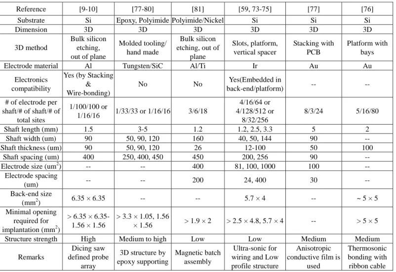
Table 1 Comparison of 3D microprobe arrays with some major design parameters
Reference [9-10] [77-80] [81] [59, 73-75] [77] [76] Substrate Si Epoxy, Polyimide Polyimide/Nickel Si Si Si Dimension 3D 3D 3D 3D 3D 3D 3D method Bulk silicon etching, out of plane Molded tooling/ hand made Bulk silicon etching, out of plane Slots, platform, vertical spacer Stacking with PCB Platform with bays Electrode material Al Tungsten/SiC Al/Ti Ir Au Au
Electronics compatibility
Yes (by Stacking & Wire-bonding) No No Yes(Embedded in back-end/platform) -- -- # of electrode per shaft/# of shaft/# of total sites 1/100/100 or 1/16/16 1/33/33 or 1/16/16 3/6/18 4/16/64 or 4/128/512 or 8/32/256 8/3/24 5/16/80 Shaft length (mm) 1.5 3-5 1.2 1.2, 2.5, 3.3 5 2
Shaft width (um) 90 50, 90, 120 160 40, 50, 144 90 -- Shaft thickness (um) 90 50, 90, 120 26 12-100 50 100
Shaft spacing (um) 400 250, 400, 450 450 200, 256 90 -- Electrode size (um2) -- -- 400 81, 100, 1000 100 --
Electrode spacing (um) -- -- 200 24, 400 30 -- Back-end size (mm2) 6.35 × 6.35 -- -- 5.7 × 4 -- ~ 5 × 5 Minimal opening required for implantation (mm2) > 6.35 × 6.35- 1.56 × 1.56 > 3.3 × 1.05, 1.56 × 1.56 > 1.9 × 2 > 2.5 × 4.8, 5.7 × 4 -- > 5 × 5 Structure strength High Medium to high Low Low Medium Medium
Remarks Dicing saw defined probe array 3D structure by epoxy supporting Magnetic batch assembly Ultra-sonic for wiring and Low profile structure Anisotropic conductive film is used Thermosonic bonding with ribbon cable
4
Method and Design
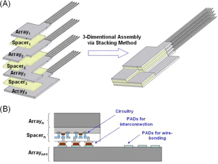
A new stacking method to produce three-dimensional neural probe arrays is presented in this work. This method creates 3-D probe arrays by assembling 2-D arrays and spacers layer by layer, as shown in Figure 1(A). For a 4 × 4 3-D array, four 2-D arrays (gray color) with four probes in each array and three spacers (yellow color) were required. Compared to exising three-dimensional neural probe designs, the present stacking method improved the inconvenient assembly steps which include orthogonal assembly and perpendicular connection techniques. In the stacking method, the shapes of each 2-D arrays were carefully designed so they can be wire-bonded individually with different height levels. Spacers with an anti-overflow mechanism were also proposed in this paper. The present anti-overflow mechanism can also be realized on 2-D arrays if active circuit chips are used as spacers. Also, the thickness of the spacer determined the spacing between two 2-D arrays. Each planar 2-D array, electrode sites, interconnect routing and bonding pads were located in the same plane. The bonding pads were arranged on the different sides of four 2-D probe arrays for wire bonding. Therefore,
each 2-D array can be wire-bonded individually and the 3-D perpendicular bonding pads used in previous work are no longer needed.
Figure 1. (A) The schematic of stacking a 4 × 4 3-D microprobe array. (B) Spacers can be
replaced by silicon substrates with signal processing circuitry for lower fabrication cost, customized design request and increases the volume usage efficiency.
By replacing spacers with active signal processing circuitry chips, the function of the 3-D neural probe array can be enhanced. For example, as shown in Figure 1(B), active circuit chips can be employed as spacers for signal processing proposes. In Figure 1(B), Spacern with active circuitry is bonded onto Arrayn+1 by the flip-chip technique, and then Arrayn is stacked onto Spacern by adhesion gel. Thus, the 3-D neural probe array
can be integrated with circuits by the present stacking method. Additionally, in IC manufacture, larger area means higher cost. When the active circuitry is fabricated with probe shafts in the back-end of the 2-D array, larger wafer areas are required. In the stacking design, spacers with circuitry and 2-D arrays were fabricated individually. Therefore, the stacking method can reduce the cost for circuitry integration and increase the design flexibility when modification of probes/circuitries is required for different applications. Besides, comparing with previous work, the volume usage efficiency was increased because there were no waste rooms between arrays and spacers. In short, the advantages of using active circuit chips as spacers include reducing the cost of circuitry integration, increasing the flexibility of the design and increasing the volume usage efficiency.
The fabrication steps of the 2-D array are briefly described as follows: (1) 250 μm-thick silicon wafer was used, and 3 μm-thick polyimide (PI) was spin-coated on the front side of the wafer for electrical isolation. (2) 1 μm-thick Cr/Au layer was electroformed and patterned for wire interconnects on the probe shaft. (3) 3 μm-thick layer polyimide (PI) was spin-coated for the interconnect encapsulation. (4) Electrode sites and wire-bonding pads were defined by DRIE. (5) 3 μm-thick Au was electroformed as electrode site and bonding pad material. Notably, the Au layer was somewhat over-electroformed to ensure that the electrode was in contact with the neural tissue while implantation. (6) The final shape of 2-D probe array was defined and released by DRIE.
The spacers were simply defined on the 250 μm-thick silicon wafer by DRIE. For different application requirements, the thickness of the 2-D arrays and spacers could be modified by using thinner wafer. However, the yield minimal wafer thickness is currently not less than 100 μm due to the accessible process limitation.
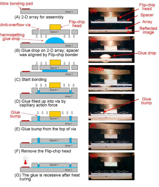
When the stacking method is used to construct the 3-D neural probe arrays, the overflow adhesion gel or glue between the stacking layers may cover the proximate bonding pads and make them ineffective. Using less gel may reduce the overflow problem, but reduce the adherent strength. To solve the overflow problem of the gel, an anti-flow mechanism design was applied in the stacking method.
The anti-overflow mechanism was accomplished by creating a through-silicon-via around the edges of the spacers. It uses capillary action force to prevent the gel from overflowing to the bonding pads. The mechanism functions in the following condition: when the stacking process starts, the combined parts compress the adhesion gel and force it to flow around. The flowing glue will fill the via by capillary action as it passes the via. Therefore, there is no redundant glue covering the proximate bonding pads
The radius of the via was one of the major design parameter in preventing overflow. The formula is given by the well-known capillary action principle [29] with definition of the liquid-air surface tension, contact angle, density of the liquid, acceleration due to gravity, the height of the liquid column and the radius of the via. In this case, the maximal height of the liquid column is the thickness of the spacer (250 μm), and the liquid-air surface tension is 0.033 N/m [30], contact angle is 70° [31], density is 2,000 kg/m3 and gravity acceleration is 9.8 m/s2. The capillary action principle gives the radius of the via a theoretical result of 4,600 μm, which was even larger than the size of the spacer. In fact, there is some limitations should be put into consideration. For instance, the limited volume of glue, the viscosity of glue, the friction force between glue-substrate interface and the capillary force in the narrow gap between two parts will make the liquid column never reach the expected height. The final via radius was experimentally set as 250 μm to enhance the filing of the via with glue.
6
Figure 2 shows the assembly parts successfully manufactured by the fabrication steps as described above. Figure 2(A) presents the fabricated parts for 3-D assembly on a one cent coin. Figure 2(B) displays the probe tip and electrode sites. Each 2-D probe array consisted of four shafts of 6 mm length, 100 μm width and the space between shafts was 110 μm. Four electrode sites were lined up on the tip along the shaft, separated by 50 μm, and the first electrode is 70 μm from the shaft tip. The circular electrode had a diameter of 20 μm and the square bonding pad had sides of length 80 μm. The tapered tip angle was around 23°. The circular via on spacers for the anti-overflow mechanism can be observed in the picture.
Figure 2. Microphotographs of fabricated 2-D arrays. (A) Fabricated parts on a one cent coin. (B)
Probe tip and electrode sites. The tapered tip angle is about 23°.
Result and Discussion
After the assembly parts were successfully fabricated, a flip-chip bonder (FINETECH Inc., USA) and thermosetting polymer (EA2151, LIONTONG Inc., TAIWAN) were used to complete the 3-D neural probe array assembly process. Convenient flip-chip technology was employed to accomplish alignment, pressurization and heating process, while the thermosetting polymer (glue) provided adhesive layer between two stacked components (array and spacer). The thermosetting glue was solidified at 185 °C in 180 s with an adhesive strength of 150–180 kg/cm3. The detailed steps to manufacture a 4 × 4 3-D neural probe array (as shown in Figure 1) using the tools as described above were as follows:
1. Array4 was fixed on the vacuum holder of the flip-chip bonder.
2. Second, adhesion gel was deposited onto the Array4 by a micro injector (MICRO FAB TECH. Inc., USA).
3. Spacer3 was picked by the flip-chip bonder head and aligned with the 2-D array by an optical microscope.
4. Then, Array4 & Spacer3 were bonded together in a pressurizing and heating condition provided by the flip-chip head.
5. After the first bonding process finished, the flip-chip head was released from the Spacer3, and then adhesion gel was deposited onto Spacer3 by the micro injector.
6. Next, Array3 was picked, aligned and bonded to the Spacer3 again.
7. Repeating the bonding process 1 to 6, we accomplished the 4 × 4 3-D neural probe array.
The maximal placement accuracy of the flip-chip was 0.5 μm in a single bonding step. Thus, the total miss-alignment error can be neglected. Moreover, the average assembly time for a 4 × 4 3-D microprobe array by manual alignment was approximately 35 minutes (including heat curing time). In the present study, we applied about 0.26 μL of gel between spacers and arrays. The appropriate amount of the adhesion get combined the stacking well without spilling to the proximate pads.
Figures 3(A)–(G) illustrate how the anti-overflow mechanism functions in the practical assembly process. The details are displayed as follows: (A) the fabricated 2-D array (Arrayn) was fixed on the flip-chip holder (not shown). (B) A drop of thermosetting polymer was deposited onto the 2-D probe array and the spacer (Spacern) was picked by the flip-chip bonder head and aligned. (C) Start bonding – the aligned spacer was moved downward and controlled by the flip-chip bonder head. After the spacer came into contact with the glue drop, the drop spread in random directions because it was squeezed by the spacer. (D) The spacer was moved continuously downward, and the glue filled the via by capillary force when it flowed past the via. (E) The spacer came into contact with the 2-D array. The gel bump occurred on the top of the via because the pressure from bonding. (F) The flip-chip bonding head was removed. (G) The assembly process was completed following thermal solidification of the thermosetting glue. The gel bump over the via rapidly receded after heat curing.
8
Figure 3 The proposed assembly anti-flow mechanism process and related practical photographs.
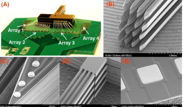
After applying the steps described in Figure 3, we successfully assembled 3-D microprobe arrays, as shown in Figure 4. Figure 4(A) displays stacked 3-D microprobe array was mounted and wire-boned onto a pre-designed PCB (~600 μm in thickness). Figure 4(B) shows a close view of 4 × 4 shafts. Figure 4(C) presents the electrodes sites at the shaft tip. Figure 4(D) illustrates the cantilever shaft structure. Figure 4(E) shows the pad for wire bonding (without wire-bonding). The electrode sites on the probe shafts were over-electroformed to ensure that the electrode can come into contact with neural tissue during implantation. Figure 4(A) also shows that the 3-D signal transmission was achieved by 2-D wire-bonding with four level of bonding pads (Array1, Array2, Array3 and Array4) in a 4 × 4 3-D arrays.
Figure 4 The photographs of successfully assembled 3-D microprobe array. (A) The wire-bonded result of
3-D microprobe array. Four different bonding levels were marked. (B) Close view of 4 × 4 shafts. (C) The electrodes sites located at the shaft tip. (D) The cantilever shaft structure. (E) Pad for wire bonding.
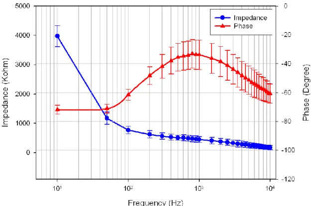
Electrode impedance spectroscopy (EIS) was used to evaluate the fabricated stacked 3-D probe arrays. The impedance characterization of 3-D neural probe array in the electrode-electrolyte interface is of utmost importance in impedance-based biosensing and neuroprotheses [32]. When the electrode sites come into contact with tissue, an electrode-tissue interface impedance was established. The electrode-tissue interface impedance and the amplifier input impedance act as a voltage divider when a neural signal passes through the electrode into the front-end amplifier. Hence, high electrode-tissue interface impedance will cause signal attenuation and induce considerable thermal noise in weak raw signal recording.
The final assembled array was characterized in physiologic saline solution (0.9% NaCl) at room temperature using a multi-frequency LCR meter (Wayne Kerr LCR meter 4235). Figure 5 presents the measured impedance of the electrodes (n =16) on the microprobe. The in-vitro impedance was 463 ± 107 kΩ and the phase was -33 degree at 1 kHz.
10
Figure 5 The electrode impedance spectroscopy of fabricated microprobe array in physiologic
saline solution. Means and standard deviations are given (n = 16).
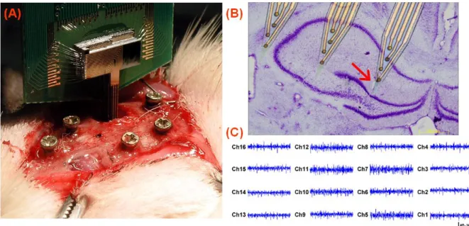
To demonstrate the practical function, the fabricated 3-D neural probe array was implanted into an anesthetized rat. Figure 6(A) shows the photograph of a stacked 3-D microprobe array that was inserted into the brain of an anesthetized rat by a manual 3-axis moving stage (not shown in the figure). The screw on the skull was adopted as a reference for measurement. The opening in the skull was about 2 mm by 3 mm. Figure 6(B) shows the photomicrograph of the implantation section. The figure was modified by superimposing a lesion marker, an implantation track, and overlaying a scaled image of the microprobe array. One lesion marker arrowhead (red) was used to identify the location of the outermost recording site, in relation to the field CA1 of the hippocampus. Figure 6(C) presents neural signals from the 16-channel microprobe array, acquired with a Multi-Channel Acquisition Processor (MAP, Plexon Inc., USA). During recordings, electrical signals were passed from the headstage to an amplifier through a band-passed filtered (spike preamp filter: 450–5 kHz, gain: 15,000–20,000) and sampled at 40 kHz per channel.
Figure 6 (A) Photograph of a stacked 3-D microprobe array inserted into the brain of an
anesthetized rat. (B) The in situ location of microprobe array was shown in the photomicrograph Nissl-stained coronal section. (C) The 16-channel neural activities simultaneously recorded from CA1 in of hippocampus.
The minimal opening is the area that must be resected, including skull and dura, to fully place an implantable device onto the brain. A smaller skull opening can reduce the implantation damage such as the rise of intracranial pressure, and the probability of wound infection. In previous work, the opening area was never less than the supporting platform [22,23] to make sure all the probes were completely inserted into tissue. Therefore, the minimal surgical opening area was defined by the supporting platform in this case. Additionally, the supporting platform area was significantly increased when ASIC chips were mounted onto the platform for system integration [2]. In the proposed stacking method, the system integration will not increase the opening area because it can be accomplished by replacing spacers with ASIC chips. The opening area of present 3-D probe array depends only on the probe array dimension. The minimum opening area of the stacked 3-D probe array is less than 1.75 mm × 1 mm, which can be readily shrunk by using thinner and narrow shafts.
Previous work may also induce additional tissue damage in the bottom of the platform as well. The interlocking structures, including tethers and joints, can cause the protrusion and damage to the tissue underneath [2]. For the stacked 3-D array, only probe array will be in contact with the target tissue.
The strength of the assembled structure is also an important issue in implantable device. Compared with the proposed 3D array, structures with tethers and joints used in previous work may not provide reliable strength to fix the probes on the platform during implantation [2,22]. The thermosetting polymer in the stacked 3-D array provided an adhesive strength of 150–180 kg/cm3 after curing. Thus, sufficiently structural strength was guaranteed in the present design.
In summary, compared with previous 3-D array studies, the advantages of using the stacking method for constructing 3-D arrays include easier assembly processes, stronger structure strength, smaller opening area and less damage to the tissue surrounding the implanting region. ASIC chips can be substituted for spacers to
12
achieve system integration without increasing device size as well. The stacking method can therefore increase the design flexibility and enhance the volume usage efficiency.
In this work, a new assembly method was applied to design a 3-D neural probe array. The fabrication and test results were also presented. The proposed stacking method can replace the vertical interconnections used in previous work with 2-D wire bonding. In this way, the supporting platform with slots and vertical spacers was no longer needed. To avoid the fluid overflow during assembly, an anti-overflow design which made use of capillary action force was applied in the stacking method as well. Furthermore, ASIC chips can also be substituted for the spacers in the stacked arrays to achieve system integration, design flexibility and volume usage efficiency. The time for manually assembling a 4 × 4 3-D microprobe array was approximately 35 minutes. Compared with previous 3-D array studies, the advantages of using the stacking method for constructing 3-D arrays include easier assembly processes, stronger structure strength, smaller opening area and less damage to the tissue surrounding the implanting region. Practical in-vivo neural spike recordings also demonstrated the functionality of the proposed neural probe array.
Reference
1. Chcurel, M. Windows on the brain. Nature 2001, 412, 266-268.
2. Yao, Y.; Gulari, M.N.; Wiler, J.A.; Wise, K.D. A microassembled low-profile three-dimensional microelectrode array for neural prosthesis applications. J. Microelectromech. Syst. 2007, 16,
977-988.
3. Frank, K.; Becker, M.C. Electrodes for extracelluar recording and stimulation. Phys. Techniques Biol. Res.
1964, 5, 22-87.
4. Green, J.D. A simple microelectrode for recording from the central nervous system. Nature 1958, 182, pp. 962.
5. Wise, K.D.; Angell, J.B.; Starr, A. An integrated-circuit approach to extracellular microelectrodes. IEEE Trans. Biomed. Eng. 1970, BME-17, 238-247.
6. Najafi, K.; Wise, K.D.; Mochizuki, T. A high-yield IC-compatible multichannel recording array. IEEE Trans. Electron Dev. 1985, 32, 1206-1211.
7. Jones, K.E.; Campbell, P.K.; Normann, R.A. A glass silicon composite intracortical electrode array. Ann. Biomed. Eng. 1992, 20, 423-437.
8. Mercanzini, A.; Cheung, K.; Buhl, D.L.; Boers, M.; Maillard, A.; Colin, P.; Bensadoun, J.C.; Bertsch, A.; Renaud, P. Demonstration of cortical recording using novel flexible polymer neural probes. Sens. Actuat. A-Phys. 2008, 143, 90-96.
9. May, G.A.; Shamma, S.A.; White, R.L. Tantalum on sapphire micro-electrode array. IEEE Trans. Electron Dev. 1979, 26, 1932-1939.
10. Wise, K.D. Silicon microsystems for neuroscience and neural prostheses. IEEE Eng. Med. Biol. Mag. 2005, 24, 22-29.
11. Drake, K.L.; Wise, K.D.; Farraye, J.; Anderson, D.J.; Bement, S.L. Performance of planar multisite microprobes in recording extracellular single-unit intracortical activity. IEEE Trans. Biomed. Eng. 1988, 35, 719-732.
12. Najafi, K.; Hetke, J.F. Strength characterization of silicon microprobes in neurophysiological tissues. IEEE Trans. Biomed. Eng. 1990, 37, 474-481.
13. Najafi, K.; Ji, J.; Wise, K.D. Scaling limitations of silicon multichannel recording probes. IEEE Trans. Biomed. Eng. 1990, 37, 1-11.
14. Paralikar, K.J.; Clement, R.S. Collagenase-aided intracortical microelectrode array insertion: Effects on insertion force and recording performance. IEEE Trans. Biomed. Eng. 2008, 55,
2258-2267.
15. Bjornsson, C.S.; Oh, S.J.; Al-Kofahi, Y.A.; Lim, Y.J.; Smith, K.L.; Turner, J.N.; De, S.; Roysam, B.; Shain, W.; Kim, S.J. Effects of insertion conditions on tissue strain and vascular damage during neuroprosthetic device insertion. J. Neural Eng. 2006, 3, 196-207.
16. Polikov, V.S.; Tresco, P.A.; Reichert, W.M. Response of brain tissue to chronically implanted neural electrodes. J. Neurosci. Meth. 2005, 148, 1-18.
17. Wise, K.D.; Sodagar, A.M.; Yao, Y.; Gulari, M.N.; Perlin, G.E.; Najafi, K. Microelectrodes, microelectronics, and implantable neural microsystems. Proc. IEEE 2008, 96, 1184-1202.
18. Campbell, P.K.; Jones, K.E.; Huber, R.J.; Horch, K.W.; Normann, R.A. A silicon-based, 3-dimensional neural interface—manufacturing process for an intracortical electrode array. IEEE Trans. Biomed. Eng.
1991, 38, 758-768.
19. Song, Y.K.; Patterson, W.R.; Bull, C.W.; Beals, J.; Hwang, N.; Deangelis, A.P.; Lay, C.; McKay, J.L.; Nurmikko, A.V.; Fellows, M.R.; Simeral, J.D.; Donoghue, J.P.; Connors, B.W. Development of a chipscale integrated microelectrode/microelectronic device for brain implantable, neuroengineering applications. IEEE Trans. Neural Syst. Rehabil. Eng. 2005, 13, 220-226.
20. Takeuchi, S.; Suzuki, T.; Mabuchi, K.; Fujita, H. 3D flexible multichannel neural probe array. J. Micromech. Microeng. 2004, 14, 104-107.
21. Hoogerwerf, A.C.; Wise, K.D. A 3-dimensional microelectrode array for chronic neural recording. IEEE Trans. Biomed. Eng. 1994, 41, 1136-1146.
22. Bai, Q.; Wise, K.D.; Anderson, D.J. A high-yield microassembly structure for three-dimensional microelectrode arrays. IEEE Trans. Biomed. Eng. 2000, 47, 281-289.
23. Bai, Q.; Wise, K.D. Single-unit neural recording with active microelectrode arrays. IEEE Trans. Biomed. Eng. 2001, 48, 911-920.
24. Herwik, S.; Kisban, S.; Aarts, A.A.A.; et al. Fabrication technology for silicon-based microprobe arrays used in acute and sub-chronic neural recording. J. Micromech. Microeng. 2009, 19,
No. 074008.
25. Du J.G.; Roukes, M.L.; Masmanidis, S.C. Dual-side and three-dimensional microelectrode arrays fabricated from ultra-thin silicon substrates. J. Micromech. Microeng. 2009, 19, No. 075008
14
26. Williams, J.C.; Rennaker, R.L.; Kipke, D.R. Long-term neural recording characteristics of wire microelectrode arrays implanted in cerebral cortex. Brain Res. Protoc. 1999, 4, 303-313.
27. Rousche, P.J.; Pellinen, D.S.; Pivin, D.P.; Williams, J.C.; Vetter, R.J.; Kipke, D.R. Flexible polyimide-based intracortical electrode arrays with bioactive capability. IEEE Trans. Biomed. Eng. 2001, 48, 361-371.
28. Takahashi, H.; Suzurikawa, J.; Nakao, M.; Mase, F.; Kaga, K. Easy-to-prepare assembly array of tungsten microelectrodes. IEEE Trans. Biomed. Eng. 2005, 52, 952-956.
29. Adamson, A.W. Physical Chemistry of Surfaces, 5th ed.; John Wiley: New York, NY, USA, 1990.
30. Cheng, C.H.; Lin, H.H. Measurement of surface tension of epoxy resins used in dispensing process for manufacturing thin film transistor-liquid crystal displays. IEEE Trans. Adv. Pack. 2008, 31, 100-106. 31. Huang, W.; Yao, Y.; Huang, Y.; Yu, Y.Z. Surface modification of epoxy resin by
polyether-polydimethylsiloxanes-polyether triblock copolymers. Polymer 2001, 42, 1763-1766.
32. Franks, W.; Schenker, W.; Schmutz, P.; Hierlemann, A. Impedance characterization and modeling of electrodes for biomedical applications. IEEE Trans. Biomed. Eng. 2005, 52, 1295-1302.
國科會補助專題研究計畫成果報告自評表
請就研究內容與原計畫相符程度、達成預期目標情況、研究成果之學術或應用價
值(簡要敘述成果所代表之意義、價值、影響或進一步發展之可能性)
、是否適
合在學術期刊發表或申請專利、主要發現或其他有關價值等,作一綜合評估。
1. 請就研究內容與原計畫相符程度、達成預期目標情況作一綜合評估
達成目標
□ 未達成目標(請說明,以 100 字為限)
□ 實驗失敗
□ 因故實驗中斷
□ 其他原因
說明:
2. 研究成果在學術期刊發表或申請專利等情形:
論文:
已發表 □未發表之文稿 □撰寫中 □無
專利:
已獲得 □申請中 □無
技轉:□已技轉 □洽談中
無
其他:
(以 100 字為限)
[1] Jin-Chern Chiou and Chih-Wei Chang,” THREE-DIMENSIONAL MICROPROBE ARRAY,” US 7946050 B2
[2] 邱俊誠、張志瑋「三維微探針陣列的組裝結構」,中華民國專利發明第 I348552 號 [3] Chih-Wei Chang and Jin-Chern Chiou, “Development of a Three Dimensional Neural Sensing
Device by a Stacking Method,” Sensors, Vol.10, no.5, pp.4238-4252, 2010. (SCI, IF=1.87) [4] C.W. Chang, Y.J. Chen, S.H. Hung and J.C. Chiou, “A WIRELESS AND BATTERYLESS
MICROSYSTEM WITH IMPLANTABLE GRID ELECTRODE/3-DIMENSIONAL PROBE ARRAY FOR ECoG AND EXTRACELLULAR NEURAL RECORDING ON RAT,” The 16th International Conference on Solid-State Sensors, Actuators and Microsystems (Transducers 2011), June 5-9, 2011, Beijing, China.
[5] Chih-Wei Chang and Jin-Chern Chiou, “Stacked Multichip Three-Dimensional Probe array toward Implantable Neural Prostheses,” The 39th Neural Interface Conference, Long Beach, CA, Jun. 21-23, 2010.
16
3. 請依學術成就、技術創新、社會影響等方面,評估研究成果之學術或應用價
值(簡要敘述成果所代表之意義、價值、影響或進一步發展之可能性)(以
500 字為限)
學術成就 此計畫衍生學術成就包括一篇國際期刊論文、獲得三個專利與數篇國際研討會論文,與此計 畫相關所訓練之碩博士約 5 名,計畫主持人也因此計畫之成果數度受邀演講相關進展。 技術創新 此計畫所開發之三維組裝技術正式將 3D IC 概念引入生醫電子元件中,成果包括兩個美國專 利與一個中華民國專利。 社會影響 此計畫延續計畫主持人先前在生醫感測器之研究,由早期體外非侵入式逐漸進入到全植入式 系統階段,可應用於癲癇病症的偵測,也與慈濟醫院進行實質的交流合作,對社會有所貢獻。 應用價值 此計畫所開發之三維探針陣列擁有與電路系統整合之能力,未來將持續專注於整合性生醫電 子產品開發,提升其實際的應用價值。國科會補助計畫衍生研發成果推廣資料表
日期: 年 月 日國科會補助計畫
計畫名稱: 計畫主持人: 計畫編號: 領域:研發成果名稱
(中文) (英文)成果歸屬機構
發明人
(創作人)
技術說明
(中文) (200-500 字) (英文)產業別
技術/產品應用範圍
技術移轉可行性及預期
效益
註:本項研發成果若尚未申請專利,請勿揭露可申請專利之主要內容。 附件三18
國科會補助專題研究計畫項下出席國際學術會議心得報告
日期: 年 月 日一、參加會議經過
二、與會心得
三、考察參觀活動(無是項活動者略)
四、建議
五、攜回資料名稱及內容
六、其他
計畫編號
NSC - - - - -
計畫名稱
出國人員
姓名
服務機構
及職稱
會議時間
年 月 日至
年 月 日
會議地點
會議名稱
(中文)
(英文)
發表論文
題目
(中文)
(英文)
附件四國科會補助專題研究計畫項下赴國外(或大陸地區)出差或研習心得報告
日期: 年 月 日一、國外(大陸)研究過程
二、研究成果
三、建議
四、其他
計畫編號
NSC - - - - -
計畫名稱
出國人員
姓名
服務機構
及職稱
出國時間
年 月 日至
年 月 日
出國地點
附件五20
國科會補助專題研究計畫項下國際合作研究計畫國外研究報告
日期: 年 月 日一、國際合作研究過程
二、研究成果
三、建議
四、其他
計畫編號
NSC - - - - -
計畫名稱
出國人員
姓名
服務機構
及職稱
合作國家
合作機構
出國時間
年 月 日至
年 月 日
出國地點
附件六國科會補助計畫衍生研發成果推廣資料表
日期:2011/11/24國科會補助計畫
計畫名稱: 子計畫一:三維電極感測陣列之研發(3/3) 計畫主持人: 邱俊誠 計畫編號: 99-2220-E-009-019- 學門領域: 晶片科技計畫--整合型學術研究 計畫無研發成果推廣資料
99 年度專題研究計畫研究成果彙整表
計畫主持人:邱俊誠 計畫編號: 99-2220-E-009-019-計畫名稱:智慧型仿生系統之晶片系統平台技術開發--子計畫一:三維電極感測陣列之研發(3/3) 量化 成果項目 實際已達成 數(被接受 或已發表) 預期總達成 數(含實際已 達成數) 本計畫實 際貢獻百 分比 單位 備 註 ( 質 化 說 明:如 數 個 計 畫 共 同 成 果、成 果 列 為 該 期 刊 之 封 面 故 事 ... 等) 期刊論文 0 0 100% 研究報告/技術報告 0 0 100% 研討會論文 0 0 100% 篇 論文著作 專書 0 0 100% 申請中件數 0 0 100% 專利 已獲得件數 1 1 100% 件 件數 0 0 100% 件 技術移轉 權利金 0 0 100% 千元 碩士生 2 2 100% 博士生 2 2 100% 博士後研究員 0 0 100% 國內 參與計畫人力 (本國籍) 專任助理 0 0 100% 人次 期刊論文 1 1 100% 研究報告/技術報告 0 0 100% 研討會論文 1 2 200% 篇 論文著作 專書 0 0 100% 章/本 申請中件數 0 0 100% 專利 已獲得件數 1 2 200% 件 件數 0 0 100% 件 技術移轉 權利金 0 0 100% 千元 碩士生 0 0 100% 博士生 0 0 100% 博士後研究員 0 0 100% 國外 參與計畫人力 (外國籍) 專任助理 0 0 100% 人次其他成果
(
無法以量化表達之成 果如辦理學術活動、獲 得獎項、重要國際合 作、研究成果國際影響 力及其他協助產業技 術發展之具體效益事 項等,請以文字敘述填 列。) 1. 成果獲邀在 2011 SEMICON TAIWAN 中展出2. 成果獲邀在 2011 SEMBA 生醫工程應用研討會中擔任 invited talk.
成果項目 量化 名稱或內容性質簡述 測驗工具(含質性與量性) 0 課程/模組 0 電腦及網路系統或工具 0 教材 0 舉辦之活動/競賽 0 研討會/工作坊 0 電子報、網站 0 科 教 處 計 畫 加 填 項 目 計畫成果推廣之參與(閱聽)人數 0
國科會補助專題研究計畫成果報告自評表
請就研究內容與原計畫相符程度、達成預期目標情況、研究成果之學術或應用價
值(簡要敘述成果所代表之意義、價值、影響或進一步發展之可能性)
、是否適
合在學術期刊發表或申請專利、主要發現或其他有關價值等,作一綜合評估。
1. 請就研究內容與原計畫相符程度、達成預期目標情況作一綜合評估
■達成目標
□未達成目標(請說明,以 100 字為限)
□實驗失敗
□因故實驗中斷
□其他原因
說明:
2. 研究成果在學術期刊發表或申請專利等情形:
論文:■已發表 □未發表之文稿 □撰寫中 □無
專利:■已獲得 □申請中 □無
技轉:□已技轉 □洽談中 ■無
其他:(以 100 字為限)
1.’ THREE-DIMENSIONAL MICROPROBE ARRAY,’ US 7946050 B2 2.「三維微探針陣列的組裝結構」,中華民國專利發明第 I348552 號 3.Sensors, Vol.10, no.5, pp.4238-4252, 2010. (SCI, IF=1.87) 4.Transducers conference, June 5-9, 2011, Beijing, China.
5.The 39th Neural Interface Conference, Long Beach, CA, Jun. 21-23, 2010.