新穎雙功函數金屬閘極製程技術之研發
137
0
0
全文
(2) 新穎雙功函數金屬閘極製程技術之研發 Investigation of Novel Dual Work Function Metal Gate Technologies Student:Tzung-Lin Li Advisor:Dr. Chun-Yen Chang. 研究生:李宗霖 指導教授:張俊彥 博士. 國立交通大學 電子工程學系 電子研究所 博士論文. A Dissertation Submitted to Department of Electronics Engineering and Institute of Electronics College of Electrical and Computer Engineering National Chiao Tung University In Partial Fulfillment of the Requirements For the Degree of Doctor of Philosophy in Electronics Engineering June 2006 Hsinchu, Taiwan, Republic of China. 中 華 民 國 九 十 五 年 六 月.
(3) 新穎雙功函數金屬閘極製程技術之研發 研究生:李宗霖. 指導教授:張俊彥 博士. 國 立 交 通 大 學 電子工程學系 電子研究所 博士論文. 摘要. 本論文的研究方向,主要為研發新穎之雙功函數金屬閘極製程技 術。元件尺寸的微縮雖可以改善元件之操作特性,然而傳統的多晶矽 閘極本質上的缺點,對元件特性的負面影響也將更加顯著。另一方 面,隨著元件尺寸的微縮,閘極氧化層的厚度變薄也將導致閘極漏電 流大幅上揚,為了有效降低閘極漏電流,近年來以高介電材質取代傳 統二氧化矽的相關研究也被投注大量心力。然而多晶矽閘極搭配高介 電材質,已被發現會有熱穩定性不佳的缺點,同時介面也存在著費米 能階夾止效應,因此,金屬閘極製程的研發不僅可以克服上述多晶矽 的本質缺點,對於與高介電材質間的熱穩定性、費米能階夾止效應等 方面,也提供了可能的解答。此外,金屬閘極的低阻抗,對於元件的 高頻操作特性亦有改善之效。 對於金屬閘極的製程技術與材料選擇有以下幾項基本要求,首先 它必須能夠在閘極介電層介面提供正確適當的功函數值,同時與閘極. i.
(4) 介電層間需有良好的熱穩定性以確保在元件製程中可以保有穩定的 特性,另外也必須可相容、整合於傳統的製程技術中。本論文中,我 們提出了兩種新穎的雙功函數金屬閘極製程技術,一是利用金屬混合 以形成雙元合金,二是以金屬矽化反應以形成金屬矽化物。應用了此 等金屬功函數調變法後,早期被提出的雙功函數金屬閘極製程技術 中,閘極介電層因金屬蝕刻導致厚度的不均勻性以及可靠度退化的現 象將可被避免。在雙元合金的實驗中,我們先以同時性濺鍍的物理沈 積法沈積鉿鉬雙元合金,藉以觀察其電性、化性。藉由改變各靶材的 濺鍍功率可調變鉿鉬合金的組成,進而得到近乎線性且連續的功函數 調變,其調變範圍可介於 3.93eV(純金屬鉿)與 4.93eV(純金屬鉬) 之間。我們也發現鉿鉬合金在二氧化矽上的熱穩定性,雖然會隨著鉿 含量的增加而變差,但至少都可達 400℃以上。 基於製程整合上的考量,我們進一步驗證了沈積鉿、鉬兩金屬層 並經熱處理使其混合的方式以形成鉿鉬雙元合金,並藉此提出一雙功 函數金屬閘極製程技術。由於達到完全的金屬混合以形成雙元合金所 需的熱預算取決於兩金屬層的厚度總和 TM (TM = THf + TMo),我們提 出了一個概念:根據金屬沈積後製程所需經過的總熱處理預算,選用 適當的金屬層總厚度,則可以避免掉對金屬閘極材質本身熱穩定性的 要求。此外,我們也驗證了藉由改變鉿、鉬兩金屬層的厚度比例 TR (TR = THf / TMo),可以精確地控制所形成的雙元合金的組成以及功函數 值 。 上 述 的 技 術 對 於 具 有 先 進 結 構 的 元 件 諸 如 : FinFET 、 UTB-MOSFET 將相當具有吸引力,因為先進元件通常具有較薄的基 板厚度,且基板的雜質摻雜濃度對元件臨界電壓的調變效果也大幅降 低。此外,先進元件所需的閘極功函數值會隨基板厚度與閘極數目的 ii.
(5) 不同而有所差異,因此準確的功函數調變將會益形重要。 論文中所提出的第二種雙功函數金屬閘極製程技術則是應用了 金屬的矽化反應。我們選擇在具有良好熱穩定性的金屬鉬上沈積了適 當厚度的非晶矽,再藉由熱處理過程使其經由矽化反應生成矽化鉬, 並藉此提出使用金屬鉬與矽化鉬作為閘極組合的雙功函數金屬閘極 製程技術。在二氧化矽上,金屬鉬-矽化鉬之閘極組合所提供的功函 數組合可適用於具有先進結構的元件,且矽化鉬亦被驗證具有良好的 熱穩定性。另外我們發現在矽化反應之前,如果於非晶矽中佈植摻雜 入雜質砷,則可進一步降低所生成矽化鉬的功函數值,進而拉大金屬 鉬-矽化鉬之間的功函數差,將所提出的雙功函數金屬閘極製程技術 之應用範圍擴大到傳統的本體元件。值得一提的是,此提出的新穎製 程技術是利用金屬本身搭配本質或 n 型金屬矽化物來提供功函數 差,有別於近期被廣泛研究的 FUSI 技術中利用 p 型與 n 型金屬矽化 物來提供功函數差。由於避免了 p 型金屬矽化物的使用,因此可以消 除硼穿透可能帶來的缺點。 我們同時也驗證了金屬鉬-矽化鉬之閘極組合在高介電材質上的 特性。我們發現金屬鉬與矽化鉬在二氧化鉿的高介電閘極介電層上所 得到的功函數值都分別略低於在二氧化矽上所得到的值,然而兩者間 的功函數差值卻可維持。同時,矽化反應之前,於非晶矽中雜質砷的 佈植仍然可以有效降低所形成矽化鉬在二氧化鉿上的功函數值,克服 了 FUSI 技術在二氧化鉿高介電閘極介電層上,p 型與 n 型金屬矽化 物幾乎無功函數差的致命缺點。相較於 FUSI 技術,雖然同樣運用到 金屬的矽化反應,然而我們的實驗結果卻顯示出費米能階夾止效應被 iii.
(6) 有效壓抑。對此我們猜測其原因是:我們所提出的金屬鉬-矽化鉬雙 功函數金屬閘極製程技術,其結構有效避免了非晶矽層在沈積過程以 及矽化反應之前與高介電閘極介電層的直接接觸。. iv.
(7) Investigation of Novel Dual Work Function Metal Gate Technologies Student : Tzung-Lin Li. Advisor : Dr. Chun-Yen Chang. Department of Electronics Engineering & Institute of Electronics National Chiao Tung University. Abstract Two novel dual work function metal gate technologies are investigated and proposed. With the down-scaling of the device geometry for performance improvement, inherent drawbacks of conventional polysilicon gate electrodes lead to increasingly significant negative influence. In addition, the high-k gate dielectrics have been introduced to replace the conventional silicon dioxide. Consequently, under the same effective oxide thickness, the gate leakage current can be effectively reduced. Unfortunately, polysilicon gates have been reported to be thermodynamically unstable on many high-k materials and lead to Fermi-level pinning effect at the polysilicon/high-k interface. Therefore, metal gates are expected to provide a turning point in possessing a better thermal stability and a retardation of the Fermi-level pinning effect. In addition, metal gates can possess a lower gate resistance and enhance the device performance at higher frequency.. The basic requirements for a novel metal gate technology include providing v.
(8) suitable work function values at the gate dielectric interface, the good enough thermal stability with the underlying gate dielectrics and a compatible device integration process. Two novel metal gate technologies are proposed in this dissertation. One is based on the metal intermixing technique, and the other is based on the silicidation technique. We firstly investigate the electrical and chemical characteristics of Hf-Mo binary alloys deposited by co-sputtering technique. A continuous and almost linear work function adjustment using HfxMo(1-x) is demonstrated for the first time. The work function value of Hf-Mo binary alloy ranges from 3.93eV (Φm of pure Hf) to 4.93eV (Φm of pure Mo) and depends on the sputtering power ratio of each target. The thermal stabilities of Hf-Mo binary alloy on SiO2 are found to degrade with the increase of Hf atomic fraction, but all of the Hf-Mo binary alloys possess thermal stabilities at least higher than 400℃. The Hf-Mo binary alloys can be appropriate for a gate-last SiO2 CMOS process.. The practicable integration of Hf-Mo binary alloys into the dual metal gate process is also proposed. HfxMo(1-x) formed by metal intermixing of the Hf/Mo stack is firstly evaluated, and a novel dual work function metal gate technology is then proposed and demonstrated. A precise control over the work function of the Hf-Mo binary alloy by adjusting the composite metal thickness ratio TR (TR = THf / TMo) is demonstrated. Besides, the required thermal budget for a complete metal intermixing is demonstrated to depend on the total metal thickness, TM (TM = THf + TMo). Therefore, one can be allowed to get around the thermal stability issue by using an appropriate TM value. This technique is not only attractive but especially important for devices with advanced transistor structures, such as FinFET and/or UTB-MOSFET devices, since the substrate doping modulation may not be an efficient way to adjust the threshold voltages of devices with advanced transistor structures. vi.
(9) The other novel dual metal gate technology proposed in this dissertation is based on using the silicidation technique. The α-Si/Mo stack was fabricated and thermal annealed to form MoSix. The work function of MoSix is found to be lower than that of Mo, and the thermal stability of MoSix is evaluated to be higher than 950℃. Combining MoSix with the pure Mo gate, a practical integration into the dual metal gate technology is then proposed. On the SiO2 gate dielectric, the combination of Mo-MoSix possesses a work function shift appropriate for devices with advanced transistor structures. Furthermore, the additional arsenic pre-implantation into the. α-Si layer prior to the silicidation annealing is demonstrated to effectively lower the work function of MoSix. Consequently, the application of the proposed novel dual metal gate technology can be expanded to the conventional bulk devices. Besides, the new structure along with the ruling out of p-type metal silicide is also demonstrated to eliminate the boron penetration problem encountered with the reported FUSI method.. On high-k gate dielectric materials, the maintenance of the considerable work function shift is also demonstrated. The extracted Φm value of pure Mo or MoSi2 gate on HfO2 is slightly lower than that on SiO2, but the Φm difference between Mo and MoSix is almost the same regardless of the underlying gate dielectric materials. The arsenic pre-implantation still has effect upon the modulation of Φm of metal silicide on HfO2, even though the modulation range is a little smaller than that on SiO2. The influence of Fermi-level pinning effect, which has been reported to be responsible for the high threshold voltages of FUSI gated devices with the high-k gate dielectric, is also discussed. The Fermi-level pinning effect seems to be retarded in the proposed Mo-MoSix dual metal gate technology. We speculate that the improvement may be attributed to the separation of silicon layer from the high-k gate dielectrics.. vii.
(10) 誌. 謝. 論文完成的同時,心中實是百感交集,感恩之心不曾少過。首先, 我要感謝一直支持、鼓勵我的指導教授. 張俊彥校長,自碩士班起就. 接受老師的研究指導,轉眼已有八年之久。老師除了在專業學術領域 上的創新遠見令我受益無窮外,不忮不求的風範也讓身為學生的我深 表欽佩,科技與人文並重的學風、國際級學者的氣度,也對我產生潛 移默化的影響,能有幸跟隨老師研究,我想是我人生中最重要的轉捩 點。 同時要感謝台灣積體電路製造公司的. 胡正明教授。胡教授在半. 導體領域上的成就與造詣亦是國際馳名的,很感謝胡教授在研究方向 上所提供的建議、支援與討論,讓碩士班時研究射頻電路設計,而在 博士班轉換研究領域的我能不感到徬徨。另外也要感謝台灣積體電路 製造公司的. 王志豪博士,感謝他在繁忙的工作之餘,仍能全力提供. 我所需的幫助與支持。 另外謝謝我的直屬學弟:胡嘉欣、何武陵、陳弘斌、謝彥廷,很 高興有機會與各位合作研究,教學相長的過程也讓我獲益良多,希望 各位都能繼續努力,在自己的工作領域或研究成果上能有所突破。 當然還要感謝快速電子實驗室的所有成員,有你們的陪伴與相互 扶持,讓我的研究生活增添了許多的歡樂與色彩。尤其是陳經緯博 士、彭辭修博士、黃啟環學弟,在我轉換研究領域時,他們的幫助與 扶持,讓我走得更為平順。也感謝吳師道博士、彭杜仁博士、楊宗熺 博士、以及各位學弟妹們:羅文政、陳漢譽、黃聖懿、涂峻豪、胡心 viii.
(11) 卉、鄭兆欽、馮立偉、陳怡誠、陳緯仁、余昱穎、林哲弘、劉峻丞、 張哲榮、邵而康、沈詩國,還有許多已經畢業分飛的 418 成員、好友 陳舒薇、張瑋怡以及其他關心我的人,有你們的陪伴讓我的求學過程 更值得回憶。 八年前隻身來到新竹求學,如今謹將這份成果獻給我最愛的家 人,感謝爸媽含辛茹苦的扶養、支持、鼓勵與諒解,讓我毫無後顧之 憂得以順利完成博士論文;也感謝女友伊喬六年來在感情與生活上的 相伴照顧、包容體諒,陪我度過生活中的悲喜、生命中的起伏。因為 你們,我的人生變得更完美,成就也變得更有意義。. 李宗霖 誌於. 風城交大 2006. ix.
(12) Contents Abstract (Chinese). i. Abstract (English). v. Acknowledgement. viii. Contents. x. Table Captions. xiii. Figure Captions. xiv. Chapter 1. Introduction. 1.1. Evolution of Gate Electrode Candidates. 1. 1.2. Basic Requirements for Metal Gates. 4. 1.3. Metal Work Function Extraction Technique. 6. 1.4. Organization of the Thesis. 8. References. Chapter 2. 11. Investigation of HfxMo(1-x) Binary Alloys. 2.1. Backgrounds and Motivation. 23. 2.2. Experiment. 25. 2.3. Results and Discussion. 26. 2.4. Summary. 29. References. 30. Chapter 3. Integratable. Dual. Metal. HfxMo(1-x) Binary Alloys x. Gate. Technology. Using.
(13) 3.1. Backgrounds and Motivation. 46. 3.2. Experiment. 47. 3.3. Results and Discussion. 48. 3.4. Summary. 51. References. 52. Chapter 4. Novel Dual Metal Gate Technology Using MoSix Films. 4.1. Backgrounds and Motivation. 62. 4.2. Experiment. 64. 4.3. Results and Discussion. 66. 4.4. Summary. 70. References. 72. Chapter 5. Investigation. of. MoSix. Based. Dual. Metal. Gate. Technology on the High-k Gate Dielectric 5.1. Backgrounds and Motivation. 96. 5.2. Experiment. 99. 5.3. Results and Discussion. 99. 5.4. Summary. 101. References. 102. Chapter 6. Conclusions and Suggestions for Future Work. 6.1. Contributions of the Study. 111. 6.2. Suggestions for Future Work. 113 xi.
(14) Vita (Chinese) Publication List. xii.
(15) Table Captions Chapter 2 Table 2.1. Sample conditions and extracted Φm of co-sputtering experiment. (alloy samples : 400℃, 30s;control samples : as-deposited). Chapter 3 Table 3.1. Sample conditions and extracted Φm of metal intermixing experiment. (700℃, 30s for sample 2-1 and 2-2;600℃, 30s for samples 2-3 and 2-4). xiii.
(16) Figure Captions Chapter 1 Fig. 1.1. Illustration of gate misalignment.. Fig. 1.2. Illustration of self-aligned process.. Fig. 1.3. Illustration of polysilicon gate technology using only n+-poly for both n- and p-channel devices.. Fig. 1.4. Illustration of dual-doped polysilicon gate technology.. Fig. 1.5. Illustration of the boron penetration.. Fig. 1.6. Illustration of the poly depletion effect.. Chapter 2 Fig. 2.1. C-V curves of as-deposited co-sputtering samples. Wide-ranging flat band voltage shift can be observed.. Fig. 2.2. All samples (Table I.) exhibited linear behavior in VFB vs. EOT curves from which work function of each alloy could be extracted. (alloy samples : 400℃, 30s;control samples : as-deposited). Fig. 2.3. The as-deposited pure Mo film is found to have (110) orientation.. Fig. 2.4. Process quality was demonstrated, since the 50% Hf power ratio sample suffering maximum power summation during metal deposition still exhibited negligible hysteresis.. Fig. 2.5. C-V curve of post-400 ℃ annealing Hf gated capacitor shows noticeable EOT variation and flatband voltage shift.. Fig. 2.6. Post-400℃ annealing co-sputtering sample shows negligible work. xiv.
(17) function variation. Fig. 2.7. The dependence of Φm and EOT variation on annealing temperature show that the thermal stability of alloy samples can be at least higher than 400℃.. Fig. 2.8. Calculated work function value versus atomic fraction in binary alloy as a function of γ ratio. Metals with similar γ (Sommerfeld factor) will lead to a linear work function modulation which is a compromise between modulation efficiency and immunity to process variation. (Φm.A and Φm.B are set to be 3.93 and 4.93eV for convenience). Fig. 2.9. The phase diagram of Mo-Hf system.. Fig. 2.10. Comparison between experimental (Table I.) and theoretical work function values. A slightly deviation in lower Hf power ratio regime may be attributed to different sputtering rate between Hf and Mo. (γHf = 2.16, γMo = 2.0 are used for calculation). Fig. 2.11. XRD spectra of 50% Hf power ratio co-sputtering sample exhibited an amorphous film structure and only the c-Si was featuring.. Fig. 2.12. AES profile of post-annealing 50% Hf power ratio co-sputtering sample. A uniform composition and abrupt interface can be observed.. Chapter 3 Fig. 3.1. Schematics of dual metal gate technology using metal and alloy formed by metal intermixing. Metals need not to be etched away from the dielectric surface so the uniformity and integrity of gate dielectric can be preserved.. Fig. 3.2. C-V curves of Hf-295Å/Mo-205Å/SiO2 capacitor before and after xv.
(18) thermal annealing. The optimal annealing temperature for this sample was found to be 600℃. Fig. 3.3. The increase of total metal thickness under the same composite metal thickness ratio can effectively rise the optimal annealing temperature.. Fig. 3.4. Illustration of thinning down of the gate electrode using ILD CMP.. Fig. 3.5. C-V curves of post-annealing Hf/Mo/SiO2 capacitors as a function of Hf atomic fraction.. Fig. 3.6. Comparison between experimental (Table II.) and theoretical results. A parallel shift may be attributed to the extra Hf consumption (~3%) due to surface oxidation. Also shown as open symbols are experimental results of multilayer (TiN/Mo/Hf/Mo) gated devices, good agreement on theoretical results can be achieved.. Fig. 3.7. XRD spectra of metal intermixing sample (Hf-206Å/Mo-294Å/SiO2) exhibited HfO2 peak as a result of oxidation of Hf at the top surface after thermal treatment.. Fig. 3.8. Post-annealing work functions extracted from two-layer (Hf/Mo) and multilayer (TiN/Mo/Hf/Mo) gated MOSCAP versus the composite metal thickness ratio (TR = THf / TMo). Also shown are calculated results of derived quadratic equations with and without taking extra Hf consumption into account.. Chapter 4 Fig. 4.1. The schematic illustration of dual metal gate technology gated by the combination of different metal silicides.. Fig. 4.2. The schematic illustration of the reported dual metal gate technology xvi.
(19) using FUSI method. Fig. 4.3. The schematic illustration of the proposed novel dual metal gate technology gated by the combination of metal and metal silicide.. Fig. 4.4. The practical integration of the proposed novel dual metal gate technology gated by the combination of metal (Mo) and metal silicide (MoSix).. Fig. 4.5. Capacitance-voltage curves of post-silicidation α-Si/Mo/SiO2/p-Si MOSCAP as a function of the thickness of α-Si.. Fig. 4.6. Capacitance-voltage. characteristics. of. MOSCAP devices. with. α-Si/Mo/SiO2/n-Si structure before and after silicidation annealing. Fig. 4.7. The VFB versus EOT plots of Mo and MoSix gated MOSCAP devices before and after 950℃ RTA for thermal stability evaluation.. Fig. 4.8. The dependence of the EOT variation on annealing conditions for MOSCAP devices with Mo/SiO2/n-Si structure.. Fig. 4.9. The dependence of the extracted work function value on annealing condition for MOSCAP devices with Mo/SiO2/n-Si structure.. Fig. 4.10. The dependence of the EOT variation on annealing conditions for MOSCAP devices with α-Si/Mo/SiO2/n-Si structure.. Fig. 4.11. The dependence of the extracted work function value on annealing temperature for MOSCAP devices withg α-Si/Mo/SiO2/n-Si structure.. Fig. 4.12. The TDDB lifetime projection of the Mo/SiO2 device. Superior TDDB characteristic for pure Mo gate annealed by 950℃ RTA for 30s is demonstrated.. Fig. 4.13. The TDDB lifetime projection of the post-silicidation α-Si/Mo/SiO2 device. Superior TDDB characteristic for MoSix gate annealed by 950 ℃ RTA for 30s is demonstrated. xvii.
(20) Fig. 4.14. The accumulation leakage current densities of Mo/SiO2/n-Si and MoSix/SiO2/n-Si devices annealed by 950℃ for 30s.. Fig. 4.15. Work function extraction of MoSi2 on SiO2. In this case, the MoSi2 is sputtering-deposited using the MoSi2 target.. Fig. 4.16. The x-ray photoelectron spectroscopy (XPS) analysis shows that the binding energy corresponding to the Si 2p spectra of silicided films is 0.4eV lower than that of pure Si.. Fig. 4.17. The x-ray photoelectron spectroscopy (XPS) analysis shows that the binding energy corresponding to the Mo 3d spectra of silicided films is 0.2eV lower than that of pure Mo.. Fig. 4.18. The VFB versus EOT plots of post-silicidation α-Si/Mo gated MOSCAP. devices. with. (5x1015cm-2). and. without. arsenic. pre-implantation dosage. Fig. 4.19. The dependence of Φm values on the doses of arsenic pre-implantation.. Fig. 4.20. The dependence of the EOT variation on annealing conditions for MOSCAP devices with α-Si/Mo/SiO2/n-Si structure with 5x1015 cm-2 arsenic pre-implantation.. Fig. 4.21. The dependence of the extracted work function value on annealing conditions for MOSCAP devices with α-Si/Mo/SiO2/n-Si structure with 5x1015 cm-2 arsenic pre-implantation.. Chapter 5 Fig. 5.1. The schematic illustration of dual metal gate technology gated by the combination of polysilicon and metal silicide.. Fig. 5.2. The capacitance-voltage characteristics of MOSCAP devices with xviii.
(21) α-Si/Mo/HfO2/n-Si structure before and after silicidation annealing. Fig. 5.3. The capacitance-voltage characteristics of pure Mo gated MOSCAP devices on the HfO2 gate dielectric after RTA at 950℃ for 30s.. Fig. 5.4. The dependence of Φm values on gate dielectric materials for pure Mo and MoSix gate electrodes.. Fig. 5.5. The dependence of Φm values on gate dielectric materials for MoSix gate electrodes with and without arsenic pre-implantation.. Fig. 5.6. Schematic explanation of the machenism of Fermi-level pinning effect relaxation in the proposed novel approach.. xix.
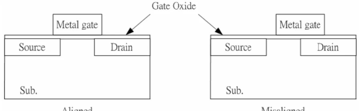
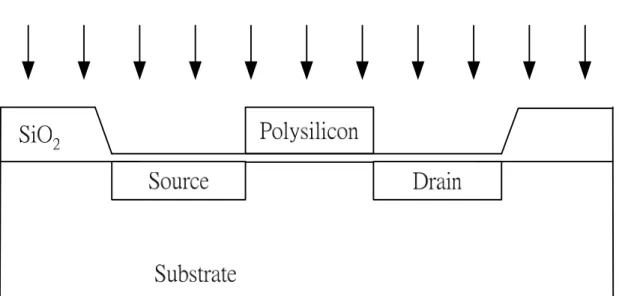
(22) Chapter 1. Introduction. 1.1 EVOLUTION OF GATE ELECTRODE CANDIDATES Before the mid-1970s, the doping technique was accomplished by the diffusion process in high-temperature furnaces. After the source/drain (S/D) diffusion, the thin gate oxide is grown and the metal gate is deposited. If the gate mask is misaligned with the S/D mask, the transistor will not work properly as shown in fig. 1.1. Oversized gate electrodes are required to ensure the complete gate coverage over the S/D. The gate misalignment issue leads to a great challenge especially when devices are scaled down.. The application of ion implantation solved the gate alignment problem by using the so-called self-aligned S/D doping process as shown in fig. 1.2. In this case, the gate oxide is grown followed with the deposition, patterning, and etching of gate electrodes. The ion implantation is used to form the S/D region and a high temperature annealing process is required to repair the damage due to the implantation process and to activate the implanted dopant. Since the required annealing temperature is usually higher than the melting point of aluminum (Al), a different gate electrode candidate has to be introduced. Polysilicon and silicide/polysilicon stack (polycide) have been used as the gate materials for several device generations. 1.
(23) In the late-1980s, the need to reduce the power consumption of the integrated circuit (IC) was one of the major driving forces for complementary MOS (CMOS) devices development. Early CMOS based ICs used n+-polysilicon as gate electrodes for both n-MOS and p-MOS devices as shown in fig. 1.3. To suppress the punch through in p-MOS devices, the substrate doping concentration will need to be increased. Along with the use of lower Fermi energy n+-polysilicon as gate electrode, the threshold voltage of p-MOS will be too negative to be acceptable. A thin sheet of negative charges must therefore be placed at the Si/SiO2 interface in p-MOS devices. This can be accomplished by implanting a shallow layer of boron atoms. The boron dose must be heavy enough to compensate the n-surface so that a thin p-region is formed and shifts the threshold voltage of p-MOS toward more positive value. However, this technology (n+-polysilicon for both n-MOS and p-MOS) will lead to a buried-channel p-MOS device which will exhibit enhanced susceptibility to short-channel effects. Solutions involving the use of gate electrodes other than n+-polysilicon must therefore be explored. One alternative is to use n+-polysilicon and p+-polysilicon for n-MOS and p-MOS devices, respectively, as shown in fig. 1.4. Such a so-called dual-doped poly approach, however, introduces other problems. One drawback is the poor threshold voltage control in the p-MOS devices due to penetration of the boron atoms into the oxide or further into the silicon substrate, as shown in fig. 1.5, especially when a thin gate oxide is used [1]. It has also been found that the presence of fluorine in the gate oxide worsens the boron penetration problem [2, 3]. Such fluorine can be introduced into the gate oxide if the p-MOS S/D regions are formed using BF2 implantation which is suggested for shallow junction formation.. Another problem encountered with conventional polysilicon gates is the. 2.
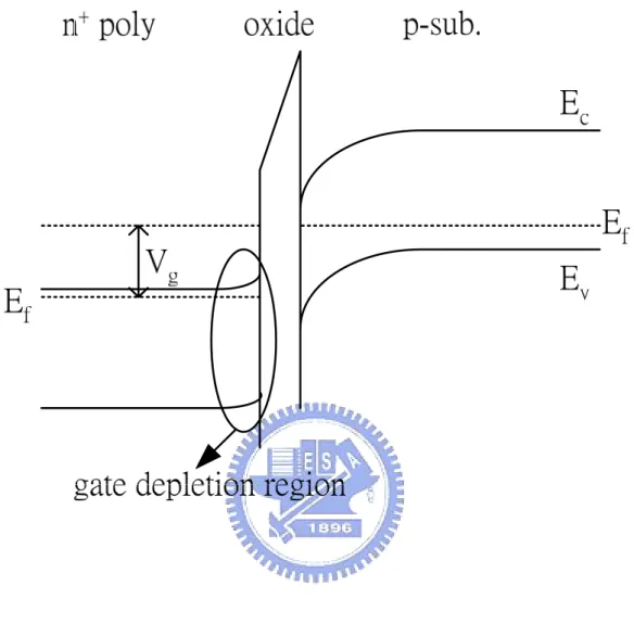
(24) so-called poly depletion effect as shown in fig. 1.6 [4]. If the polysilicon gate is not doped heavily enough, problems will arise from the depletion of the gate itself. Gate depletion results in an additional capacitance in series with the gate oxide capacitance, which in turn leads to a reduced inversion-layer charge density and degradation of the MOSFET transconductance. It is worth to note that the boron penetration and poly depletion effect in p-MOS devices will influence each other. Heavily boron concentration is needed for p+-polysilicon to suppress the poly depletion effect in PMOS while it potentially makes the boron penetration problem more pronounced.. It is also worth to note that the shrinkage of oxide thickness can improve the device short channel performance, however, the increasing leakage current leads to the noticeable standby power. Replacing the conventional silicon dioxide gate stack with the novel high-k gate dielectric material draws more and more attention in the last several years. The use of the high-k gate dielectric can possesses larger physical oxide thickness under the same electrical oxide thickness and results in effective leakage current reduction. Several high-k materials have been investigated as new gate dielectric candidates such as TiO2, Ta2O3, Al2O3, ZrO2, HfO2, La2O3, Y2O3 and Pr2O3. Among these candidates, HfO2 not only has relatively high dielectric constant and bandgap but also exhibits the impressive thermal stability with the silicon substrate. The polysilicon/HfO2 interface, however, will lead to the so-called Fermi-level pinning effect which is believed to have been caused by Si-Hf interaction and leads to high threshold voltages of MOSFET devices. Moreover, polysilicon gates are found to be thermodynamically unstable on many high-k materials [5, 6] so that metals are expected to provide a turning point in possessing a better thermal stability.. 3.
(25) 1.2 BASIC REQUIREMENTS FOR METAL GATES The use of metal/high-k structure, however, will introduce several new challenges such as the choice of metal candidates, the development of a compatible process and the thermal stability issue between metal and high-k gate dielectric.. The work function value of the introduced metal candidate will significantly influence threshold voltages of fabricated devices. High performance CMOS technology generally requires two separate gate work function values for n-MOS and p-MOS devices. Providing appropriate work function values at the gate dielectric interface, one can achieve low and symmetric threshold voltages for n- and p-channel devices without high dosage channel implantation which potentially leads to the threshold voltage non-uniformity and the carrier mobility degradation. Metals with midgap work function, such as W and TiN, have been firstly adopted as gate candidates for symmetric threshold voltage values. However, the magnitude of resulted threshold voltages for both n- and p-channel devices would be too large to be acceptable [7, 8]. To avoid applying heavily counter channel doping, the dual work function metal gate technology has been proposed [9-11]. The major concept is similar to the dual-doped polysilicon technology where different gate materials with suitable work function values are served as gate candidates for n- and p-channel devices. The chosen metal candidates should provide suitable work function (Φm) values at the dielectric interface. For instance, metal gates should possess work function values of about 4eV and 5eV to replace the conventional n+- and p+-polysilicon gates, respectively, for surface-channel bulk devices. Moreover, several. 4.
(26) advanced devices with new transistor structures, such as FinFET and ultra-thin-body (UTB) MOSFET, have been developed recently [12-19]. These advanced devices have better gate-to-channel controllability. Consequently, the required gate work function values for low and symmetric threshold voltages will be different from those in bulk devices. Moreover, the adjustment of the substrate doping is no longer an effective way of threshold voltage control in advanced devices. Choosing metal gate candidates with suitable work function values becomes a more and more importance topic. The reported simulation results show that the required gate work function for nand p-channel advanced devices are about 4.4~4.6eV and 4.8~5.0eV, respectively.. In addition, the chosen metal candidates should be able to possess good thermal stability with the underlying gate dielectric material. Consequently, the undesired interaction at metal/gate dielectric interface during the device fabrication process can be avoided, and the process induced Φm and/or the equivalent oxide thickness (EOT) variations can be suppressed. Although the recently developed gate-last (also called replacement gate) technique can provide a new chance of using low thermal stable materials as gate electrodes [20-26], the fabrication process will become more complex and lead to new challenges such as dummy gate removal and metal polish.. The development of suitable process integration is also an important issue to avoid the possible process-induced performance degradation. Several metal gate technologies have been widely investigated in the last decade. The firstly proposed dual work function metal gate technology exhibits a straightforward fabrication process [9, 10]. Although the used Ti and Mo have suitable work function values for n- and p-channel devices, respectively, the proposed integration process inherently makes the gate dielectric material exposed to the metal etchant and leads to an. 5.
(27) undesired reliability problem and oxide thickness non-uniformity.. To overcome this phenomenon, a novel dual work function metal gate technology using Ni-Ti interdiffusion has been proposed [27, 28]. Although this approach is quite material-dependent, it provides a lot of suggestions and recommendations on the dual metal gate technologies. Furthermore, a novel metal work function adjustment technique using nitrogen implantation has been proposed [29-32]. This approach is good at the ease of process integration but the modulated range of work function may not be large enough and the process stability will be a challenge.. Recently, a so-called fully silicidation (FUSI) method has been proposed to apply for implement of dual work function metal gate technology [33-38]. The front-end process is the same with the traditional dual-doped polysilicon gates CMOS technology while the conventional salicide process is modified. A metal layer thicker than that required for conventional salicide process is required to allow for full silicidation of the existed polysilicon gates. And dopants in the polysilicon are demonstrated to be able to modify the work function value of the formed metal silicide (MeSi) gates.. Several metal candidates, metal nitrides and binary alloys have also been widely investigated in the last five years. To sum up, the dual work function metal gate technology is drawing more and more attention.. 1.3 METAL WORK FUNCTION EXTRACTION TECHNIQUE 6.
(28) There are several methods for the metal gate work function extraction. One is comparing the flat-band voltage shift of MOSCAP devices between the under test metal gate electrode and that with known work function value such as n+ poly-silicon. In this case, devices should be subjected to the similar process flow and the same thermal budget. From the known work function of n+ poly-silicon and flat-band voltage difference between n+ poly-silicon and the under test metal, the metal work function can be estimated. But the value of the extracted metal work function in this approach would be less precise due to the different gate electrode deposition processes for polysilicon and metal gates. In general, metal gates are deposited using sputtering system, and this physical vapor deposition (PVD) system will inherently result in more oxide charges contributing to flat-band voltage difference.. Another approach bases on the expression of the flat-band voltage in a MOS system [29]:. VFB = Φ ms −. Qf Q = Φ ms − f tox Cox ε ox. (1.1). where Qf is the density of fixed charges in the oxide, εox is the permittivity of the dielectric material and tox is the thickness of the gate dielectric. To decouple the effect of fixed oxide charges, Capacitance-voltage measurements of MOSCAP devices with different oxide thicknesses will be performed to generate the flat-band voltage (VFB) versus the effective oxide thickness (EOT) plot. The intercept of VFB axis corresponds to the value of Φms. The value of Φs can be calculated according to the information of the electron affinity of silicon substrate, silicon energy bandgap and the potential difference between the intrinsic and doped silicon Fermi level. Work function values obtained in this way, however, would be fair approximations after accounting for. 7.
(29) uncertainties in flat-band voltage determination and the contributions of interface trap state.. Notably, it has been reported that the quantum mechanical (QM) effect becomes significant in the oxide thickness extraction as oxide thickness is reduced [39, 40]. Carrier transporting in the channel is confined by a triangular energy well. Consequently, the charge centroid locates further from the surface than that predicted by the classic analysis. This quantum mechanical effect will contribute additional effective oxide thickness and then lead to a deviation in metal work function extraction. Several capacitor-voltage simulators with the consideration of quantum confinement effect, such as QMCV and NCSU-CV, have been proposed. In this thesis, we use the QMCV simulator established by UC Berkeley Device Group for the determinations of the flat-band voltage and effective oxide thickness.. 1.4 ORGANIZATION OF THE THESIS Two novel dual-work function metal gate technologies are proposed and investigated in this dissertation. First, the dual metal gate technology based on the use of Hf-Mo binary alloys is demonstrated. Second, the silicidation technique is used to implement a dual metal gate technology with metal-metal silicide combination.. In chapter 1, an introduction to the gate candidate evolution and a brief review of state-of-the-art metal gate technologies are discussed. Basic requirements of novel metal candidates are also addressed. Moreover, the used work function extraction technique in this dissertation is also mentioned. 8.
(30) In chapter 2, the electrical and chemical characteristics of Hf-Mo binary alloys are investigated. The continuous and almost linear work function adjustment using HfxMo(1-x) is demonstrated for the first time. The work function value of Hf-Mo binary alloy deposited by co-sputtering ranges from 3.93eV (Φm of pure Hf) to 4.93eV (Φm of pure Mo) and depends on the sputtering power ratio of each target. The thermal stabilities of Hf-Mo binary alloys on SiO2 degrade with the increase of Hf atomic fraction, but all of them possess thermal stabilities at least higher than 400℃. The Hf-Mo binary alloys can still be suitable for the gate-last SiO2 CMOS process.. In chapter 3, the integration of Hf-Mo binary alloys into dual metal gate technology is proposed. For the ease of process integration, HfxMo(1-x) formed by metal intermixing is evaluated, and a novel dual work function metal gate technology is proposed and demonstrated. One can be allowed to get around the thermal stability issue by using an appropriate metal thickness, and possess precise controllability of metal work function by adjusting the composite metal thickness ratio. This technique is not only attractive but especially important for FinFET and/or UTB-MOSFET applications.. In chapter 4, a novel dual metal gate technology based on silicidation technique is proposed. The α-Si/Mo stack was fabricated and thermal annealed to allow for the formation of MoSix. Combining MoSix with the pure Mo, a practical integration of Mo-MoSix gate combination into dual metal gate technology is also proposed. On the SiO2 gate dielectric, Mo-MoSix combination can possess considerable work function shift and be suitable for devices with advanced transistor structures. The thermal stabilities of pure Mo and MoSix on SiO2 are evaluated to be higher than 950℃. Moreover, the additional arsenic pre-implantation into the amorphous silicon layer. 9.
(31) prior to silicidation annealing is demonstrated to make the application of the proposed novel dual metal gate technology also suitable for the conventional bulk devices. The new structure along with the ruling out of p-type metal silicides can effectively eliminate the boron penetration problem encountered with the FUSI method.. In chapter 5, the proposed dual metal gate technology gated by Mo and MoSix is demonstrated to keep providing the considerable work function shift on the high-k gate dielectric materials. The extracted Φm value of pure Mo or MoSi2 gate on HfO2 is slightly lower than that on SiO2, but the Φm difference between Mo and MoSix is almost the same with that on SiO2 regardless of the underlying gate dielectric materials. The use of arsenic pre-implantation for the modulation of Φm of metal silicide on HfO2 is also demonstrated, even though the modulation range is a little smaller than that on SiO2.. In chapter 6, we conclude our results and summarize the main contributions in this dissertation. Suggestions for further studies are also discussed.. 10.
(32) REFERENCES. [1]. M-L Chen, W. T. Cochran, T. S. Yang, C. Dziuba, C-W. Leung, W. Lin, and W. Jungling, “Constraints in p-channel device engineering for submicron CMOS technologies,” in IEDM Tech. Dig., 1988, pp. 390-393.. [2]. F. K. Baker, J. R. Pfiester, T. C. Mele, H.-H. Tseng, P. J. Tobin, J. D. Hayden, C. D. Gunderson, and L. C. Parrillo, “The influence of fluorine on threshold voltage instabilities in p+ polysilicon gated p-channel MOSFETs ,” in IEDM Tech. Dig., 1989, pp. 443-446.. [3]. J. M. Sung, C. Y. Lu, M. L. Chen, S. J. Hillenius, W. S. Lindenberger, L. Manchanda, T. E. Smith, and S. J. Wang,, “Fluorine effect on boron diffusion of p+ gate devices,” in IEDM Tech. Dig., 1989, pp. 447-480.. [4]. K. F. Schuegraf, C. C. King, and C. Hu, “Impact of polysilicon depletion in thin oxide MOS technology,” in Proc. Tech. Papers 1993 Int. Symp. VLSI Technology, Systems, and Applications, 1993, pp.86-90.. [5]. H. F. Luan, B. Z. Wu, L. G. Kang, R. Vrtis, D. Roberts, and D. L. Kwong, “Ultra thin high quality Ta2O5 gate dielectric prepared by in-situ rapid thermal processing,” in IEDM Tech. Dig., 1998, pp.609-612.. [6]. C. H. Lee, H. F. Luan, W. P. Bai, S. J. Lee, T. S. Jeon, Y. Senzaki, D. Roberts, and D. L. Kwong, “MOS characteristics of ultra thin rapid thermal CVD ZrO2 and Zr silicate gate dielectrics,” in IEDM Tech. Dig., 2000, pp.27-30.. [7]. B. Cheng, M. Cao, R. Rao, A. Inani, P. V. Voorde, W. M. Greene, J. M. C. Stork, Z. Yu, P. M. Zeitzoff, and J. C. S. Woo, “The impact of high-k gate dielectrics and metal gate electrodes on sub-100 nm MOSFETs,” IEEE Trans. on Electron Devices, vol. 46, pp.1537-1544, July 1999. 11.
(33) [8]. E. Josse and T. Skotnicki, “Polysilicon gate with depletion or metallic gate with buried channel: What evil worse,” in IEDM Tech. Dig., 1999, pp.661-664.. [9]. Qiang Lu, Y. C. Yeo, Pushkar Ranade, Hideki Takeuchi, T. J. King, and C. Hu, “Dual-metal gate technology for deep-submicron CMOS transistors,” in Symp. on VLSI Tech., 2000, pp.72-73.. [10]. Y. C. Yeo, Qiang Lu, Pushkar Ranade, Hideki Takeuchi, K. J. Yang, I. Polishchuk, T. J. King, C. Hu, S. C. Song, H. F. Luan, and D.-L. Kwong, “Dual-metal gate CMOS technology with ultrathin silicon nitride gate dielectric,” IEEE Electron Device Letters, vol.22, no.5, pp.227-229, May 2001.. [11]. Z. B. Zhang, S. C. Song, C. Huffman, J. Barnett, N. Moumen, H. Alshareef, P. Majhi, M. Hussain, M. S. Akbar, J. H. Sim, S. H. Bae, B. Sassman, and B. H. Lee, “Integration of dual metal gate CMOS with TaSiN (NMOS) and Ru (PMOS) gate electrodes on HfO2 gate dielectric, ” in Symp. on VLSI Tech., 2005, pp.50-51.. [12]. D. Hisamoto, W.-C. Lee, J. Kedzierski, H. Takeuchi, K. Asano, C. Kuo, E. Anderson, T.-J. King, J. Bokor, and C. Hu, “FinFET – A self-aligned double-gate MOSFET scalable to 20nm,” IEEE Trans. on Electron Devices, vol. 47, pp.2320-2325, Dec. 2000.. [13]. Leland Chang, Stephen Tang, T. J. King, Jeffrey Bokor, and C. Hu, “Gate length scaling and threshold voltage control of double-gate MOSFETs,” in IEDM Tech. Dig., 2000, pp. 719-722.. [14]. X. Huang, W.-C. Lee, C. Kuo, D. Hisamoto, L. Chang, J. Kedzierski, E. Anderson, H. Takeuchi, Y.-K. Choi, K. Asano, V. Subramanian, T.-J. King, J. Bokor, and C. Hu, “Sub-50 nm p-channel FinFET,” IEEE Trans. on Electron 12.
(34) Devices, vol. 48, pp.880-886, May 2001. [15]. L. Chang, K. J. Yang, Y.-C. Yeo, Y.-K. Choi, T.-J. King, and C. Hu, “Reduction of direct-tunneling gate leakage current in double-gate and ultra-thin body MOSFETs,” in IEDM Tech. Dig., 2001, pp.99-102.. [16]. F.-L. Yang, H.-Y. Chen, F.-C. Chen, Y.-L. Chan, K.-N. Yang, C.-J. Chen, H.-J. Tao, Y.-K. Choi, M.-S. Liang, and C. Hu, “35nm CMOS FinFETs,” in Symp. on VLSI Tech., 2002, pp.104-105.. [17]. B. Yu, L. Chang, S. Ahmed, H. Wang, S. Bell, C.-Y. Yang, C. Tabery, C. Ho, Q. Xiang, T.-J. King, J. Bokor, C. Hu, M.-R. Lin, and D. Kyser, “FinFET scaling to 10nm gate length,” in IEDM Tech. Dig., 2002, pp.251-254.. [18]. F.-L. Yang, H.-Y. Chen, F.-C. Chen, C.-C. Huang, C.-Y. Chang, H.-K. Chiu, C.-C. Lee, C.-C. Chen, H.-T. Huang, C.-J. Chen, H.-J. Tao, Y.-C. Yeo, M.-S. Liang, and C. Hu, “25 nm CMOS Omega FETs,” in IEDM Tech. Dig., 2002, pp.255-258.. [19]. Y.-K. Choi, L. Chang, P. Ranade, J.-S. Lee, D. Ha, S. Balasubramanian, A. Agarwal, M. Ameen, T.-J. King, and J. Bokor, “FinFET Process Refinements for improved mobility and gate work function engineering,” in IEDM Tech. Dig., 2002, pp.259-262.. [20]. A. Chatterjee, R. A. Chapman, G. Dixit, J. Kuehne, S. Hattangady, H. Yang, G. A. Brown, R. Aggarwal, U. Erdogan, Q. He, M. Hanratty, D. Rogers, S. Murtaza, S. J. Fang, R. Kraft, A. L. P. Rotondaro, J. C. Hu, M. Terry, W. Lee, C. Fernando, A. Konecni, G. Wells, D. Frystak, C. Bowen, M. Rodder, and I.-C. Chen, “Sub-100nm gate length metal gate NMOS transistors fabricated by a replacement gate process,” in IEDM Tech. Dig., 1997, pp.821-824.. [21]. A. Chatterjee, R. A. Chapman, K. Joyner, M. Otobe, S. Hattangady, M. Bevan, G. A. Brown, H. Yang,Q. He, D. Rogers, S.J. Fang, R. Kraft, A. L. P. 13.
(35) Rotondaro, M. Terry, K. Brennan, S.-W. Aur, J. C. Hu, H.-L. Tsai, P. Jones, G. Wilk, M. Aoki, M. Rodder, and I.-C. Chen, “CMOS metal replacement gate transistors using tantalum pentoxide gate insulator,” in IEDM Tech. Dig., 1998, pp.777-780. [22]. A. Yagishita, T. Saito, K. Nakajima, S. Inumiya, Y. Akasaka, Y. Ozawa, G. Minamihaba, H. Yano, K. Hieda, K. Suguro, T. Arikado, and K. Okumura, “High performance metal gate MOSFETs fabricated by CMP for 0.1μm regime,” in IEDM Tech. Dig., 1998, pp.785-788.. [23]. A. Yagishita, T. Saito, K. Nakajima, S. Inumiya, Y. Akasaka, Y. Ozawa, K. Hieda, Y. Tsunashima, K. Suguro, T. Arikado, and K. Okumura, “High performance damascene metal gate MOSFET’s for 0.1μm regime,” IEEE Trans. on Electron Devices, vol.47, no.5, pp.1028-1034, May 2000.. [24]. S. Matsuda, H. Yamakawa, A. Azuma, and Y. Toyoshima, “Performance improvement of metal gate CMOS technologies,” in Symp. on VLSI Tech., 2001, pp.63-64.. [25]. F. Ducroquet, H. Achard, F. Coudert, B. Previtali, J.-F. Lugand, L. Ulmer, T. Farjot, Y. Gobil, M. Heitzmann, S. Tedesco, M.-E. Nier, and S. Deleonibus, “Full CMP integration of CVD TiN damascene sub-0.1-μm metal gate devices for ULSI applications,” IEEE Trans. on Electron Devices, vol.48, no.8, pp.1816-1821, Aug. 2001.. [26]. K. Matsuo, T. Saito, A. Yagishita, T. Iinuma, A. Murakoshi, K. Nakajima, S. Omoto, and K. Suguro, “Damascene metal gate MOSFETs with Co silicided source/drain and high-k gate dielectrics,” in Symp. on VLSI Tech., 2000, pp.70-71.. [27]. I. Polishchuk, P. Ranade, T.-J. King, and C. Hu, “Dual work function metal gate CMOS technology using metal interdiffusion,” IEEE Electron Device 14.
(36) Letters, vol.22, no.9, pp.444-446, Sep. 2001. [28]. I. Polishchuk, P. Ranade, T.-J. King, and C. Hu, “Dual work function metal gate CMOS transistors by Ni-Ti interdiffusion,” IEEE Electron Device Letters, vol.23, no.4, pp.200-202, April 2002.. [29]. P. Ranade, Y.-C. Yeo, Q. Lu, H. Takeuchi, T.-J. King, and C. Hu, “Molybdenum as a gate electrode for deep sub-micron CMOS technology,” in Mat. Res. Soc. Symp., vol.611, 2000, pp.C3.2.1-C3.2.6.. [30]. Q. Lu, R. Lin, P. Ranade, T.-J. King, C. Hu, “Metal gate work function adjustment for future CMOS technology,” in Symp. on VLSI Tech., 2001, pp.45-46.. [31]. R. Lin, Q. Lu, P. Ranade, T.-J. King, C. Hu, “An adjustable work function technology using Mo gate for CMOS devices,” IEEE Electron Device Letters, vol.23, no.1, pp.49-51, Jan. 2002.. [32]. P. Ranade, Y.-K. Choi, D. Ha, A. Agarwal, M. Ameen, and T.-J. King, “Tunable work function molybdenum gate technology for FDSOI-CMOS,” in IEDM Tech. Dig., 2002, pp.363-366.. [33]. M. Qin, Vincent M. C. Poon, and Stephen C. H. Ho, “Investigation of polycrystalline nickel silicide films as a gate material,” Journa of the Electrochemical Society, 148(5), p. G271-G274, 2001.. [34]. J. Kedzierski, E. Nowak, T. Kanarsky, Y. Zhang, D. Boyd, R. Carruthers, C. Cabral, R. Amos, C. Lavoie, R. Roy, J. Newbury, E. Sullivan, J. Benedict, P. Saunders, K. Wong, D. Canaperi, M. Krishnan, K. –L. Lee, Beth A. Rainey, D. Fried, P. Cottrell, H. –S. Philip Wong, M. Ieong, and W. Haensch, “Metal-gate FinFET and full-depleted SOI devices using total gate silicidation,” in IEDM Tech. Dig., 2002, pp.247-250.. [35]. W. P. Maszara, Z. Krivokapic, P. King, J.-S. Goo, and M.-R. Lin, “Transistors 15.
(37) with dual work function metal gates by single full silicidation (FUSI) of polysilicon gates,” in IEDM Tech. Dig., 2002, pp.367-370. [36]. J. H. Sim, H. C. Wen, J. P. Lu, and D. L. Kwong, “Dual work function metal gates using full nickel silicidation of doped poly-Si,” IEEE Electron Device Letters, vol. 24, pp.631-633, Oct. 2003.. [37]. J. Yuan and Jason C. S. Woo, “Tunable work function in fully nickel-silicided polysilicon gates for metal gate MOSFET applications,” IEEE Electron Device Letters, vol. 26, pp.87-89, Feb. 2005.. [38]. C. Cabral, Jr. J. Kedzierski, B. Linder, S. Zafar, V. Narayanan, S. Fang, A. Steegen, P. Kozlowski, R. Carruthers, and R. Jammy, “Dual workfunction fully silicided metal gates,” in Symp. on VLSI Tech., 2004, pp.184-185.. [39]. J. R. Hauser and K. Ahmed, “Characterization of ultra-thin oxides using electrical C-V and I-V measurements,” in Characterization and Metrology for ULSI Technology: 1998 International Conference, 1998, pp.235-239.. [40]. K. Yang, Y.-C. King, and C. Hu, “Quantum effect in oxide thickness determination from capacitance measurement,” in Symp. on VLSI Tech., 1999, pp.77-78.. 16.
(38) Fig. 1.1 Illustration of gate misalignment.. 17.
(39) Fig. 1.2 Illustration of self-aligned process.. 18.
(40) Fig. 1.3 Illustration of polysilicon gate technology using only n+-poly for both nand p-channel devices.. 19.
(41) Fig. 1.4 Illustration of dual-doped polysilicon gate technology.. 20.
(42) Fig. 1.5 Illustration of the boron penetration.. 21.
(43) Fig. 1.6 Illustration of the poly depletion effect.. 22.
(44) Chapter 2. Investigation of HfxMo(1-x) Binary Alloys. 2.1 BACKGROUNDS AND MOTIVATION With the sustained scaling of CMOS technology for device performance improvement, the conventional polysilicon/SiO2 structure keeps suffering a variety of challenges. Novel metal/high-k gate stack has been extensively investigated as a potential solution. The introduction of high-k gate dielectric can effectively reduce the tunneling leakage current due to its larger physical thickness under the same electrical thickness [1, 2]. On the other hand, the inherent drawbacks of polysilicon gates such as poly depletion effect and boron penetration which will lead to an undesired increase of EOT [3] and degrade device performance [4] can be eliminated. In addition, polysilicon gates have been reported to be thermodynamically unstable on many high-k materials [5, 6] so that metals are expected to provide a turning point in possessing better thermal stability and a lower gate resistance for the enhancement of device performance at high frequency.. The major superiority of the traditional polysilicon gate electrode is the ability of Fermi-level adjustment by either donor or acceptor implantation. By contrast, the adjustment of the metal work function is not easily achievable. For bulk devices, the required metal work functions for replacing the conventional n+- and p+- polysilicon gates are about 4eV and 5eV, respectively. On the other hand, for FinFET and/or 23.
(45) ultra-thin-body (UTB) MOSFET devices, the gate-over-channel controllability is enhanced so that the required gate work function for n-channel (p-channel) devices have been increased (reduced) to 4.4~4.6eV (4.8~5.0eV) compared with conventional bulk devices [7]. Since the required work function values for n- and p-channel devices are different in both cases, the dual metal gate technology with suitably chosen metal work function values has been proposed. However, the process integration will lead to the unwanted gate dielectric integrity degradation [8] due to the direct removal of metal from the dielectric surface. It is worth to note that, the adjustment of the substrate doping is no longer an effective way of threshold voltage control in FinFET and/or UTB-MOSFET devices so that the importance of metal gate work function engineering will be more pronounced.. Recently, several metal work function modulation techniques have been widely investigated. The Ru-Ta alloy proposed by H. Zhong et al. can possess the superior thermal stability and a wide work function tuning range [9, 10]. However, the modulation of work function seems not to be continuous. The work function values with interest for advanced transistor structures (4.4-5eV) would be unachievable. Moreover, the Pt-Ta alloy proposed by B-Y. Tsui et al. has been demonstrated to possess a wide and continuous work function modulation [11], but the issue of gate dielectric integrity degradation mentioned in [8] would be problematic due to the lack of suitable integration methods. Similarly, S. H. Bae et al. proposed that the laminated metal gate stacks HfN/Ti/TaN and Ti/Ta can possess p- and n-MOS compatible work function values (5.1eV and 4.35eV) [12]. However, the process integration of these two distinct laminated metal stacks into dual metal gate CMOS process are still problematic [8]. Otherwise, a novel work function modulation using nitrogen implanted Mo has been proposed by P. Ranade et al. [13]. The major advantage of this 24.
(46) method is the ease of process integration, while the Φm value strongly depends on the implantation parameters and subsequent annealing conditions. A precise work function modulation would not be easily achievable.. In this chapter, the continuous and almost linear work function adjustment using Hf-Mo binary alloys deposited by co-sputtering is demonstrated for the first time. The work function value of Hf-Mo binary alloy deposited by co-sputtering ranges from 3.93eV (Φm of pure Hf) to 4.93eV (Φm of pure Mo). Moreover, thermal stabilities of Hf-Mo binary alloys on SiO2 gate dielectric are also evaluated. Although the thermal stability of HfxMo(1-x) on SiO2 degrades with the increase of Hf atomic fraction, HfxMo(1-x) can still be appropriate for the gate-last SiO2 CMOS process.. 2.2 EXPERIMENT MOSCAP devices were fabricated on p-type (100) 6-in Si wafers and high frequency (1MHz) capacitance-voltage characteristics were measured using an Agilent 4284A precision LCR meter. After LOCOS isolation, SiO2 with different thicknesses were thermally grown at 950℃ to serve as the gate dielectric. HfxMo(1-x) (~50nm) alloys were then deposited by co-sputtering in Ar ambient. The sputtering power of each target was varied as listed in Table 2.1 to modulate the composition of the deposited binary alloy. The HfxMo(1-x) gate electrodes were then patterned by reactive ion etching (RIE) using Cl2-based chemistry. All samples were then subjected to 400℃ annealing in N2 ambient. The flat-band voltage (VFB) and effective oxide thickness (EOT) of each capacitor were extracted from the measured C-V curve using the quantum mechanical C-V (QMCV) simulator so that one can avoid overestimating 25.
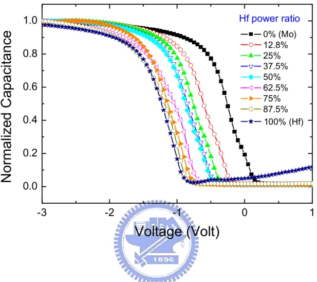
(47) the EOT as well as the metal work function value [14].. 2.3 RESULTS AND DISCUSSION The as-deposited high frequency (1MHz) C-V characteristics of capacitors gated by Hf-Mo binary alloys, pure Mo, and pure Hf films are shown in Fig. 2.1. The negative flat-band voltage shift with the increase of Hf power ratio can be observed. To eliminate the contribution of oxide fixed charges, C-V measurements of MOSCAP devices with several oxide thicknesses were performed to generate the VFB versus EOT plot as shown in Fig. 2.2. All samples exhibit linear relationships from which work function values of binary alloys can be extracted as listed in Table 2.1.. Figure 2.3 exhibits the (110) morphology for the pure Mo film. The extracted work function value (4.93eV) of the (110) oriented Mo is closely consistent with previous reports [13]. However, the as-deposited Mo with (110) orientation is different from the previous report [15], and this would be attributed to the different deposition conditions. Figure 2.4 exhibits the small the hysteresis for the 50% Hf power ratio co-sputtering sample, which is believed to suffer from the most series sputtering damage. Accordingly, the good process quality can be demonstrated.. The C-V curves of as-deposited and post-400 ℃ sintering pure Hf gated capacitor are shown in Fig. 2.5. Obvious EOT variation along with the VFB shift after annealing illustrates the poor thermal stability of Hf on SiO2 and exclude Hf from gate candidates even in the gate last process [16]. By contrast, HfxMo(1-x) gated capacitors exhibit better thermal stability on SiO2 as shown in Fig. 2.6. The dependence of Φm 26.
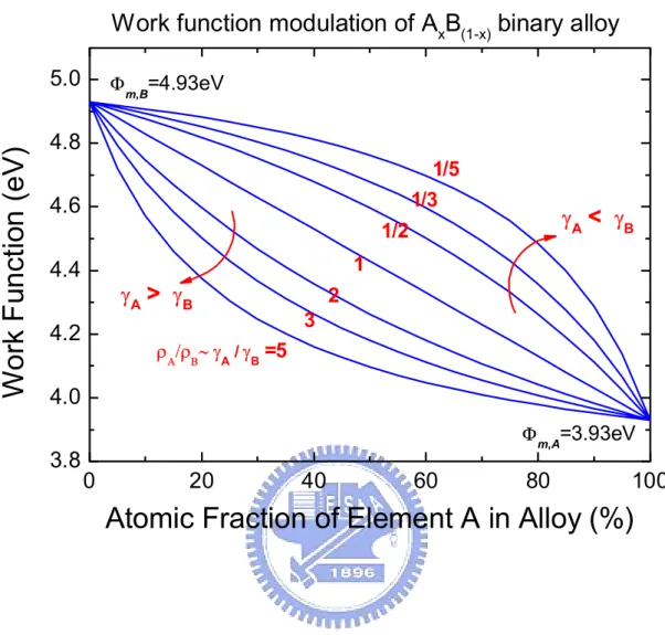
(48) and EOT variation on annealing conditions for HfxMo(1-x) also indicates that the thermal stability of all alloy samples can be at least higher than 400℃ as shown in Fig. 2.7.. In Fig. 2.7, the decreases of EOT at certain temperature for alloy samples, except for the one with 25% Hf power ratio, are similar to that for the pure Hf sample. The noticeable EOT decrease and the corresponding work function variation might be attributed to that partial SiO2 gate dielectric was transformed into high-k materials, such as HfO2 or HfSixOy, due to the Hf-SiO2 interaction. For the 25% alloy sample, the abnormal EOT increase along with relative small work function variation can be observed. We speculate that the lower Hf concentration might make the effect of Hf-SiO2 interaction be masked by the extra Si-substrate oxidation due to the oxygen contamination. In the case of sample gated by pure Mo, the small amount of Φm increase (18meV) and the negligible EOT variation (0.08nm) after 950℃ RTA demonstrate the superior thermal stability of Mo on SiO2 gate dielectric. Although the thermal stability seems to be degraded with the increasing of the Hf atomic fraction in the Hf-Mo binary alloy, HfxMo(1-x) still can be adopted as gate material in a gate-last SiO2 CMOS process. It is worth to note that, alloy samples with Hf power ratio lower than 50% can possess work function value suitable for advanced devices and exhibit thermal stability up to 700℃. In comparison with other reported candidates, the thermal stability of Hf-Mo alloy is lower than that for Ru-Ta alloy [9], but higher than that for Pt-Ta alloy [11].. In 1974, Gelatt and Ehrenreich proposed that the work function of an AxB(1-x) alloy can be approximately expressed as [17] :. 27.
(49) Φ m ( x ) = xΦ m , A + (1 − x )Φ m ,B. (Φ + x (1 − x ). − Φ m ,B )(ρ A ρ B − 1) x ⋅ ρ A ρ B + (1 − x ). m,A. (1.1). In this equation, Φm,A and Φm,B are work function values of pure element A and B, respectively. ρA and ρB are effective density of states in Fermi level for pure element A and B, respectively. In this equation, the first two terms represent that the work function of the binary alloy is a linear combination of that of each pure element. On the other hand, the last term will lead to a deviation from the linear relationship. According to the theory of heat capacity of metal, the observable Sommerfeld factor γ of a metal is directly proportional to its density of state in Fermi level ρ [18].. The calculated results of eq. (1) are shown in fig. 2.8 where several γ ratios are used and values of Φm,A and Φm,B are set to be 3.93 and 4.93, respectively, for convenience. As expected, the work function modulation will deviate from the linear behavior with the difference in γ values between two metals. For a non-linear behavior, work function modulation can be roughly divided into the flat and sharp regime. In the flatter regime, the alloy system would be less susceptible to the composition and process variation, but the Φm modulation efficiency will be lower. On the other hand, the alloy system will be more sensitive to the process variation but possess higher Φm modulation efficiency in the sharper regime. By contrast, the linear work function modulation can provide a compromise between the modulation efficiency and immunity to the process variation throughout the whole modulation range.. According to the binary alloy phase diagram of Hf-Mo system [19] shown in fig. 2.9, an abrupt work function modulation can be excluded since no specific compound will be formed under 1000℃. Moreover, the Sommerfeld factors for Hf and Mo are 28.
(50) 2.16 and 2.0, respectively [18]. Therefore, a continuous and almost linear work function modulation using the HfxMo(1-x) solid solution can be expected. The calculated and experimental results of work functions of HfxMo(1-x) alloys are shown in fig. 2.10. Compared with the experimental data, a good consistency with only a mildly shift in the lower Hf power ratio regime can be observed. This deviation may be attributed to the difference between the Hf power ratio and the Hf atomic fraction due to a relatively lower deposition rate of Mo in this work.. The XRD spectra and AES depth profile of the co-sputtering sample are shown in fig. 2.11 and fig. 2.12, respectively. An amorphous film with uniform composition and abrupt interface is observed. It is worth to note that the relatively lower composition of Mo compared to that of Hf in the co-sputtering sample as shown in fig. 2.12 also demonstrates our speculation about the deviation observed in Fig. 2.10.. 2.4 SUMMARY The continuous and almost linear work function adjustment using HfxMo(1-x) is demonstrated for the first time. The work function value of Hf-Mo binary alloy deposited by co-sputtering ranges from 3.93eV (Φm of pure Hf) to 4.93eV (Φm of pure Mo) and depends on the sputtering power ratio of each target. The thermal stabilities of Hf-Mo binary alloys on SiO2 degrade with the increase of Hf atomic fraction, but all Hf-Mo binary alloys still possess thermal stabilities at least higher than 400℃. The Hf-Mo binary alloys can be used in a gate-last SiO2 CMOS process.. 29.
(51) REFERENCES. [1]. E. M. Vogel, K. Z. Ahmed, B. Hornung, W. K. Hensen, P. K. McLarty, G. Lucovsky, J. R. Hauser, and J. Wortman, “Modeled tunnel currents for high dielectric constant dielectrics,” IEEE Trans. on Electron Devices, vol.45, pp.1350-1355, June 1998.. [2]. Q. Lu, D. Park, A. Kalnitsky, C. Chang, C. –C. Cheng, S. P. Tay, T. –J. King, and C. Hu, “Leakage current comparison between ultra-thin Ta2O5 films and conventional gate dielectrics,” IEEE Electron Device Letters, vol.19, pp.341-342, Sept. 1998.. [3]. K. F. Schuegraf, C. C. King, and C. Hu, “Impact of polysilicon depletion in thin oxide MOS technology,” in Proc. Tech. Papers 1993 Int. Symp. VLSI Technology, Systems, and Applications, 1993, pp.86-90.. [4]. James R. Pfiester, Frank K. Baker, Thomas C. Mele, H. H. Tseng, Philip J. Tobin, James D. Hayden, James W. Miller, Craig D. Gunderson, and Louis C. Parrillo, “The effects of boron penetration on p+ polisilicon gated PMOS devices,” IEEE Trans. on Electron Devices, vol.37, no.8,. pp.1842-1851,. August 1990. [5]. H. F. Luan, B. Z. Wu, L. G. Kang, R. Vrtis, D. Roberts, and D. L. Kwong, “Ultra thin high quality Ta2O5 gate dielectric prepared by in-situ rapid thermal processing,” in IEDM Tech. Dig., 1998, pp.609-612.. [6]. C. H. Lee, H. F. Luan, W. P. Bai, S. J. Lee, T. S. Jeon, Y. Senzaki, D. Roberts, and D. L. Kwong, “MOS characteristics of ultra thin rapid thermal CVD ZrO2 and Zr silicate gate dielectrics,” in IEDM Tech. Dig., 2000, pp.27-30.. [7]. Leland Chang, Stephen Tang, T. J. King, Jeffrey Bokor, and C. Hu, “Gate 30.
(52) length scaling and threshold voltage control of double-gate MOSFETs,” in IEDM Tech. Dig., 2000, pp.719-722. [8]. Qiang Lu, Y. C. Yeo, Pushkar Ranade, Hideki Takeuchi, T. J. King, and C. Hu, “Dual-metal gate technology for deep-submicron CMOS transistors,” in Symp. on VLSI Tech., 2000, pp.72-73.. [9]. Huicai Zhong, Shin-Nam Hong, You-Seok Suh, Heather Lazar, Greg Heuss, and Veena Misra, “Properties of Ru-Ta alloys as gate electrodes for NMOS and PMOS silicon devices,” in IEDM Tech. Dig., 2001, pp.467-480.. [10]. JaeHoon Lee, Huicai Zhong, You-Seok Suh, Greg Heuss, Jason Gurganus, Bei Chen, and Veena Misra, “Tunable work function dual metal gate technology for bulk and non-bulk CMOS,” in IEDM Tech. Dig., 2002, pp.359-362.. [11]. Bing-Yue Tsui and Chih-Feng Huang, “Wide range work function modulation of binary alloys for MOSFET application,” IEEE Electron Device Letters, vol.24, pp.153-155, March 2003.. [12]. S. H. Bae, W. P. Bai, H. C. Wen, S. Mathew, L. K. Bera, N. Balasubramanian, N. Yamada, M. F. Li, and D. L. Kwong, “Laminated metal gate electrode with tunable work function for advanced CMOS,” in Symp. on VLSI Tech., 2004, pp.188-189.. [13]. Pushkar Ranade, Yang-Kyu Choi, Daewon Ha, Aditya Agarwal, Michael Ameen, and Tsu-Jae King, “Tunable work function molybdenum gate technology for FDSOI-CMOS,” in IEDM Tech. Dig., 2002, pp.363-366.. [14]. K. J. Yang, Y. -C. King, and C. Hu, “Quantum effect in oxide thickness determination from capacitance measurement,” in Symp. on VLSI Tech., 1999, pp.77-78.. 31.
(53) [15]. P. Ranade, Y. C. Yeo, Q. Lu, H. Takeuchi, T-J. King, and C. Hu, “Molybdenum metal gate MOS technology for post-SiO2 gate dielectrics,” in Mat. Res. Soc. Symp., vol.611, 2000, pp.C3.2.1-C3.2.6.. [16]. A. Yagishita, T. Saito, K. Nakajima, S. Inumiya, Y. Akasaka, Y. Ozawa, G. Minamihaba, H. Yano, K. Hieda, K. Suguro, T. Arikado, and K. Okumura, “High performance metal gate MOSFETs fabricated by CMP for 0.1µm regime,” in IEDM Tech. Dig., 1998, pp.785-788.. [17]. C. D. Gelatt Jr., and H. Ehrenreich, “Charge transfer in alloys: AgAu,” Phys. Rev. B, vol. 10, no. 2, pp.398-415, July 1974.. [18]. C. Kittel, Introduction to Solid State Physics, 7th ed. New York: Wiley, 1996, pp.151-157.. [19]. Massalski Thaddeus B. ed., Binary Alloy Phase Diagrams, Metal Park, Ohio: American Society for Metals, 1990, pp.2088-2089.. 32.
(54) Sample. Hf power (W). Mo power (W). Hf power ratio (%). Φm (eV). ctrl.. 0. 150. 0 (pure Mo). 4.932. 1-1. 22. 150. 12.8. 4.727. 1-2. 50. 150. 25. 4.597. 1-3. 90. 150. 37.5. 4.492. 1-4. 150. 150. 50. 4.350. 1-5. 150. 90. 62.5. 4.213. 1-6. 150. 50. 75. 4.150. 1-7. 150. 22. 87.5. 4.062. ctrl.. 150. 0. 100 (pure Hf). 3.930. Table 2.1. Sample conditions and extracted Φm of co-sputtering experiment. (alloy samples : 400℃, 30s;control samples : as-deposited). 33.
(55) Hf power ratio. Normalized Capacitance. 1.0. 0% (Mo) 12.8% 25% 37.5% 50% 62.5% 75% 87.5% 100% (Hf). 0.8 0.6 0.4 0.2 0.0. -3. -2. -1. 0. Voltage (Volt). Fig. 2.1. C-V curves of as-deposited co-sputtering samples. Wide-ranging flat band voltage shift can be observed.. 34. 1.
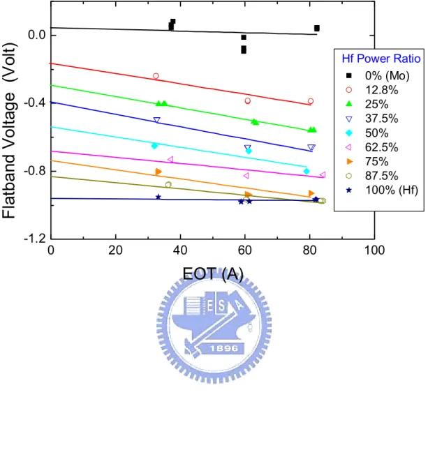
(56) Flatband Voltage (Volt). 0.0 Hf Power Ratio 0% (Mo) 12.8% 25% 37.5% 50% 62.5% 75% 87.5% 100% (Hf). -0.4. -0.8. -1.2. 0. 20. 40. 60. 80. 100. EOT (A). Fig. 2.2. All samples (Table I.) exhibited linear behavior in VFB vs. EOT curves from which work function of each alloy could be extracted. (alloy samples : 400℃, 30s; control samples : as-deposited). 35.
(57) Mo (110). Intensity (Arb. Unit). Si-sub.. pure Mo film. 20. 30. 40. 50. 2θ (Degree). Fig. 2.3. The as-deposited pure Mo film is found to have (110) orientation.. 36. 60.
(58) -10. 5.0x10. inv to acc acc to inv. -10. Capacitance (F). 4.0x10. -10. 3.0x10. -10. 2.0x10. -10. 1.0x10. Co-sputtering sample 50% Hf power ratio EOT = 31A. 0.0 -3. -2. -1. 0. 1. Voltage (Volt). Fig. 2.4. Process quality was demonstrated, since the 50% Hf power ratio sample suffering maximum power summation during metal deposition still exhibited negligible hysteresis.. 37.
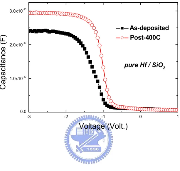
(59) -10. Capacitance (F). 3.0x10. As-deposited Post-400C -10. 2.0x10. pure Hf / SiO2 -10. 1.0x10. 0.0 -3. -2. -1. 0. 1. Voltage (Volt.). Fig. 2.5. C-V curve of post-400℃ annealing Hf gated capacitor shows noticeable EOT variation and flatband voltage shift.. 38.
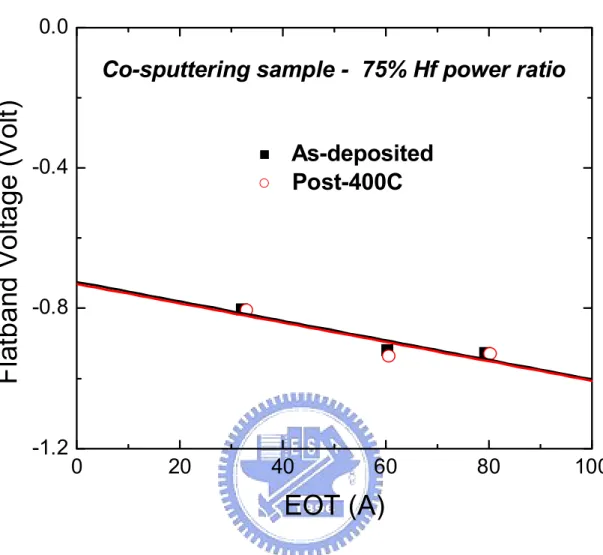
(60) 0.0. Flatband Voltage (Volt). Co-sputtering sample - 75% Hf power ratio. As-deposited Post-400C. -0.4. -0.8. -1.2. 0. 20. 40. 60. 80. 100. EOT (A). Fig. 2.6. Post-400℃ annealing co-sputtering sample shows negligible work function variation.. 39.
(61) Delta Φm (eV). 0.3 0.2 0.1 0.0 -0.1. 100% (Hf) 25%. Delta EOT (A). 10. 75% 0% (Mo). 50%. 5 0 -5 -10 -15. as-deposit. 400C. 500C. 600C. 700C. 800C. 900C. 950C. Annealing Condition. Fig. 2.7. The dependence of Φm and EOT variation on annealing temperature show that the thermal stability of alloy samples can be at least higher than 400℃.. 40.
(62) Work function modulation of AxB(1-x) binary alloy. Work Function (eV). 5.0. Φm,B=4.93eV. 4.8 1/5 1/3. 4.6. γA < γB. 1/2 1. 4.4. γA > γB. 4.2. 2 3. ρΑ/ρΒ ∼ γA / γB =5. 4.0 3.8. Φm,A=3.93eV. 0. 20. 40. 60. 80. 100. Atomic Fraction of Element A in Alloy (%). Fig. 2.8. Calculated work function value versus atomic fraction in binary alloy as a function of γ ratio. Metals with similar γ (Sommerfeld factor) will lead to a linear work function modulation which is a compromise between modulation efficiency and immunity to process variation. (Φm.A and Φm.B are set to be 3.93 and 4.93eV for convenience). 41.
(63) Fig. 2.9. The phase diagram of Mo-Hf system.. 42.
(64) Hf Atomic Fraction (%) 0. 40. 60. 80. Ev. 5.2. Work Function (eV). 20. 100 5.17. 5.0. 4.95. 4.8. Experimental Theory (γ Hf / γΜο = 1.08). 4.6. 4.52. 4.4 4.2. Ec. 4.05. 4.0 3.8. 0. 20. 40. 60. 80. 100. Hf Power Ratio (%). Fig. 2.10. Comparison between experimental (Table I.) and theoretical work function values. A slightly deviation in lower Hf power ratio regime may be attributed to different sputtering rate between Hf and Mo. (γHf = 2.16, γMo = 2.0 are used for calculation). 43.
(65) 50% alloy sample deposited by co-sputtering. Intensity (Arb. Unit). 900C 800C 700C 600C 500C as-deposited. 30. 40. 50. 60. 2θ (Degree). Fig. 2.11. XRD spectra of 50% Hf power ratio co-sputtering sample exhibited an amorphous film structure and only the c-Si was featuring.. 44.
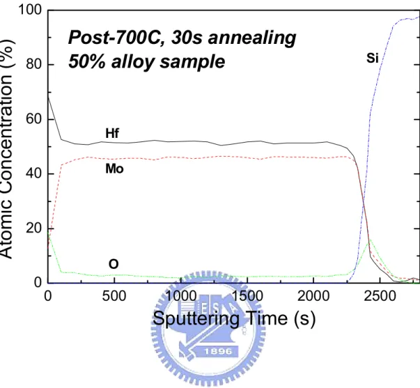
(66) Atomic Concentration (%). 100. Post-700C, 30s annealing 50% alloy sample. 80. 60. Si. Hf Mo. 40. 20 O. 0. 0. 500. 1000. 1500. 2000. 2500. Sputtering Time (s). Fig. 2.12. AES profile of post-annealing 50% Hf power ratio co-sputtering sample. A uniform composition and abrupt interface can be observed.. 45.
(67) Chapter 3. Integratable Dual Metal Gate Technology Using HfxMo(1-x) Binary Alloys. 3.1 BACKGROUNDS AND MOTIVATION In the previous chapter, the almost linear and continuous work function modulation behavior of Hf-Mo binary alloys is demonstrated. In the view of process integration, a suitable integration technique should be introduced to avoid the process induced gate dielectric integrity degradation.. Here we propose a dual metal gate technology which employs Mo and HfxMo(1-x) as gate electrodes for p- and n-channel devices, respectively. In this case, the HfxMo(1-x) electrode in the proposed dual metal gate technology is formed by metal intermixing. Metals need not to be removed from the dielectric interface so that the uniformity and integrity of gate dielectric can be preserved. Furthermore, a parameter called the optimal annealing temperature, TA,opt, is expected to provide a prospective work function modulation without causing the EOT variation. The value of TA,opt will strongly affect the application of the proposed technique.. Moreover, since the phenomenon of metal intermixing is based on solid diffusion, we demonstrate that the optimal annealing temperature, TA,opt, can be raised by increasing the total metal thickness (TM = THf + TMo). Consequently, it is likely to 46.
(68) overcome the thermal stability issue in conventional CMOS process by using an appropriate metal thickness. In addition, the composition and work function of HfxMo(1-x) are demonstrated to depend on the thickness combination of metal layers. At the top surface of the gate electrode, the oxidation of Hf which will lead to an extra Hf consumption was observed. A modified multilayer structure (TiN/Mo/Hf/Mo) was fabricated and verified to improve the immunity to metal oxidation. In addition, a quadratic equation relating the work function (Φm) to composite metal thickness ratio (TR = THf / TMo) is also derived. Good consistency with the experimental data assures the possibility of precise metal work function adjustment.. 3.2 EXPERIMENT Figure 3.1 shows a practicable fabrication process for the proposed dual metal gate technology that uses Mo and HfxMo(1-x) as gate electrodes. After LOCOS isolation and the gate dielectric deposition, the first layer metal Mo and the second layer metal Hf are deposited over the entire wafer. A non-critical lithography step is performed and the second layer metal Hf is then selectively removed from the PMOS side. After gate electrodes patterning and S/D implantation, the thermal annealing is performed for dopant activation and metal intermixing at the NMOS side simultaneously.. To demonstrate this technique, MOSCAP devices were fabricated. The process flow is similar to that of co-sputtering experiment, except that Mo and Hf are deposited in sequence. The Mo gate has been reported to possess high thermal stability (> 1000℃) on SiO2 gate dielectric [1]. Moreover, the work function value of 47.
數據
+7

相關文件
With the proposed model equations, accurate results can be obtained on a mapped grid using a standard method, such as the high-resolution wave- propagation algorithm for a
Promote project learning, mathematical modeling, and problem-based learning to strengthen the ability to integrate and apply knowledge and skills, and make. calculated
Lin, A smoothing Newton method based on the generalized Fischer-Burmeister function for MCPs, Nonlinear Analysis: Theory, Methods and Applications, 72(2010), 3739-3758..
• Gauss on Germain: “But when a person of the sex which, according to our customs and prejudices, must encounter infinitely more difficulties than men to.. familiarize herself with
A marble texture can be made by using a Perlin function as an offset using a Perlin function as an offset to a cosine function. texture = cosine( x +
State value function: when using
Since Dolby AC-3(abbreviated as AC-3) is the main technology of the surrounding sound format, in this thesis, we proposes a data model for mining the relationship between
Several methods that modulation effective work function to maintain p-type gate material is the direction of future research, sush as microwave annealing with plasma
