砷化鎵低噪音假晶高電子遷移率電晶體之銅金屬化導線製程
120
0
0
全文
(2) 砷化鎵低噪音假晶高電子遷移率電晶體之 銅金屬化導線製程 Copper-Metallized Interconnects on GaAs Low Noise Pseudomorphic High Electron Mobility Transistors. 研 究 生:張晃崇. Student: Huang-Choung Chang. 指導教授:張. Advisor: Dr. Edward Yi Chang. 翼 博士. 國立交通大學 材料科學與工程研究所 博士論文 A Dissertation Submitted to Department of Materials Science and Engineering College of Engineering National Chiao Tung University In Partial Fulfill of the Requirements For the Degree of Doctor of Philosophy in Engineering 2004 Hsinchu, Taiwan, Republic of China. 中華民國九十三年六月二十一日 2.
(3) Contents. Acknowledgement (in Chinese)……………...…………………………5. Abstract (in Chinese)……………………………………………………6 Abstract (in English)……………………………………………………8 Chapter 1 Introduction………………………………………………10 Chapter 2 Study of Ti/W/Cu, Ti/Co/Cu and Ti/Mo/Cu multilayer structures as Schottky metals for GaAs diodes…………………...26 2.1 Phase Diagrams..………………………………………………………………26 2.2 Sample Preparation.………….………………………………………………..26 2.3 X-ray Diffraction Patterns (XRD)..……………………………………………27 2.4 Measurement and Charactersization…………………………………………..28. Chapter 3 Fabrication of Low Noise GaAs PHEMT………………...44 3.1 Pseudomorphic High Electron Mobility Transistor (PHEMT) Device Structure ……………………...………………………………………………..44 3.2 Device Process Flow…………………………………………………………...44 3.3 Device Isolation………………………………………………………………...45 3.4 Ohmic Contact………………………………………………………………….46 3.5 Gate Formation…………………………………………………………………48 3.6 Device Passivation……………………………………………………………..49. 3.
(4) Chapter 4 Technology Development of the Cu-Metallized Airbridges ...…………………………………………………………....59 4.1 Device Passivation……………………………………………………………..59 4.2 Comparison between Au Airbridge and Cu Airbridge Processes………60 4.3 Thin Metal Structure Used for Cu Airbridges on PHEMTs fabricated with Au Metallized Contacts………………………………………………………61 4.4 Cu Electroplating………………………………………………………….66. Chapter 5 Airbridge Interconnects Process………………………….90 5.1 Airbridge Process Flow……………………………………………..………….90 5.2 Sample Preparation……………………………………………………………90 5.3 The First Photolithography for Plating Vias……………………………………91 5.4 Thin Metal Deposition………………………………………………………….93 5.5 The Second Photolithography for Plating Areas…………………………….....93 5.6 Electroplating…………………………………………………………………..95 5.7 Plating PR. Removal and Thin Metal Etching…………………………………96. Chapter 6 Electrical Characteristics and Thermal Stability of PHEMTs Fabricated with Cu-Metallized Airbridges………....108 6.1 DC Characteristics…………………………………………………………….106 6.2 Noise and Gain Performance.……………………………………………..107 6.3 The Unity-Current-Gain Frequency…………………………………………..107. Chapter 7 Conclusions………………………..……………………...119. 4.
(5) 致謝 首先我要感謝我的博士班與碩士班指導教授張翼博士,他誠摯地邀請我加入 這個實驗室,提供一個歷練的機會、最好的資源以及耐心的指導,使我能夠參與 一個砷化鎵高頻通訊元件實驗線的建立。這個經驗不但非常有趣,而且很難得! 我的碩士班共同指導教授陳三元博士就像是我的好朋友,他非常尊重我對研 究生涯做的每個決定。在他無私無怨的指導之下,我可以有最大的空間去發展我 有興趣的題目。在我的學業面臨重要抉擇時,他也非常熱心地給我一些中肯的建 議。 我要感謝王聖評學長與賴永齡博士多年來在製程整合上提供寶貴經驗。另 外,李承士博士、李澤倫先生、羅廣禮博士等前輩在我博士班研究生期間給我許 多的指導及協助。 陳仕鴻博士是我在交大研究生期間的最佳拍檔,我們的合作已經將近六年, 能夠碰到這麼溫文儒雅又有默契的搭檔真是人生一大快事! 在我的論文研究上,我要特別感謝實驗室同學張尚文同學、連亦中同學、褚 立新同學、黃瑞乾同學、吳偉誠同學、陳克弦同學和董福慶同學給我的協助。而 在實驗室的事務上,我還要謝謝梁坊旭先生、詹前璋先生、林岳欽同學、楊宗熺 同學、謝炎璋同學、李晃銘同學和徐金鈺同學。除此之外,歷年來還有許許多多 的實驗室同學默默的幫助我。這些實驗室的同仁及同學是我在研究上支持我的最 大後盾。 在學校的奈米中心的眾多同仁中,我要特別感謝陳悅婷小姐和何惟梅小姐。 沒有他們的包容與協助,實驗室的眾多研究計劃不可能順利達成。 最後,我要感謝我家人,你們辛苦了!. 5.
(6) 砷化鎵低噪音假晶高電子遷移率電晶體之 銅金屬化導線製程. 研究生:張晃崇. 指導教授:張 翼 博士. 國立交通大學材料科學與工程研究所. 摘要. 這篇論文研究使用在砷化鎵上面的銅金屬擴散障礙層之特性,並探討銅金屬 化蕭特基接觸以及銅金屬化導線製程應用在砷化鎵元件上之可行性。在這些擴散 障礙層的研究中,耐火金屬以及耐火金屬之氮化物被應用在銅金屬化蕭特基二極 體以及銅金屬化導線製程之製作。 本篇研發之砷化鎵蕭特基二極體,其蕭特基結構使用銅金屬,並使用耐火金 屬作為障礙層。這種蕭特基結構具有比傳統鈦/鉑/金蕭特基結構更低的串聯電 阻。根據電性及材料分析,鈦/鈷/銅以及鈦/鉬/銅之熱穩定性可達攝氏四百度, 而鈦/鈷/銅蕭特基結構之熱穩定性可達攝氏三百度。總而言之,銅金屬化蕭特基 結構具有優良的電性及熱穩定性,並且可應用於砷化鎵元件的蕭特基金屬製程。 在本實驗中使用氮化鎢作為銅金屬化導線製程之擴散障礙層。這是由於氮化 鎢和傳統製程上有高度的相容性。本實驗發展使用銅金屬化導線之砷化鎵低噪音 假晶高電子遷移率電晶體之製程。此製程使用濺鍍氮化鎢作為擴散障礙層並使用 鈦金屬作為附著層。製作出來的低噪音砷化鎵假晶高電子遷移率電晶體在操作頻 率為十八兆赫茲時,元件噪音最低可達一點零九分貝、相關增益值可達六點九分 貝。經過攝氏兩百五十度的高溫退火二十個小時以後,銅金屬以及下層的接觸金 屬間並沒有金屬原子交互擴散的現象;元件特性在經過熱退火以後並未產生明顯 6.
(7) 的變化。這個結果顯示銅金屬化空氣橋製程可以應用在低噪音假晶高電子遷移率 電晶體上。. 7.
(8) Copper-Metallized Interconnects on GaAs Low Noise Pseudomorphic High Electron Mobility Transistors. Student: Huang-Choung Chang. Advisor: Dr. Edward Yi Chang. Department of Materials Science and Engineering National Chiao Tung University. Abstract. In this dissertation, the feasibilities of Cu-metallized Schottky contacts on GaAs and Cu-metallized interconnects for GaAs devices were studied. Diffusion barrier materials for Cu metallization on GaAs were investigated. Several refractory metals and metal nitrides were used as the diffusion barrier and applied to the Schottky contact and interconnect airbridge applications. Schottky structures with Cu and refractory metals as the diffusion barrier for GaAs Schottky diodes were evaluated. These structures have lower series resistances than the conventionally used Ti/Pt/Au structure. Based on the electrical and material characteristics, the Ti/W/Cu and Ti/Mo/Cu Schottky structures are thermally stable up to 400 °C; the Ti/Co/Cu Schottky structure is thermally stable up to 300 °C. Overall, the Cu-metallized Schottky structures have excellent electrical characteristics and thermal stability, and can be used as the Schottky metals for GaAs devices. For airbridge fabrication, tungsten nitride was chosen as the diffusion barrier for Cu-airbridged PHEMT due to its compatibility with the airbridge process. A GaAs pseudomorphic high electron mobility transistor (PHEMT) with Cu-metallized airbridges was successfully developed. Sputtered WNx was used as the diffusion barrier and Ti was used as the adhesion layer to avoid the peeling problem between 8.
(9) Au/WNx and WNx/Cu. When tested at 18 GHz, the fabricated low noise GaAs PHEMT with Cu interconnect had the lowest noise figure of 1.09 dB and the associated gain was 6.9 dB. After thermal annealing at 2500C for 20 hours there’s no interatomic diffusion between Cu and underlying contact metals and the devices showed little change in the device performance. These results show that the Cu-metallized airbridges can be used as the interconnects for low noise PHEMTs.. 9.
(10) Chapter 1 Introduction. The Cu metallization process has become popular in Si device manufacturing and has been widely studied, but there are very few reports about Cu metallization process for GaAs-based devices [1-3]. In this work, Cu-metallized Schottky contacts and Cu-metallized interconnects for GaAs devices were studied. Various materials have been considered for metallization of integrated circuits (IC). Au and Cu possess several remarkable features: both have low resistivity (2.2 µΩ-cm for Au; 1.67 µΩ-cm for Cu), and provide high resistance against electromigration related failures [4]. Au has not been used in metallization for Si-based devices. However, Au is extensively used for GaAs device fabrication, mainly due to its high electrical conductivity and relative chemical inertness [5]. Au metallization needs the use of adhesion layers, like Ti or Cr; and also needs the use of barrier layers such as platinum or palladium to impede its diffusion into GaAs [6]. Cu metallization is widely used as the interconnect material in the Si IC technology. This is principally because of its low resistivity (1.67 µΩ-cm), which results in a lower RC time delay, and the enhancements in the resistance of electromigration and stress-induced failures [7,8], which greatly improves the device performance and reliability. The Cu metallization process has become progressively popular in the Si IC industry ever since IBM scientists announced a remarkable advance in Cu metallization for semiconductor process in September 1997 [9–11]. Recently Cu has been widely employed by major semiconductor companies as interconnect material of the ultralarge-scale integration (ULSI) circuits, the process involves damascene patterning techniques with compatible low dielectric constant 10.
(11) materials [12-23]. The Ti/Pt/Au Schottky contact is the most widely used structure for the fabrication. of. metal-semiconductor. field-effect. transistors. (MESFETs),. high-electron-mobility transistors (HEMTs), and Schottky diodes. In this study, the top Au layer of the Schottky structure was replaced by Cu. This has the advantages of reduced electrical resistivity and production cost when compared with the use of Au. The Pt layer was replaced by the transition metals, such as W, Co and Mo, due to the better anti-diffusion capability and the electrical conductivity of these transition metals. According to the binary alloy phase diagrams [24], there is no formation of intermetallic compounds between W (Co, Mo) and Cu. Thus, the thermal stability of these Cu-metallized Schottky structure including Ti/W/Cu, Ti/Co/Cu and Ti/Mo/Cu was investigated in this study. The detailed study of Cu-metallized Schottky contacts will be described in Chapter 2. Conventionally, plated Au was employed for airbridge interconnects on GaAs devices, including MESFETs and HEMTs. Plated Au has high electrical conductivity, is resistant to oxidation and ductile. However, Au is expensive, which causes the high cost for the GaAs device fabrication. At present, Cu is one of the most attractive materials for interconnect metallization of ULSI circuits because of its low resistivity and excellent resistance against electromigration. However, key issues need to be solved if Cu interconnections are used for GaAs device metallization: 1) It is necessary to use a thin barrier layer with good linear conformality with Cu to block Cu diffusion especially for narrow, high aspect-ratio structures. 2) A passivation layer is required to prevent the oxidation of Cu surface [25]. In this work, Cu replaces Au as the interconnect material used for the airbridges in the GaAs PHEMTs and WNx was used as the diffusion barrier. The goal of the research is to find a reliable diffusion barrier for Cu metallization of GaAs devices in 11.
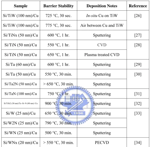
(12) order to reduce the production cost of the GaAs devices and to provide comparable or even better thermal and electrical conductivities for the interconnects. The major challenges for the integration of Cu metallization are the choice of suitable diffusion barrier material and the deposition techniques of the diffusion barrier and the Cu layer. The barrier layer should be as thin as possible so that it would not affect the interconnect resistance while still acting as a good barrier against Cu diffusion. The choice of multilayer thin films needs to consider the following aspects: the electrical resistivity, mechanical stress, chemical inertness, thermal stability, adhesion characteristics, film deposition techniques, and easiness of film patterning [6]. Refractory metal is a good choice as the diffusion barrier materials. This is because of its high melting point. Its solubility in Cu was very low even though at high temperatures. However, the sheet resistance of Cu increases rapidly at 400 ℃ annealing when using a single refractory metal as the diffusion barrier, like Cu/Ta/Si, Cu/Ti/Si, and Cu/W/Si. It implies the Cu atoms diffuse into Si and forms copper silicide. The single metal diffusion barrier layer is a polycrystalline structure with grain boundaries. The grain boundaries provide fast diffusion paths for the Cu because of the high diffusion coefficient along the grain boundaries. Cu diffuses through the grain boundaries of the diffusion barrier layer easily into the Si junction region even at low annealing temperatures and causes the device failure. Refractory metal nitrides such as TiN, TaN and WNx have been investigated due to their better thermal stabilities, good adhesion, and low resistivities. Therefore, these transition metal nitrides, which have high melting points, relatively high thermal stability, chemical inertness, and low electrical resistivity, would not form metallic compounds with Cu. Some of the results of the investigations of the refractory metals and refractory metal nitrides as the diffusion barriers for Si are listed in Table 1 [26-34]. 12.
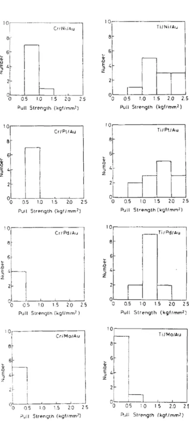
(13) The thermal stabilities of these barrier layers with Cu are summarized in Table 1. These barrier layers include TiW, TiN, Ta, TaN, Ta-Si-N and WNx. Most barrier materials are stable with Cu up to 550 °C. The temperature is high enough for current metallization processes. Only a few investigations of the Cu metallization process on GaAs devices have been reported [1-3, 35-41], and Ta and TaN were employed as the diffusion barriers in these papers [1–3]. In this work, we use WNx as the diffusion barrier between Cu and Au, and successfully apply WNx to the Cu metallization of the airbridge interconnects of the AlGaAs/InGaAs low noise pseudomorphic high electron mobility transistors (LN-PHEMTs). 2.5 µm Cu was electroplated on the sputtered Cu seed layer and the WNx barrier layer to form the airbridges on the Au contacted PHEMTs. The fabricated low noise PHEMTs with Cu airbridges were thermally annealed in order to evaluate the thermal stability of WNx as the barrier between Cu and underlying Au-based contacts [41]. However, the peelings off problem of the Cu airbridges were observed in certain areas of the devices. The peeling interface was observed between Au/WNx and WNx/Cu interfaces. This implies that the adhesion between these films was not good. From conventional Au metallization, adhesion of the Au film on the oxide substrate can be improved through the deposition of an intermediate metal film (Ti, Cr, W) [42]. The most common species of adhesion film for ball-limited-metal (BLM) system under solder bumps are Ti and Cr. Ken’ichi Mizuishi et al. have investigated the mechanical pull-strength of the BLM layers formed under controlled-collapse solder (lead-5 wt % tin) bumps for flip-chip interconnections [43]. All BLM systems used here consist of a triple-layer deposited with Cr or Ti as an adhesive, Ni, Pt, Pd, or MO as a barrier, and Au as the surface metal. Using test chips with these BLM 13.
(14) systems, mechanical pull-strength values of solder-bump joints were obtained as shown in Figure 1.1. From a simple comparison between the mechanical strength values, they found that the BLM systems with Ti adhesive metal showed generally superior solder-joint strength than those with Cr, independent of the barrier metal used. This is due to the presence of the joint fracture mode which is closely related to the kind of adhesive metal used. It is also found that, with the same adhesive metal, greater solder-joint strength appears in the order of Ni, Pt, Pd, and Mo. Therefore, we decided to use Ti as the adhesion layer for our multilayer metallization system to overcome the peeling off problem of the airbridges. As a result, new multilayer schemes, Ti/WNx/Ti/Cu, were used in this study to improve the film adhesion on Au pad and on silicon nitride passivation layer. The Ti thin films were inserted between Au/WNx layers and between Cu/WNx layers respectively. The most upper two layers, Ti/Cu, which were used extensively in solder bump fabrication as an adhesion and seed-conducting layer between electroplated Cu and WNx layers [44,45]. There are reasons for it. The adhesion is good between Ti and Au layers because Ti diffuses into Au fast, producing Au-rich intermetallic compounds [46]. The Ti/Au/Ti scheme is the traditional airbridges process for GaAs devices. For the Ti/WNx interface, F. C. T. SO et al. suggested that nitrogen in the W-N layer redistributed into Ti layer after annealing at 550 °C for the Si/Ti/WNx/Al samples [47]. They attributed this redistribution of nitrogen to the stronger affinity of Ti with nitrogen than with W. It implied that the Ti layer reduces WNx to W upon annealing at 550 °C and forms a good Ti-N interface with good adhesion. For the SiNx/Ti boundary, T. W. Orent et al. suggested that Ti reduces the Si from the silicon nitride during deposition process and forms TiN and free Si. The free Si reacts with additional Ti at the Ti/TiN interface to form a silicide in the SiNx/Ti/Cu samples at 14.
(15) above 500 °C annealing and thus improve the adhesion of this material system [48]. Kazuhide Abe et al. introduced a Cu/Ti/TiN/Ti (similar to the Ti/WNx/Ti/Cu structure used in this study) layered damascene interconnects and investigated the electromigration resistivity of this system compared to the traditional Cu/TiN/Ti scheme [49]. Ti insertion improves the wetting property of the Cu film to the underlying TiN layer and increases the sheet resistance of the layered structure after thermal annealing. This resistance increases due to the diffusion of Ti into the Cu film and thus resulting in the reduction of the cross-sectional area of the Cu layer. The Cu damascene interconnects with Ti insertion show up to 100 times longer electromigration lifetime than those without Ti insertion [49]. Microstructures of the Cu film such as grain size, grain distribution and texture did not change for samples with or without Ti insertion. The insertion of Ti into Cu improves of the interface quality between Cu and the underlayer, which impacts the diffusivity of Cu atoms at the interface, and thus enhance the electromigration resistance of the material system. Based on the materials studies from Si industry, new multilayer systems Ti/WNx/Ti/Cu were used for the study of Cu metallized airbridges of GaAs devices to ensure good film adhesion and diffusion barrier properties. The fabricated Cu-airbridged low noise PHEMT (LN-PHEMT) using the multilayer systems Ti/WNx/Ti/Cu shows good device characteristics. The details of the fabrication process and materials reliability analysis will be discussed in Chapter 4. The DC and RF performance of the Cu-airbridged LN-PHEMTs will be also demonstrated in Chapter 6. In conclusions, Cu-metallized Schottky contacts and airbridges processes for GaAs PHEMT fabrication were successfully developed. Different metallization metal stacks containing Cu diffusion barrier were studied and evaluated its thermal stability and adhesion property. The results show that: Cu metallized Schottky structures on 15.
(16) GaAs in this study are all thermally stable up to 300 °C for Schottky contact on GaAs. The Ti/WNx/Ti/Cu structure can improve the adhesion of the airbridge efficiently, and is very suitable for the development of Cu-metallized airbridge on GaAs PHEMTs.. 16.
(17) REFERENCE. 1. Chen C. Y., Chang L., Chang E. Y., Chen S. H., and Chang D. F.: ‘Thermal stability of Cu/Ta/GaAs multilayers’; Appl. Phys. Lett. 77, 3367(2000). 2. Chen C. Y., Chang E. Y., Chang L., and Chen S. H.: ‘Backside Cu metallisation of GaAs MESFETs’; Electronics Lett. 36, 1318(2000). 3. Chen C. Y., Chang E. Y., Chang Li and Chen S. H.: ‘Backside Cu metallization of GaAs MESFETs using TaN as the diffusion barrier’; IEEE Trans. Electron Devices, 48, 1033(2001). 4. Stanley Wolf, Si Processing for the VLSI Era,Volume 2, Lattice Press, Sunset Beach, 1990, pp. 192-193. 5. Ralph Williams, Modern GaAs Processing Methods, Artech House, Norwood, MA, 1990, pp. 272-273. 6. Paul Werbaneth, Zia Hasan, Paritosh Rajora, and Mark Rousey-Seidel, (Tegal Corporation), “The Reactive Ion Etching of Au on GaAs Substrates in a High Density Plasma Etch Reactor”, The International Conference on Compound Semiconductor Manufacturing Technology, Gaasmantech On-line Digest, (12), 1999, pp. 1-4 7. G. Braeckelmann, D. Manger, S.C. Seo, S. Beasor, S. Nijsten, and A.E. Kaloyeros, “Deposition of barrier layer and CVD Cu under no exposed wafer conditions: adhesion performance and process integration”, Materials for Advanced Metallization, 1997. MAM '97 Abstracts Booklet., European Workshop , March 16-19, 1997, Pages:27 - 29 8. a) M.H. Kiang, J. Tao, W. Naamgoong, C. Hu, M. Liebennann, N.W. Cheung, H.K. Kang, S.S. Wong, Mater. Res. Soc. Symp. 265, 187 (1992); (b) S.P. Murarica, R.J. Gutman, A.E Kaloyeros, W.A. Landfwd, Thin Solid Films 236,257 (1993) 17.
(18) 9. HOLLOWAY, K.; and FRYER, P.M.; “Tantalum as a diffusion barrier between Cu and Si”, Appl. Phys. Lett., 1990, 57, (17), pp. 1736–1738 10. HOLLOWAY, K.; et al.; “Tantalum as a diffusion barrier between Cu and Si: failure mechanism and effect of nitrogen additions”, J. Appl. Phys., 1992, 71, (11), pp. 5433–5444 11. YOON, D.S.; BAIK, H.K.; and LEE, S.M.; “Effect on thermal stability of a Cu/Ta/Si heterostructure of the incorporation of cerium oxide into the Ta barrier”, J. Appl. Phys., 1998, 83, (12), pp. 8074–8076 12. Li, L.P. (Advanced Module Technology Division, Research and Development, Taiwan Semiconduct. Mfg. Company); Lu, Y.C.; Lu, H.H.; Yang, Y.L.; Lin, C.H.; Lin, K.C.; Chen, B.T.; Liang, M.; Jang, S.M.; and Liang, M.S.; “Advanced 300mm Cu/CVD LK (k=2.2) Multilevel Damascene Integration for 90/65nm Generation BEOL Interconnect Technologies”, Digest of Technical Papers - Symposium on VLSI Technology, 2003, pp. 105-106 13. Lytle, S.A.(Chartered Semiconductor Mfg. Inc.); Karthikeyan, S.; Oladeji, I.O.; Lee, T.J.; Li, H.M.; Zhang, A.; Steiner, K.G.; Merchant, S.M.; Oh, M.; Jessen, S.W.; Gibson Jr., G.W.; Ramappa, D.; Taylor, J.A.; Tse, T.Y.; Hariharaputhiran, M.; Hua, G.; Kim, H.T.; Mattern, L.N.; Kamat, N.; Chew, P.K.H.; Chesire, D.P.; Kang, S.H.; Vitkavage, S.C.; Adebanjo, R.O.; Wolf, T.M.; Kook, T.; Huang, R.Y.S.; Cuthbertson, A.; Hillenius, S.J.; Ibbotson, D.E.; “Overcoming Cu/CVD low-k integration challenges in a high performance interconnect technology”, Technical Digest International Electron Devices Meeting, 2001, pp. 611-614 14. Zhao, B. (Rockwell Semiconductor Systems); Feiler, D.; Ramanathan, V.; Liu, Q.Z.; Brongo, M.; Wu, J.; Zhang, H.; Kuei, J.C.; Young, D.; Brown, J.; Vo, C.; Xia, W.; Chu, C.; Zhou, J.; Nguyen, C.; et al.; “Cu/low-κ dual damascene interconnect for high performance and low cost integrated circuits”, Digest of Technical Papers Symposium on VLSI Technology, 1998, pp. 28-29 18.
(19) 15. Oh, Soo-Young (Hewlett Packard); and Chang, Keh-Jeng ; “ 2001 needs for multi-level interconnect technology”, IEEE Circuits and Devices Magazine, v 11, n 1, Jan, 1995, pp. 16-21 16. Schiml, T. (Infineon Technologies, IBM SRDC); Biesemans, S.; Brase, G.; Burrell, L.; Cowley, A.; Chen, K.C.; Ehrenwall, A.V.; Ehrenwall, B.V.; Felsner, P.; Gill, J.; Grellner, F.; Guarin, F.; Han, L.K.; Hoinkis, M.; Hsiung, E.; Kaltalioglu, E.; Kim, P.; Knoblinger, G.; Kulkarni, S.; Leslie, A.; Mono, T.; Schafbauer, T.; Schroeder, U.; Schruefer, K.; Spooner, T.; Warner, D.; Wang, C.; Wong, R.; Demm, E.; Leung, P.; Stetter, M.; Wann, C.; Chen, J.K.; and Crabbe, E.; “A 0.13µm CMOS platform with Cu/low-k interconnects for system on chip applications”, IEEE Symposium on VLSI Circuits, Digest of Technical Papers, n TECHNOLOGY SYMP., 2001, pp. 101-102 17. Smeys, P. (IBM Semiconductor Research and Development Cent); McGahay, V.; Yang, I.; Adkisson, J.; Beyer, K.; Bula, O.; Chen, Z.; Chu, B.; Culp, J.; Das, S.; Eckert, A.; Hadel, L.; Hargrove, M.; Herman, J.; Lin, L.; et al.; “High performance 0.13 µm SOI CMOS technology with Cu interconnects and low-k BEOL dielectric”, Digest of Technical Papers - Symposium on VLSI Technology, 2000, pp. 184-185 18. Lin, X.W. (VLSI Technology, Inc); Hui, K.; Ghanderhari, K.; Bothra, S.; Pramanik, D.; and Findley, P.; “Analysis of Cu and low-k dielectric interconnect system for 0.18-µm technology”, Materials Research Society Symposium - Proceedings, v 514, Advanced Interconnects and Contact Materials and Processes for Future Integrated Circuits, 1998, p 399 19. Kawahara, J. (NEC Corp); Nakano, A.; Saito, S.; Kinoshita, K.; Onodera, T.; and Hayashi, Y.; “ High performance Cu interconnects with low-k BCB-polymers by Plasma-Enhanced Monomer-Mapor Polymerization (PE-MVP) method”, Digest of Technical Papers - Symposium on VLSI Technology, 1999, pp. 45-46 19.
(20) 20. Ogawa, E.T.; Ki-Don Lee; Blaschke, V.A.; and Ho, P.S.; “Electromigration reliability issues in dual-damascene Cu interconnections”, Reliability, IEEE Transactions on , Volume: 51 , Issue: 4 , Dec. 2002, pp. 403 – 419 21. Jan, C.-H.; Bielefeld, J.; Buehler, M.; Chikamane, V.; Fischer, K.; Hepburn, T.; Jain, A.; Jeong, J.; Kielty, T.; Kock, S.; Marielb, T.; Miner, B.; Nguyen, P.; Schmitz, A.; Nashner, M.; Scherban, T.; Schroeder, B.; Wang, P.-H.; Wu, R.; Xu, J.; Zawadzki, K.; Thompson, S.; and Bohr, M.; “90 nm generation, 300mm wafer low k ILD/Cu interconnect technology”, Interconnect Technology Conference, 2003. Proceedings of the IEEE 2003 International, June 2-4, 2003, pp. 15 – 17 22. Kim, Y.W.; Oh, C.B.; Ko, Y.G.; Lee, K.T.; Ahn, J.H.; Park, T.S.; Kang, H.S.; Lee, D.H.; Jung, M.K.; Yu, H.J.; Jung, K.S.; Liu, S.H.; Oh, B.J.; Kim, K.S.; Lee, N.I.; Park, M.H.; Bae, G.J.; Lee, S.G.; Song, W.S.; Wee, Y.G.; Jeon, C.H.; and Suh, K.P.; “50nm gate length logic technology with 9-layer Cu interconnects for 90nm node SoC applications”, Electron Devices Meeting, 2002. IEDM '02. Digest. International, 8-11 Dec. 2002 , pp.69 – 72 23. Freeman, G.; Ahlgren, D.; Greenberg, D.R.; Groves, R.; Huang, F.; Hugo, G.; Jagannathan, B.; Jeng, S.J.; Johnson, J.; Schonenberg, K.; Stein, K.; Volant, R.; and Subbanna, S.; “A 0.18 µm 90 GHz fT SiGe HBT BiCMOS, ASIC-compatible, Cu interconnect technology for RF and microwave applications”, Electron Devices Meeting, 1999. IEDM Technical Digest. International, 5-8 Dec. 1999, pp. 569 – 572 24. T. B. Massalski and B. Thaddeus: “Binary Phase Diagrams”, Metals Park, OH: ASM, 1986. 25. Kazuyoshi Ueno, Koichi Ohto, and Kinji Tsunenari , “A HALF-MICRON PITCH Cu INTERCONNECTION TECHNOLOGY”, VLSI Technology, 1995. Digest of Technical Papers. 1995 Symposium on, 6-8 June 1995, pp.27 - 28 20.
(21) 25. S. Wong, C. Ryu, H. Lee and K. Kwon, "Barriers for Cu Interconnections," Materials Research Society Spring Meeting, I2.3, San Francisco, CA, April 1998. 26. S.-Q. Wang, S. Suthar, C. Hoeflich, and B. J. Burrow, J. of Appl. Phys. 73 (5), 1993,pp.2301–2321 27. J. O. Olowolafe, J. Li, J. W. Mayer, and E. G. Colgan, Appl. Phys. Lett. 58 (5), 1991, pp.469–471 28. D.-H. Kim, S.-L. Cho, K.-B. Kim, J. J. Kim, J. W. Park, and J. J. Kim, Appl. Phys. Lett. 69 (27), 1996, pp.4182–4184 29. H. Ono, T. Nakano, and T. Ohta, Appl. Phys. Lett. 64 (12),1994, pp.1511–1513. 30. K. Holloway, P. M. Fryer, C. Cabral, Jr., J. M. E. Harper, P. J. Bailey, and K. H. Kelleher, J. Appl. Phys. 71 (11), 1992, pp.5433–5443 31. M. Takeyama, A. Noya, T. Sase, A. Ohta, and K. Sasaki, J. of Vacuum Science & Technology B (Microelectronics and Nanometer Structures) 14 (2), 1996, pp.674–678 32. E. Kolawa, J. S. Chen, J. S. Reid, P. J. Pokela, and M.-A. Nicolet, J. of Appl. Phys. 70 (3), 1991, pp.1369–1373 33. T. Oku, M. uekubo, E. Kawakami, K. Nii, T. Nakano, T. Ohta, and M. Murakami, in 1995, IEEE VMIC Conf., pp. 182–185. 34. J. P. Lu, Q. Z. Hong, W. Y. Hsu, G. A. Dixit, V. Cordasco, S. W. Russell, J. D. Lutttner, R. H. Havemann, L. K. Magel, and H. L. Tsai, in Advanced Metallization and Interconnect Systems for ULSI Applications (Oct. 1997). 35. Lin, C.L.(IBM Research Division); Aboelfotoh, M.O.; Woodall, J.W.; Lin, E.W.; Ku, W.H.; and Melloch, M.R.; ”High transconductance n- and p-channel GaAs MESFETs using novel amphipolar Cu3Ge ohmic contacts”, Technical Digest International Electron Devices Meeting, 1993, pp. 918-920 36. Aboelfotoh, M.O.(North Carolina State Univ); Oktyabrsky, S.; Narayan, J.; and Woodall, 21.
(22) J.M.; ”Electrical and microstructural characteristics of Ge/Cu ohmic contacts to n-type GaAs”, Journal of Materials Research, v 12, n 9, Sep, 1997, pp. 2325-2331 37. Aboelfotoh, M.O.; Lin, C.L.; and Woodall, J.M.; ”Novel low-resistance ohmic contact to n-type GaAs using Cu3Ge”, Applied Physics Letters, v 65, n 25, Dec 19, 1994, p 3245 38. Oktyabrsky, Serge (North Carolina State Univ); Borek, M.A.; Aboelfotoh, M.O.; and Narayan, J.; ”Investigation of Cu-Ge/GaAs metal-semiconductor interfaces for low resistance ohmic contacts”, Materials Research Society Symposium Proceedings, v 448, Control of Semiconductor Surfaces and Interfaces, 1997, pp. 383-388 39. Oktyabrsky, S.(North Carolina State Univ); Aboelfotoh, M.O.; and Narayan, J.; ”Structure and electrical properties of Cu/Ge ohmic contacts”, Materials Research Society Symposium - Proceedings, v 402, Silicide Thin Films - Fabrication, Properties, and Applications, 1996, pp. 541-546 40. Aboelfotoh, M.O.; Oktyabrsky, S.; Narayan, J.; and Woodall, J.M.; “Microstructure characterization of Cu3Ge/n-type GaAs ohmic contacts”, Journal of Applied Physics, v 76, n 10 pt 1, Nov 15, 1994, p 5760 41. Chang, H.C.; Chang, E.Y.; Lien, Y.C.; Chu, L.H.; Chang, S.W.; Huang, R.C.; and Lee, H.M.; “Use of WNx as diffusion barrier for Cu airbridged low noise GaAs PHEMT”, Electronics Letters, Volume: 39, Issue: 24, 27 Nov. 2003, pp. 1763 – 1765 42. Evelyne Darque-Ceretti1, Doriane Helary1, and Marc Aucouturier2, “An Investigation of Au/Ceramic and Au/Glass Interfaces”, Au Bulletin 2002, 35/4, pp. 118-129. 43. KEN’ICHI MIZUISHI and TAKAO MORI, “Thermal Stability of Various Ball-Limited-Metal Systems Under Solder Bumps”, IEEE TRANSACTIONS ON 22.
(23) COMPONENTS, HYBRIDS, AND MANUFACTURING TECHNOLOGY, VOL II, NO. 4, DECEMBER 1988, pp.481-484 44. Watanabe, S.; Ihara, Y.; Kitahara, Y.; Kobayashi, T.; Wakabayashi, S.; “Solder Bump Fabrication On Wafers By Electroplating Process”, EMT/IMC Symposium, 1997., 1st [Joint International Electronic Manufacturing Symposium and the International Microelectronics Conference] , April 16-18, 1997, pp. 110 – 115 45. Yu, K.K.; Tung, F.; “Solder bump fabrication by electroplating for flip-chip applications”, Electronic Manufacturing Technology Symposium, 1993, Fifteenth IEEE/CHMT International , 4-6 Oct. 1993, pp. 277 – 281 46. I. Shalish and Yoram Shapira, “Thermal stability of a Ti-Si-N diffusion barrier in contact with a Ti adhesion layer for Au metallization”, J. Vac. Sci. Technol. B V17, (1), Jan/Feb 1999, pp. 166-173 47. F. C. T. So, E. Kolawa, H. P. Kattelus, X.-A. Zhao, M-A. Nicolet, and C.-D. Lien, “Thermal stability and nitrogen redistribution in the /Ti/W--N/Al metallization scheme”, J. Vac. Sci. Technol. A 4 (6), Nov. 1986, pp. 3078-3081 48 T. W. Orent and R. A. Wagner, “Investigation of the chemical bonding of Cr and Ti to silicon nitride”, J. Vac. Sci. Technol. B 1(3), July 1983, pp. 844-849 49 Kazuhide Abe and Hiroshi Onoda, “Effects of Ti insertion between Cu and TiN layers on reliability in Cu/Ti/TiN/Ti layered damascene interconnects”, J. Vac. Sci. Technol. B 21(3), May 2003, pp. 1161-1168. 23.
(24) TABLES. Sample. Barrier Stability. Deposition Notes. Reference. Si/TiW (100 nm)/Cu. 725 °C, 30 sec.. In-situ Cu on TiW. [26]. Si/TiW (100 nm)/Cu. 775 °C, 30 sec.. Air between Cu and TiW. Si/TiNx (50 nm)/Cu. 600 °C, 1 hr.. Sputtering. [27]. Si/TiN (50 nm)/Cu. 550 °C, 1 hr.. CVD. [28]. Si/TiN (50 nm)/Cu. 650 °C, 1 hr.. Plasma treated CVD. Si/Ta (60 nm)/Cu. 600 °C, 1 hr.. Sputtering. [29]. Si/Ta (50 nm)/Cu. 550 °C, 30 min.. Sputtering. [30]. Si/Ta2N (50 nm)/Cu. > 650 °C, 30 min.. Sputtering. Si/TaN (100 nm)/Cu. 750 °C, 1 hr.. Sputtering. [31]. Si/TiSi2 (30 nm)/Ta–Si–N (80 nm) /Cu. 900 °C, 30 min.. Sputtering. [32]. Si/W (25 nm)/Cu. 650 °C, 30 min.. Sputtering. [33]. Si/W2N (25 nm)/Cu. 790 °C, 30 min.. Sputtering. Si/WN (25 nm)/Cu. 500 °C, 30 min.. Sputtering. Si/WNx (20 nm)/Cu. > 550 °C, 30 min.. PECVD. [34]. Table 1.1 Summary of the thermal stability of the barrier layers used in Si industry.. 24.
(25) FIGURES. Figure 1.1 Solder-joint pull-strength values measured for test samples with various BLM systems.. 25.
(26) Chapter 2 Study of Ti/W/Cu, Ti/Co/Cu and Ti/Mo/Cu multilayer structures as Schottky metals for GaAs diodes. In this work, Ti/W/Cu, Ti/Mo/Cu and Ti/Co/Cu Schottky structures were studied and compared with the traditionally used Ti/Pt/Au Schottky structure. The thermal stability of Ti/W/Cu, Ti/Co/Cu and Ti/Mo/Cu multilayer structures as Schottky metals for GaAs diodes were also studied. These structures were characterized by XRD, AES and sheet resistance measurement. The I-V characteristics for Schottky diodes were also discussed in this chapter.. 2.1 Phase Diagrams. According to the phase diagrams [1], as shown in Figure 2.1, Figure 2.2 and Figure 2.3, there is no intermetallic compound in the W/Cu, Mo/Cu and Co/Cu binary systems. These binary systems have negligible mutual solubility. However, in the Ti/W binary system, as shown in Figure 2.4, the maximum solubility of W in αTi is approximately 0.2 at% at 740 °C and Ti has about 3 at% solubility in (βTi-W) at 500 °C. In the Ti/Mo system, as shown in Figure 2.5, the maximum solubility of Mo in (αTi) is approximately 0.4 at% at 695 °C. In general, both Ti/Mo and Ti/W systems have negligible mutual solubility [1]. Whereas, several TiCo intermetallic compounds such as Ti2Co, TiCo and TiCo3 are formed in Ti/Co system, as shown in Figure 2.6.. 2.2 Sample Preparation. The MOCVD (metal-organic chemical vapor deposition) grown Si doped n-type 26.
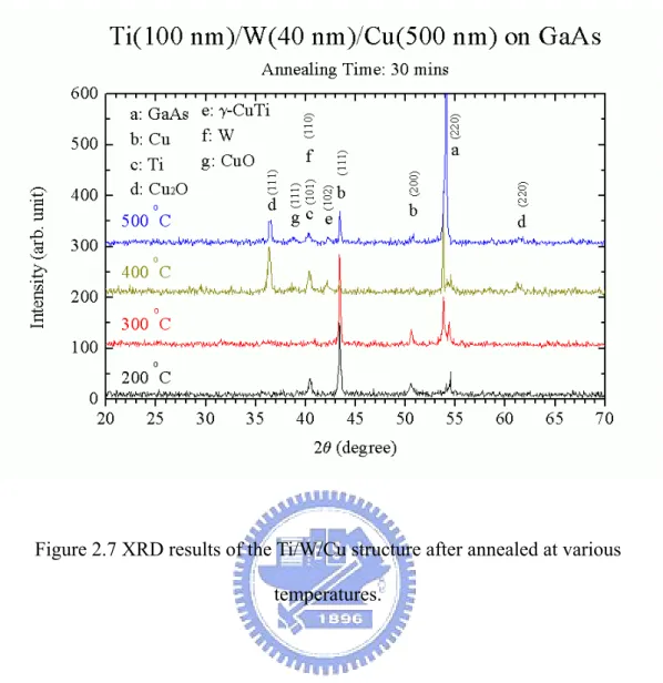
(27) (100) GaAs with thickness of 1µm and concentration of 2.09x1017 cm-3 was used for the fabrication of Ti/W/Cu, Ti/Mo/Cu, and Ti/Co/Cu Schottky diodes. The area of the diode is 3.14 mm2. The Ge/Au/Ni/Au ohmic metals were deposited by the electron beam evaporator and annealed by rapid thermal annealing system (RTA) at 400 °C for 60 sec. The Schottky metals were deposited by sequentially DC sputtering the Ti (1000 Å), barrier layer (= W, Co and Mo) (400 Å), and Cu (5000 Å) targets through a metal mask. The conventional Ti/Pt/Au Schottky diode was also prepared for comparison.. 2.3 X-ray Diffraction Patterns (XRD). Glancing angle X-Ray Diffraction (XRD) with Cu Kα radiation was used to identify the material phases. The annealing treatment was performed at temperatures up to 500 °C for 30 min. Table 2.1 is the summary of XRD analysis results for the structures after annealing at different temperatures from 200 °C to 500 °C for 30 min. The details of these results are described in the following sections.. 2.3.1 The Ti/W/Cu Structure Figure 2.7 shows the XRD patterns of the Ti/W/Cu structure. This results show that the Ti/W/Cu structure was stable after annealing at 300 °C for 30 min. However, there were compounds formed after the 30 min annealing at the temperature higher than 400 °C. CuTi phase formed at 400 °C and 500 °C due to the failure of W as the diffusion barrier for Cu. According to these results, it can be concluded that the W thin film is an effective diffusion barrier layer for Cu at annealing temperature up to 300 °C.. 27.
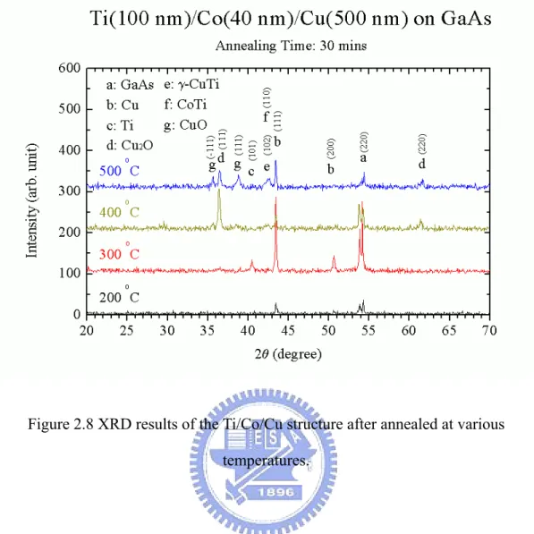
(28) 2.3.2 The Ti/Co/Cu Structure Figure 2.8 shows the XRD patterns of the Ti/Co/Cu structure. This results show that the Ti/Co/Cu structure was stable after annealing at 300 °C for 30 min. However, there was compounds formed after the 30 min annealing at the temperature higher than 400 °C. Co started to react with Ti and formed the CoTi phase at 400 °C and 500 °C. According to these results, it can be concluded that the Co thin film is an effective diffusion barrier layer for Cu at annealing temperature up to 300 °C.. 2.3.3 The Ti/Mo/Cu Structure Figure 2.9 shows the XRD patterns of the Ti/Mo/Cu structure. This results show that the Ti/Mo/Cu structure was thermally stable after annealing at 300 °C for 30 min. However, there were compounds formed after the 30 mins annealing at the temperature higher than 400 °C. CuTi phase formed at 400 °C and the peaks of Cu3Ti were found in the XRD patterns after 500 °C annealing. The formation of these intermetallic compounds was due to the failure of Mo as the diffusion barrier. According to these results, it can be concluded that the Mo thin film is an effective diffusion barrier layer for Cu at annealing temperature up to 300 °C.. 2.4 Measurement and Characterization. Figure 2.10 shows the I-V characteristics of the Schottky diodes with Ti/Mo/Cu, Ti/Co/Cu and Ti/W/Cu, structures as deposited and after annealing at 200 °C for 2 min. Applying thermionic emission theory and considering series resistance, the I-V characteristic of the Schottky diode can be expressed as:. 28. J. =. J. 0. ⎡ ⎛ q (V − JRAeff ⎢ exp ⎜⎜ nkT ⎝ ⎣. )⎞ ⎤ ⎟⎟ − 1⎥. ⎠ ⎦.
(29) 2.1. where saturation current density J0=A*T2exp(-qΦb /kT), q is the electron charge, V is the applied voltage, R is the series resistance, Aeff is the effective area of the Schottky diode, k is the Boltzman constant, T is the absolute temperature, A* is the effective Richardson constant of 8.0375 A cm-2K-2 for GaAs, Φb is the barrier height and n is the ideality factor. All the ideality factors and barrier heights were calculated within the current range of 0.01mA/mm2 to 0.0001mA/mm2. Before the annealing treatment, the ideality factors and barrier height were 1.11/0.76 eV, 1.15/0.78 eV, 1.11/0.7 eV and 1.11/0.77 eV; after annealing at 200 °C for 2 min, the values became 1.09/0.77 eV, 1.05/0.92eV, 1.12/0.73 eV and 1.05/0.69 eV for Ti/Pt/Au, Ti/Co/Cu and Ti/Mo/Cu, Ti/W/Cu structures, respectively. The ideality factor and the Schottky barrier height remained fairly stable after annealing at 200 °C for each structure. The barrier heights after annealing fell in the range of 0.7 eV to 0.9 eV, which is in the same range as the data reported by Seghal [2]. As shown in Figure 2.11, for each diode structure at the same applied forward voltage, the diode current decreased after annealing at 200 °C for 2 min. The Ti/Co/Cu structure shows the most serious degradation (59.0 % at 0.7 V), whereas the Ti/W/Cu structure has little change in current (17.2 % at 0.7 V) after annealing treatment. The different characteristics of the I-V curves for each Schottky diode are due to the different material structures and the related series resistances of the diodes. In order to extract the series resistance of each diode from the I-V curve, a method proposed by Cheung [3] is used. Rearranging and differentiating Eq. 2.1, we can obtain d (V ) nkT = RAeff J + . d (ln J ) q. 2.1 29.
(30) The slope of the line of d(V)/d(lnJ) vs. J is equal to RAeff. Thus, we can easily determine R by Eq. (2). Figure 2.8 shows the plot of d(V)/d(lnJ) vs. J of the Schottky diodes. The series resistances calculated are 39.92 Ω, 43.72 Ω, 57.41 Ω and 60.74 Ω. for Ti/Co/Cu, Ti/Mo/Cu, Ti/W/Cu and Ti/Pt/Au as-deposited structures,. respectively. From the data of the resistance, all the three Cu-metallized Schottky structures have lower series resistance than the conventionally used Ti/Pt/Au structure.. 30.
(31) REFERENCE. 1 Massalski T. B., and Thaddeus B.: ‘Binary phase diagrams’, Metals Park, Ohio, 1986. 2 Sehgal B.K., Gulati R., Naik A. A., Vinayak S., Rawal D.S. and Sharma H. S.: ‘(n)GaAs/Ti/Pt/Au Schottky contacts and their effect on MESFET’s dc parameters’, Materials Sci. Eng., B48, 229(1997) 3. Cheung S. K., and Cheung N. W.: ‘Extraction of Schottky diode parameters from forward current-voltage characteristics’; Appl. Phys. Lett. 49, 85(1986).. 31.
(32) TABLES. Schottky structure Ti/W/Cu. Ti/Mo/Cu. Ti/Co/Cu. 200. Stable. Stable. Stable. 300. Stable. Stable. Stable. Intermetallic. Intermetallic. Intermetallic. compounds formed. compounds formed. compounds formed. Intermetallic. Intermetallic. Intermetallic. compounds formed. compounds formed. compounds formed. Annealing Temperature (°C). 400. 500. Table 2.1 Summary of the XRD results for Ti/W/Cu, Ti/Mo/Cu and Ti/Co/Cu Schottky structures after annealing at 200 °C ~500 °C for 30 min.. 32.
(33) FIGURES. Figure 2.1 Cu/W phase diagram. [1]. 33.
(34) Figure 2.2 Cu/Co phase diagram.[1]. 34.
(35) Figure 2.3 Cu/Mo phase diagram. [1]. 35.
(36) Figure 2.4 Ti/W phase diagram. [1]. 36.
(37) Figure 2.5 Ti/Mo phase diagram. [1]. 37.
(38) Figure 2.6 Ti/Co phase diagram. [1]. 38.
(39) Figure 2.7 XRD results of the Ti/W/Cu structure after annealed at various temperatures.. 39.
(40) Figure 2.8 XRD results of the Ti/Co/Cu structure after annealed at various temperatures.. 40.
(41) Figure 2.9 XRD results of the Ti/Mo/Cu structure after annealed at various temperatures.. 41.
(42) 2. Current Density, J (mA/mm ). 1. 0.1. 0.01. 1E-3. 1E-4 0.0. 0.2. 0.4. 0.6. 0.8. 1.0. Forward Voltage, V (V). Figure 2.10 Forward I-V characteristics of Ti/W/Cu, Ti/Mo/Cu and Ti/Co/Cu structures as deposited and after annealing at 200 ℃ for 2 min ──○── Ti/Co/Cu (as deposited) ──□── Ti/Mo/Cu (as deposited) ──△── Ti/W/Cu (as deposited) ──●── Ti/Co/Cu (annealing at 200℃, 2min) ──■── Ti/Mo/Cu (annealing at 200℃, 2min) ──▲── Ti/W/Cu (annealing at 200℃, 2min). 42.
(43) 0.7. d(V)/d(lnJ) (V). 0.6 0.5 0.4 0.3 0.2 0.1 0.0 0.0. 0.5. 1.0. 1.5. 2.0. 2.5. 3.0. 2. J(mA/ mm). Figure 2.11 Plot of d(V)/d(lnJ) vs. J. The series resistances of the Ti/W/Cu, Ti/Mo/Cu, Ti/Co/Cu and Ti/Pt/Au Schottky structures is proportional to the slope of the fitted line ──◆── Ti/Pt/Au (as deposited) ──△── Ti/W/Cu (as deposited) ──□── Ti/Mo/Cu (as deposited) ──○── Ti/Co/Cu (as deposited) ───── Linear fitting. 43.
(44) Chapter 3 Fabrication of Low Noise GaAs PHEMT. 3.1 Pseudomorphic High Electron Mobility Transistor (PHEMT) Device Structure. PHEMT was used to evaluate the feasibility of using the Cu metallized airbridges as the interconnect metal for GaAs-based devices. AlGaAs/GaAs HEMTs were used in microwave and millimeter-wave low noise amplifier due to their superior noise performance at these frequencies in 1980’s [1]. However, AlGaAs/GaAs HEMTs suffer from a low current level due to the limited sheet concentration which is lower than 1012 cm-2 and lower electron transportation characteristics. At the late 1980’s, AlGaAs/InGaAs pseudomorphic HEMT with better performance was used to replace AlGaAs/GaAs HEMT as the major device used for low noise application. The larger band discontinuity and better transport characteristics in AlGaAs/InGaAs system result in higher two-dimension electron gas (2DEG) concentration with higher electron mobility and current density. In this study, the AlGaAs/InGaAs low noise PHEMT was used and the device was grown by molecular beam epitaxy (MBE) on a 3-inch (100) oriented semi-insulating GaAs substrate. The structure is as shown in Figure 3.1. The epi-layers of the device, from the bottom to the top, are composed of a 600nm buffer, a 15nm InGaAs channel, a 2nm undoped AlGaAs spacer, a 42nm Si-doped AlGaAs donor layer and a 45nm Si-doped GaAs capping layer.. 3.2 Device Process Flow. 44.
(45) The following process flow was used to fabricate PHEMT used in this study. 1. Device Isolation (Section 3.3) 2. Ohmic contact formatin (Section 3.4) 3. Gate formation (Section 3.5) 4. Device passivation (Section 3.6) Device passivation was followed by airbridge process. Airbridge process is not included in this flow and will be described in the following chapter.. 3.3 Device Isolation. Device isolation is the first step for the PHEMT device process. There are three principal ways used to achieve device isolation: mesa etching, ion bombardment, and selective implantation [2]. In this study, mesa etching was used as the device isolation process. Isolation confines the electrically conductive portion of the wafer to specific areas and restricts the current flow in the undesired areas. For the discrete devices such as the LN-PHEMT used in this study, this usually means that the bonding pads are formed on “inactive” electrically insulating areas. Device fabrication started from the mesa isolation using wet etching to remove the materials from the undesired areas and form the active device mesas. This process was performed by immersion etching of the undesired areas in the HF-based solution. The active areas were masked by Shipley S1818 photo resist. The inactive areas were etched to the undoped GaAs buffer layer to provide the isolation between devices. In order to avoid the photo resist peeling during the etching of HF-based solution, the wafer surface was pre-treated before resist coating by Hexamethyldisilazane (HMDS) vapor at 150°C for 3 minutes and 30 seconds to improve the resist adhesion on the 45.
(46) substrate. The cross-section of the substrate after mesa isolation is shown in Figure 3.2a.. 3.4 Ohmic Contact. There are two kinds of metal contacts on the PHEMT: one is ohmic contact, which forms the source and the drain electrodes, and the other is Schottky contact, which forms the gate electrode. The ohmic contact should have a linear I-V characteristic with a resistance as small as possible, and should be thermally stable. The patterning of the ohmic metal depends on the photolithography process. Although lithography techniques are quite mature in Si industry, lithography process in GaAs processing is quite different. There are two basic metal patterning process: one is the metal etch mask process typically used in Si process. The other is the lift-off process commonly used in GaAs industry. There are some reasons for such difference. Firstly, GaAs substrate will be attacked by many metal etchants. Secondly, aluminum, which can be easily etched in relatively innocuous etchant and can also be easiliy etched by dry etch techniques, is used by Si processing as the metallization metal. Meanwhile, GaAs uses AuGeNi as Ohmic metal and TiPtAu as Schottky metal. These composite metal systems cannot be easily etched by a simple solution or dry etch techniques. In this study, lift-off process was also used for the Ohmic and Schottky metallization processes. Karl Suss MJB3 contact aligner with xenon-mercury lamps was used as the photolithography equipment for the patterning of Ohmic metals. Xenon-mercury lamp emits deep ultraviolet (DUV) light with the wavelength in the 220-240 nm range. Glass is highly absorptive at these wavelengths, so quartz masks were employed. In this work, polymethylmethacrylate (PMMA) and its copolymer with polymethacrylic 46.
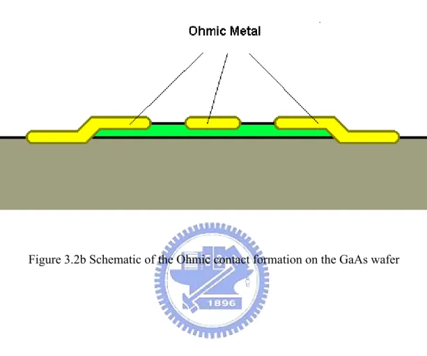
(47) acid (PMAA) were used as the resists for the lift-off process. The lift-off process is illustrated in Figure 3.3. The copolymer of PMMA-PMAA was coated on the substrate firstly and then baked at hot plate at 120 °C for 90 seconds. PMMA was subsequently coated and the wafer was again hotplate-baked at 170 °C for 90 seconds. The resist is then exposed by DUV light source. Because the different light sensitivities of PMMA and PMMA-PMAA, the remaining resists formed lift off profile after exposure and development. HCl-based solution was used as the pre-metallization cleaning solution to remove the native oxide of the GaAs surface before Ohmic metallization. The Ohmic metals used were Au/Ge/Ni/Au. After metal deposition, the resist was lifted off and Ohmic metals were formed at the desired areas. The most common method of forming Ohmic contacts on n-type GaAs is to apply an appropriate metallization scheme to the heavily doped GaAs followed by annealing process. During the annealing process, one of the constituent metals diffuses into the wafer and dopes the cap GaAs layer heavily. Many kinds of alloying systems for n-type ohmic contacts have been studied in literature. In this study, AuGe alloys were used to form the Ohmic contacts. The Ohmic metals deposited, from the bottom to the top, were Au, germanium, nickel and Au. In the study, germanium atoms diffused into the GaAs and heavily doped GaAs during the thermal annealing process. The Au on the top is usually quite thick, this is for reducing the sheet resistance of the electrodes. After the AuGeNiAu metallization, the contact resistance was measured by using transmission line model (TLM). The optimized conditions for thermal alloying is 400 °C for 30sec by rapid thermal annealing (RTA) method. The cross-section of the Ohmic metallization after thermal treatment is shown in Figure 3.2b.. 47.
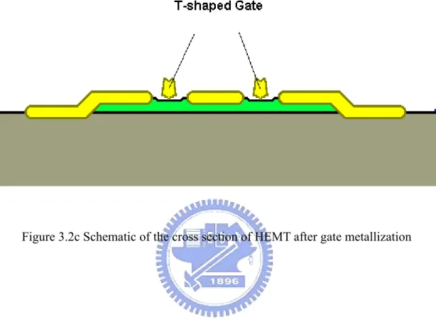
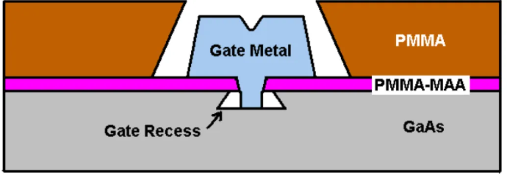
(48) 3.5 Gate Formation. Short gate length with low gate resistance is desirable for HEMTs for high frequency and high speed applications. The most common approach for obtaining low gate resistance is the use of T-shaped gate structure. For T-gate structure, the small footprint defines the gate length and the wide top provides a low gate resistance. T-shaped gates were achieved by using a multilayer resist technique with E-beam lithography. In this study, PMMA/PMMA(MAA) were used as the resist system to form the T-shaped gates. The fabricated PHEMT in this study has a gate length of 0.25 µm. After the gate resist development, the exposed HEMT channel was recessed to achieve the desired channel current and pinch-off voltage characteristics. That means a groove is fabricated in the exposed surface of the wafer to “recess” the gate. This process is done by wet etch technique in this study, although dry etching methods may also be used. The schematic of the HEMT with recessed gate is as shown in Figure 3.4. The gate recess profile in this study was achieved by using e-beam lithography. In such case, the opening in the PMMA-MAA layer determines the gate length; the opening of the top PMMA layer determines the width of the top portion of the T-shaped gate. The method used to control the recess depth is to monitor the source-to-drain current during the etching process. For low noise PHEMT, the saturation current and the slope of the linear region go down as the recess groove was etched deeper and deeper. The concentration of the etchant should be adjusted to provide an etch rate that is sufficiently slow to allow good control over the recess process, thus enable the operation to approach the target current value, without overetching it. Several recess etchants were considered and tried. However, citric acid/hydrogen peroxide solution 48.
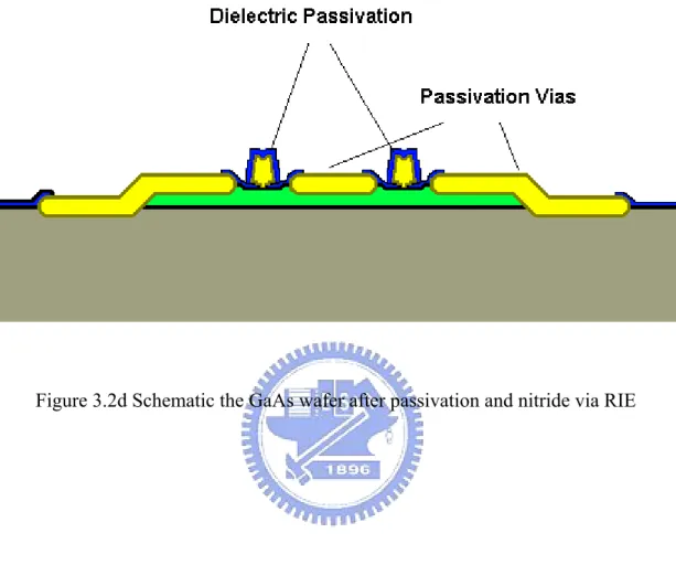
(49) was used because of the good process control. The wet etchant usually leaves a thin oxide on the GaAs. HCl-based solution was used to remove the surface oxide. After gate recess process, the wafer was cleaned in the solution of HCl:H2O=1:10 solution to remove the native oxide formed on the exposed wafer surface, and the gate metal Ti/Pt/Au was evaporated by E-gun evaporation. After the gate metal was formed, DC characteristics were measured. The cross-section of the HEMT after gate metallization and lift-off process is as shown in Figure 3.2c.. 3.6 Device Passivation. Plasma enhanced chemical vapor deposition (PECVD) nitride was used on the sample for surface encapsulation. The major purpose of the silicon nitride protective encapsulation is simply for the surface passivation. This passivation protects the critical area of the originally exposed wafer surface from humidity, chemicals, gases, and particles. The reason why silicon dioxide was not used as the passivation dielectrics in this study is that silicon nitride is less permeable to ions than silicon dioxide, therefore the silicon nitride is relatively reliable material for device passivation. In this study, Samco PECVD system was used for depositing silicon nitride film. The processing gases of passivation PECVD were Silane, ammonia, and nitrogen. The process condition is: process pressure: 100Pa, process temperature: 250 °C and process time: 6 minutes and 30 seconds. Passivation Vias between Au contacts and airbridge interconnects were etched by reactive ionic etcher (RIE). This process used the Plasmatherm RIE system and the etching condition was: gas pressure: 60 mT, RF power: 50 W, etching gases: CF4/O2, process time: 1 minute and 40 seconds and the etching depth: 1000 Å film. The DC 49.
(50) performances of the unfinished device with single gate finger were measured by HP4142 for preliminary device evaluation before the interconnect process. The schematic of the device after passivation and via opening is as shown in Figure 3.2d.. 50.
(51) REFERENCE. 1. Fazal Ali, Aditya Gupta: HEMTs and HBTs: Device Fabrication, and Circuits, Artech House, Boston, London, 1991. 2. Ralph Williams, Modern GaAs Processing Methods, Artech House, Norwood, MA, 1990.. 51.
(52) FIGURES. Figure 3.1 Structure of the AlGaAs/GaAs LN-PHEMT. 52.
(53) Figure 3.2a Schematic of the wafer after mesa isolation.. 53.
(54) Figure 3.2b Schematic of the Ohmic contact formation on the GaAs wafer. 54.
(55) Figure 3.2c Schematic of the cross section of HEMT after gate metallization. 55.
(56) Figure 3.2d Schematic the GaAs wafer after passivation and nitride via RIE. 56.
(57) Figure 3.3 Schematic of the lift-off process for ohmic metallization formation.. 57.
(58) Figure 3.4 Schematic of the HEMT after recess and gate deposition, but before PMMA/PMMA-MAA lift off.. 58.
(59) Chapter 4 Technology Development of the Cu-Metallized Airbridges. 4.1 Overview. A metal interconnects with air between the metal interconnect and the wafer surface beneath is called an airbridge. Airbridges are used extensively in GaAs analog devices and MMICs for interconnections [1]. They may be used to interconnect sources of FETs, to cross over a lower level of metallization, or to connect the top plate of a MIM capacitor to adjacent metallization. The airbridges have several advantages including low parasitic capacitance, and the ability to carry substantial currents if the plated airbridge is thick enough. Analog GaAs devices operating at high current density benefit from airbridges with thick plated metal layer. Low parasitic capacitance (between the bridge and any metallization beneath) follows from the large spacing and low dielectric constant of the intervening medium. The capacitance is a function of the thickness, and the dielectric constant of the intervening material. Air (k=1.0) has a much lower dielectric constant than any other dielectric, and the space under the airbridge tends to be greater than the thickness of typical dielectrics. These considerations mean that airbridge crossovers are less capacitive than the dielectric type by a factor (typically) of five to twenty. Traditionally, Au is used as the interconnect metal in III-V device fabrications, mainly owing to its high electrical conductivity and better chemical inertness with no surface oxidation. Recently Cu has been used widely in Si IC interconnects due to its low resistivity and high electromigration resistance. Both the resistivity and the material cost of Cu (1.67 µΩ-cm) are lower than those of Au (2.2 µΩ-cm). Based on 59.
(60) the above advangages, Cu were used instead of Au as the airbridge metal in order to provide better thermal and electrical conductivities for the device applications.. 4.2 Comparison between Au Airbridge and Cu Airbridge Processes. The process flow of airbridges used in this study is as shown in Figure 4.1. There are three main differences between the fabrications of Au airbridges and Cu airbridges: thin metal structure, electroplating and airbridge passivation. Ti/Au/Ti structure is widely used as thin metals of Au airbridge interconnect in conventional GaAs MMIC industry. Ti layers are used as the adhesion layer between Au and photo resist. Besides, the top Ti layer confines the electroplating area and thus prevents the electroplated Au from intruding into the areas that is originally covered by photo resist. The Au layer between two Ti layers is used as the seed layer for Au electroplating. The thin metals used for Cu-metallized airbridges on Au contacted PHEMT must prevent Cu atoms from diffusing into the Au layer. On the other hand, the adhesion of such metal system must be good enough to prevent metal peelings. Finally, Cu-metallized PHEMTs that use such a thin metal structure must have comparable, or even better electrical performance compared with the Au-metallized PHEMTs. The seed layers for electroplating of these two airbridges are different. Evaporated Au was used as the seed layer for electroplated Au whereas the electroplated Cu used sputtered Cu as the seed metal. Cyanide-based solution was used for Au electroplating in this study. The environment of Au electroplating is tough on photo resist because the process temperature is up to 65 °C, which may has the risk for suffering photo resist deformation and dissolution in the electroplating solution. Compared to Au electroplating, Cu electroplating has several advantages. Cu 60.
(61) electroplating is less expensive, less toxic than the cyanide-based electroplating of Au. Cu electroplating of sulfuric acid system can be done at room temperature. Therefore, the photo resist can sustain of a longer process time in Cu electroplating solution than in Au electroplating solution.. 4.3 Thin Metal Structure Used for Cu Airbridges on PHEMTs fabricated with Au-Metallized Contacts. Cu is one of the most common unintentional impurities in semiconductor including GaAs. It diffuses rapidly at low temperatures by interstitial diffusion process [2]. In GaAs, Cu tends to getter on to crystalline defects and acts as a double acceptor, being incorporated at a substutional lattice site as a CuGa [3]. Au used in microelectronics is highly pure, usually 99.99% or better. One reason for the requirement of high purity Au is the rapid increase in electrical resistance as a function of impurity concentration. According to the study of Reid [4] in 1974, the resistivity of pure Au is 2.2 µΩ/cm. However, 1 at. % of Cu alloyed with Au increases the resistivity up to 3.59 µΩ/cm, which is 63.3 % greater than that of pure Au! Based on these well-known characteristics, Cu is traditionally regarded as harmful to GaAs material and devices. No Cu contaminations to either GaAs or Au are allowed in the traditional PHEMT fabrication. In this study, Cu replaced Au as the metal for airbridge interconnects. In order to avoid the interatomic diffusion of Cu and Au, the diffusion barrier used in this study must be thermally stable to protect the PHEMTs with Au contacts from the Cu diffusion. From the experiences of Si industry, refractory metal and their nitride could be used as the diffusion barrier to prevent the Cu diffusion into the underlying devices. 61.
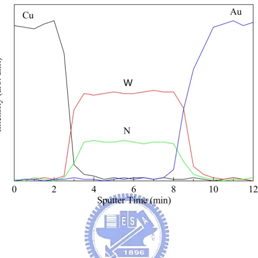
(62) The detailed introductions of these refractory metals as the diffusion barriers have been described in Chapter 1. Most of these metal nitrides are thermally stable under the normal operation of GaAs devices. Among these materials, WNx was chosen as the diffusion barrier of Cu metallization upon GaAs PHEMT because of the feasibility of process integration. WNx can be etched by several chemical solutions such as hydrogen peroxide and acid-hydrogen peroxide solution. These solutions were widely used in the fabrication of GaAs devices.. 4.3.1 Materials study of WNx as the Diffusion Barrier In this study, the thermal stabilities of the thin metal systems WNx/Cu on Au were studied. 400 Å WNx and 1000 Å Cu were sputtered upon the Au layer on the GaAs blanket wafers. These wafers were subsequently splitted up to four groups. Three of them were separately annealed at 350 °C, 400 °C and 450 °C for 30 minutes under nitrogen atmosphere. Auger Electron Spectroscopy (AES) and X-ray Diffraction Pattern (XRD) were then used for materials analysis of all these four different kinds of samples.. 4.3.1.1 AES Depth Profile Auger Electron Spectroscopy (AES) was used to analyze the depth profiles of Au/WNx/Cu multilayer system. The data acquisition of AES depth profile analysis combines ion beam sputtering yielding in-depth element information. Figure 4.2a~d show the AES depth profiles of the Au/WNx/Cu multilayer system annealed at different temperatures. From the results of these profiles, the diffusion barrier WNx was thermally stable even up to 350 °C annealing for 30 minutes. When the annealing temperature was 400 °C, the profile of WNx remained changed and the Cu began to diffuse into the WNx layer. Suh [5] 62.
(63) suggested that amorphous WNx films with nitrogen contents of less than 18% would recrystallize when the annealing temperature was up to 450 °C, as shown in Figure 4.3. Interestingly, when the temperature was up to 450 °C, there was still little Cu in WNx but lots of Cu atoms had penetrated WNx and accumulated in the Au layer. The reason why very few Cu atoms were found in WNx could be that the W can dissolve a large amount of Cu atoms at 450 °C but have only limited solubility for Cu atoms at room temperature. When the temperature was increased to 450 °C, Cu atoms penetrate the tungsten nitride layer into the underlying Au layer. However, after the annealing temperatures were slowly decreased to room temperature, Cu atoms which were originally at the tungsten grain boundaries diffused out of the WNx layer into the Au layer because of the limited Cu solubility in the tungsten nitride at room temperature.. 4.3.1.2 X-ray Diffraction Patterns (XRD) X-ray diffraction (XRD) patterns were used to analyze the structures of the Au/WNx/Cu multilayer system after thermal annealing. The XRD patterns of this material system before and after thermal annealing are shown in Figure 4.4. When the annealing temperature was up to 450 °C, Cu started to diffuse into Au layer and formed intermetallic compounds.. 4.3.1.3 Summary of the Materials study of WNx/Cu on Au Compared the XRD patterns and the AES depth profiles, it can be concluded that the generation of these intermetallic compounds was due to that Cu atoms diffused through the WNx layer and formed several kinds of intermetallic compound with Au atoms. These intermetallic compounds have higher resistance than Cu and Au, which impact the RF performance of the 63.
(64) LN-PHEMT. Although there’s no obvious intermetallic compounds formed after 400 °C annealing from the XRD patterns, there exists a certain risk of interatomic diffusions because the AES depth profiles of the Cu and Au atoms showed that Cu and Au atoms started to diffuse into the WNx layer at such a temperature. From the results of XRD and Auger analysis, it can be concluded that WNx was still a good diffusion barrier between Cu and Au even after 350 °C annealing for 30 minutes under nitrogen atmosphere.. 4.3.2 Adhesion Layer At the initial stage of this study, 400 Å WNx and 1000 Å Cu were used as the diffusion barrier for the fabrication of Cu-airbridged GaAs PHEMTs. However, the problems of electroplated-Cu peelings were observed during the airbridge process and the RF measurement. The electrical characteristics of GaAs PHEMTs with WNx/Cu as the thin metal structure also showed an inferior uniformity. Figure 4.5 shows the metal peeling after RF probing and two different colors were observed at the peeling areas on the GaAs PHEMTs. The metal contacts revealed golden color. The color of the areas of nitride, which were originally covered by electroplated Cu, was brown. The nitride areas without any material covering upon it after airbridge process showed the color of light yellow. According to the inspection of this failure, the peeling structure was depicted schematically in Figure 4.6. It seemed that metals peeled between Au and WNx at the area of metal contacts while the peeling occurred between WNx and Cu at the areas of silicon nitride. Based on this assumption, it is necessary to improve the adhesion of WNx on Au and Cu on WNx for the Cu airbridge process. The Ti/WNx/Ti/Cu multilayer system was used as the thin metal of Cu 64.
(65) airbridges to overcome the metal peeling issues. Two Ti layers of 300 Å thick were added separately under and upon the WNx layer to improve the adhesions. Ti was widely used as the adhesion layer in the semiconductor industry. The adhesion characteristics of Ti were introduced in Chapter 1. Ti was also used in the fabrication of conventional Au airbridges and it can be etched by the diluted hydrogen fluoride solution. The deposition and etching processes of Ti are compatible with the conventional process used in GaAs device fabrications. Metal peelings no longer occurred on the GaAs PHEMTs fabricated with Ti/WNx/Ti/Cu. GaAs PHEMTs fabricated with different thin metal systems were sampled and the uniformities of the DC characteristics of these devices are as shown in Figure 4.7 and Figure 4.8. The average transconductance of the devices using Ti/WNx/Ti/Cu as thin metals were greater than those of the devices using WNx/Cu. The standard deviations of Gm and Vp of GaAs PHEMTs fabricated with WNx/Cu were 97 mS/mm and 0.22 V, respectively. The standard deviations of Gm and Vp of GaAs PHEMTs fabricated with Ti/WNx/Ti/Cu were 33 mS/mm and 0.14 V, respectively. GaAs PHEMTs fabricated Ti/WNx/Ti/Cu showed better uniformity in Gm and Vp than HEMT fabricated with WNx/Cu layers. The improvement on the RF performance was due to the additional adhesion layers as shown in the following chapter.. 4.3.3 Thin Metal Etching The etching selectivity of the thin metal determines the airbridge profile and metal thickness. Appropriate etchants should be chosen so that these etchants won’t overetch the airbridge metal. In the conventional Au airbridge process, KI solution is used to etch the Au layer of the thin metal structure and HF solution is used to etch the Ti layers. The thickness of the thin metal Au is only 500 Å, which is much 65.
(66) thinner than 2 µm-thick electroplated Au. Au doesn’t react with HF solution. After the thin metal etching, the thickness of the electroplated Au doesn’t change too much and remains about 2 µm. Figure 4.9 shows the SEM photograph of the Au airbridges after thin metal etching. Several etchants were chosen to etch the thin metals of the Cu airbridge. NH4OH: H2O2: H2O solution can etch both WNx and Cu and was used as the non-selective etchant of the WNx/Cu metal structure. However, the Cu etching rate is much greater than the WNx etching rate. After the thin metal etch, the Cu airbridge was seriously damaged and there were still some WNx protruding at the edges of the airbridge as shown in Figure 4.10. These WNx protrudings cause the risk of metal short and also the resistive loss of the RF performance. In order to improve the Cu airbridge profile after thin metal etching, it is necessary to develop the selective etching process to remove the thin metals. In this study, the selective etching was used to etch the Ti/WNx/Ti/Cu multilayer system. The thin Cu metal was etched by H2SO4/H2O2/H2O solution mixed in the volume ratio of 5:6:100. Diluted HF solution was used to etch Ti layers and diluted H2O2 solution was used to etch WNx layer. Diluted HF solution without mixing with other chemicals didn’t etch Cu too much. Although H2O2 solution oxidized the Cu surface, the oxidation was only on the surface. After WNx was etched in the H2O2 solution, HF solution was used to etch the bottom Ti layer and simultaneously removed the surface oxide of the Cu airbridge. Figure 4.11 shows the SEM photograph of the Cu airbridges after the selective thin metal etching, the bridge metal was not seriously etched and no metal protrudings were observed.. 4.4 Cu Electroplating 66.
數據
+7

相關文件
a single instruction.. Thus, the operand can be modified before it can be modified before it is used. Useful for fast multipliation and dealing p g with lists, table and other
• 接續之前的例子,若原為 0.288 pF 的液晶 電容 C LC ,再並聯一個亦為 0.288 pF 的電 容C st ,則電位保持的變化值為.
We do it by reducing the first order system to a vectorial Schr¨ odinger type equation containing conductivity coefficient in matrix potential coefficient as in [3], [13] and use
Results for such increasing stability phenomena in the inverse source problems for the acoustic, electromagnetic, and elastic waves can be found in [ABF02, BLT10, BHKY18, BLZ20,
The hashCode method for a given class can be used to test for object equality and object inequality for that class. The hashCode method is used by the java.util.SortedSet
How would this task help students see how to adjust their learning practices in order to improve?..
Students should also be able to appreciate the interrelation between bonding, structures and properties of substances by learning the properties of metals, giant ionic
The nanostructure with anisotropic transmission characteristics on ITO films induced by fs laser can be used for the alignment layer , polarizer and conducting layer in LCD cell.
