Efficiency Enhancement in Dye-Sensitized Solar Cells Fabricated with
Nanostructured Thin Film
Feng-Chyi Duh1, Chih-Chou Chang2, Jen-Lung Lo3
1 Department of Mechatronics Engineering, Ta Hwa Institute of Technology 2 Industrial Technology Research Institute
3 Department of Computer Science and Information Engineering, Ta Hwa Institute of Technology Correspondence author email:E-mail: [email protected]
Abstract
To increase the photoelectric conversion efficiency of dye-sensitized solar cells (DSSCs), nanostructured fabrications were used to enhance the absorption of incidence light. In the current study, we measured the characteristics of DSSCs by fabricating a thin layer of titanium dioxide (TiO2), an antireflection film, a scattering layer, and a reflection film. The first fabrication involved printing TiO2 paste on the glass of a working electrode to form a nanoporous layer 13.5–19.5 μm thick and containing TiO2 particles with radii of approximately 10–20 nm. The second fabrication adopted argentum nanopowder as an antireflection film, with a 97% reflection ratio at a 650 nm wavelength. The third fabrication utilized particle radii of approximately 100–400 nm to be used as a scattering layer. In the final fabrication, the antireflection film employed in the experiment increased the transmittance of solar cells up to 2%–3% at a wavelength of 350–900 nm. The best photoelectric conversion efficiency of 6.5% for a 70.92 cm2 DSSC was obtained using nanostructured thin film fabrication.
Keywords – Titanium dioxide layer (TiO2), Antireflection film, Reflection film, Scattering layers
1. Introduction
Dye-sensitized nanocrystalline solar cells (DSSCs) were discovered in 1960, creating a new research and development field in solar cells. DSSC technology was developed by Grätzel at Ecole Polytechnique Federale de Lausanne (EPFL) in the 1990s, showing great promise as a cheap alternative to expensive silicon solar cells. DSSCs imitate the way plants and certain algae convert sunlight into energy. The cells comprise a porous film of nanostructured white pigment particles of titanium dioxide (TiO2). In 1991, the DSSC had significant progress because of the development in nanotechnology. Since then, it has become the focus of new renewable energy studies in many countries around the globe [1, 2]. Under standard test conditions, the value of the photoelectric conversion efficiency of DSSC is presently up to 11.5% [3, 4].
The structures of DSSCs and normal photovoltaic cells are different [5, 6]. The substrates of DSSCs are glass or transparent flexible polymer foil. A layer of transparent conducting oxide (TCO), usually using fluorine-doped tin oxide (FTO, SnO2:F), is fabricated on glass to form a nanoporous layer approximately 10 μm thick and containing titanium dioxide (TiO2) particles with radii of approximately 10–20 nm. Then, another layer of dye is fabricated by TiO2 particles. Normally, the organic dye is a complex containing ruthenium (Ru) ions. The top electrode utilizes glass and TCO plated with a layer of platinum as a catalyst for electrolyte reaction. The electrolyte is poured into the space between the two electrodes.
Basically, a DSSC utilizes metal-oxide-semiconductor particles [7] to absorb dye molecules on its surface ©2007 National Kaohsiung University of Applied Sciences, ISSN 1813-3851
through chemical method. The DSSC then utilizes these molecules on the anode in a cell circuit as a photoreceptor layer. An electrolyte layer is added between the photoreceptor layer and cathode to induce an oxidation-reduction reaction in the cells [8]. Nanometals have special photon characteristics; the sludge of the nanometal on the semiconductor material is able to considerably improve the efficiency of the catalytic reaction in a sensitized dye [9]. The fabrication principle of the DSSC module uses thin layers of TiO2 that are plated on the substrates layer by layer. In nanotechnology, depositing molecules and atoms on a thin layer takes time; simultaneously using the design of current collection to allow the module to capture more light and to generate electric power is also time consuming.
According to the research results of Yamaguchi et al. [10], the efficiency of a plastic substrate DSSC with an area of 0.25 cm2 could be up to 8% under illumination at 100 mW/cm2. Under the same illumination condition, the plastic substrate DSSC efficiency with an area of 1.111 cm2 is up to 7.6%. Plastic-substrate DSSC shows great potential; however, its efficiency cannot compare to that of glass-substrate DSSC. The glass substrate DSSC has been developed well, and its theory has matured. Therefore, a continuous development of various new methods to increase the incident photon-to-current conversion efficiency is expected.
According to the work of Kroon et al. [11], in the near-infrared range, sensitized dye has an optimal condition at 800–900 nm. The photocurrent is limited to 15–20 mW/cm2 because light absorption is ineffective. However, the photocurrent could be raised up to above 23 mW/cm2 if the appropriate dye is adopted.
The two sides of the DSSC module are able to absorb light and facilitate the absorption of diffused light. The light source in the room can be used to generate electric power if the photoelectric conversion efficiency is raised effectively. The main reason that DSSC is still not widely used in commercial applications is that the maximum theoretical value of the photoelectric conversion efficiency has not been achieved thus far. Researchers have found that the electron conveyed to the cathode in DSSC is ineffective, and its performance is seriously limited in photovoltaic conversion. Studies on the potential commercial applications of DSSC have found that the TiO2 particle layer for plating should be approximately 10 μm thick for optimal light-absorbing ability. Therefore, improving the value of the photoelectric conversion efficiency is our primary requirement.
2. Experimental Facility and Method
2.1 Facility description
All the experiments in this paper were indoor tests. The sunlight source for the device test was from a solar simulator. The solar simulator characteristics are very important for the indoor test because there is a close relationship between the output efficiency of solar cells and the irradiance light spectrum. To accurately measure the electrical characteristics of solar cells, the light spectra from the solar simulator and from the real sunlight source should be as close as possible.
We used short-circuit current density (Jsc), open-circuit voltage (Voc), fill factor (FF), and photoelectric conversion efficiency (η) to estimate the efficiency of DSSC. Jsc expresses the current value under an unconnected load (as voltage is equal to zero). These parameters can be expressed as follows:
oc sc max V J E = FF (1)
where Emax is the maximum output power density. If the input irradiance is expressed as Ein under the standard test conditions (STC: AG1.5, 1000 W/m2, 25 ℃), then the value of η can be defined as follows:
% 100 × E V × J × FF = % 100 × E E ≣ η in oc sc in max (2)
Therefore, the above measured parameters can be used to calculate the maximum output power (Pmax):
A E =
Pmax max (3)
where A is the active area in solar cells and is defined as irradiance light to the effective surface of DSSC.
3.2 Testing procedures
The tested structure of the DSSC module is shown in Figure 1. We measured the characteristics of the solar cells by fabricating the antireflection film (AR film), the number of the TiO2 thin layers, the scattering layer, and the reflection film (R film). The thickness of the TiO2 electrode will be broken above 23 μm; therefore, the thickness of the working electrode is fabricated on the glass to form a nanoporous layer approximately 13.5–19.5 μm thick and containing TiO2 particles with radii of approximately 10–20 nm.
Figure 1. The tested structure of DSSC module
Towards increasing the efficiency of light absorption, one layer of argentum (Ag) reflection film (97%, 650 nm) was plated on the bottom layer to investigate the effectiveness of increasing the light utilization ratio. Particles with radii of approximately 100–400 nm were applied on the scattering layer to increase the probability of photon absorption in the active layer. Spherical vacant spaces were formed when the particles were applied; therefore, the efficiency of capturing light was enhanced.
In our experiment, the antireflection film was applied on the FTO glass of DSSC to achieve the antireflection effect on the broadband wavelength. After the film was applied, the reflected light was reduced and the percentage of passing through the FTO glass was increased. The antireflection film increased the transmittance of solar cells up to 2%–3% at wavelengths of 350–900 nm.
The current-voltage (I-V) characteristics of the DSSC module were measured using a digital source meter under AM1.5 simulator illumination at 100 mW/cm2. The tested DSSC module was fabricated by the Industrial Technology Research Institute (ITRI) in Taiwan. The actively illuminated area was 70.92 cm2 for all measurements.
3. Results and Discussion
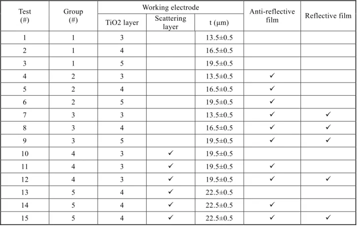
We increased the thickness of the TiO2 layer and added fabricated antireflection film, reflection film, and scattering layer to investigate the effect of DSSC. After a systemized classification, we classified 15 sets of experimental results into 5 groups, as shown in Table 1. Group 1, consisting of Tests 1–3, used the TiO2 thin layer as its fixed factor. Group 2, comprising Tests 4–6, used the TiO2 thin layer and the antireflection film as fixed factors. Group 3, which includes Tests 7–9, used the TiO2 layer, the antireflection film, and the reflection film as fixed factors. Group 4, composed of Tests 10–12, used three layers of TiO2 and one scattering layer as fixed factors and the antireflection and reflection films as variable factors. Group 5, comprising Tests 13–15, used four layers of TiO2 and one scattering layer as fixed factors and the antireflection and reflection films as variable factors. The TiO2 layer of the working electrode consisted of 20 nm nanospherical particles. The active area of the solar cells was 70.92 cm2. The average thickness of the TiO2 layer in each working electrode was 4.5±0.5 μm in the first three layers, and 3.0±0.5 μm from the fourth layer in. In the screen-printing procedure, the thickness of the TiO2 layer was broken at approximately 23 μm. Therefore, the number of layers was limited to five layers (thickness of 22.5 μm).
Table 1 Experimental conditions Working electrode
Test
(#) Group (#) TiO2 layer Scattering
layer t (μm)
Anti-reflective
film Reflective film
1 1 3 13.5±0.5 2 1 4 16.5±0.5 3 1 5 19.5±0.5 4 2 3 13.5±0.5 9 5 2 4 16.5±0.5 9 6 2 5 19.5±0.5 9 7 3 3 13.5±0.5 9 9 8 3 4 16.5±0.5 9 9 9 3 5 19.5±0.5 9 9 10 4 3 9 19.5±0.5 11 4 3 9 19.5±0.5 9 12 4 3 9 19.5±0.5 9 9 13 5 4 9 22.5±0.5 14 5 4 9 22.5±0.5 9 15 5 4 9 22.5±0.5 9 9
As shown in Table 2, the open-circuit voltage (Voc) was slightly reduced once the thickness of the TiO2 layer was increased. The reduced value is comparatively obvious in Group 1, but the decreased breadth was only 2.86%. The decreased value in breadth was only 1.45% both in Groups 2 and 3. However, Voc became fixed at 0.68 V once the thickness of the TiO2 layer became greater than 16.5 μm, as shown in Figure 2. The surface area is much bigger than the area on the substrate because the holes on the TiO2 layer are at nanoscale. Therefore, the TiO2 porous layer can absorb more dyes to capture more light and to substantially increase the value of current.
According to Figure 3, Groups 1 and 2 have a linear relationship. The comparative increasing margin of Jsc is slightly decreased as TiO2 increased, and the margin changed from 3.7% to 2.4%.
In theory, TiO2 has higher light catalytic activity. The FF value of DSSC is better if the thickness of the TiO2 layer is increased. Therefore, the performances of DSSC in Groups 1 and 2 were significantly affected; however, the FF value in Group 3 did not increase, as shown in Figure 4.
Table 2 Experimental results Test
(#) Group (#) (mA/cmJsc 2) Voc (V) FF (-) (%) η (mW) Pout
1 1 11.52 0.70 0.61 4.93 350.42 2 1 12.57 0.68 0.61 5.25 372.37 3 1 13.38 0.68 0.62 5.66 401.70 4 2 11.95 0.69 0.61 5.03 353.87 5 2 12.87 0.68 0.61 5.36 380.36 6 2 13.70 0.68 0.62 5.76 408.30 7 3 12.81 0.69 0.61 5.38 381.57 8 3 13.62 0.68 0.61 5.71 405.30 9 3 14.59 0.68 0.61 6.11 433.41 10 4 14.10 0.70 0.61 6.02 426.65 11 4 14.30 0.70 0.62 6.14 435.60 12 4 14.59 0.70 0.61 6.28 445.36 13 5 14.43 0.70 0.62 6.25 443.50 14 5 14.59 0.70 0.62 6.32 448.15 15 5 14.99 0.70 0.62 6.50 459.95
Figure 3. Jsc vs. t under different conditions of fabricating with nano-structured thin film
Figure 4. FF vs. t under different conditions of fabricating with nano-structured thin film
As shown in Figure 5, the η of DSSC linearly increased with the increase in the thickness of the TiO2 layer. These results are similar to those presented in Yamaguchi’s papers [10, 13]. For an efficient DSSC, the TiO2 layer of the working electrode should provide sufficient surface area for dye absorption and the current path, and have a porous structure to facilitate electrolyte diffusion.
In Section 2, one layer of antireflection film was fabricated on the surface of DSSC to reduce the amount of light reflection and to increase the amount of incidence light. Therefore, the DSSC with antireflection film increased the amount of incidence light by approximately 2%–3% at a wavelength range of 350–900 nm. The main difference between Groups 1 and 2 is that only Group 2 had an antireflection film. Figure 2 reveals that Voc was slightly affected by the thickness of the antireflection film and that Voc is the same when the TiO2 thickness is increased. However, with an antireflection film thickness under 16.5 μm (only 1.43% lower), Voc is reduced in DSSC.
The FF values in Groups 1 and Group 2 are relatively unaffected by the antireflection film (Figure 4). Analyzing the η affected in the quantification data, the two groups revealed linear tendencies that are nearly parallel (see Figure 5). The quantification of differences as the TiO2 thickness increased was near 0.1%.
In Section 3, an argentum antireflection film was attached on the unlit surface. The light passed through a transparent electric conduction glass to the antireflection film. In the visible light range, the best architecture for back-surfaced reflection is the argentum film. Therefore, argentum nanopowder with a reflection ratio of approximately 97% at a 650 nm wavelength was adopted as the antireflection film. The main difference between Group 2 and Group 3 is that Group 3, unlike Group 2, had silver antireflection film. As shown in Figure 2, the values of Voc in Groups 2 and 3 were not affected by the antireflection film at various TiO2 thicknesses. The values of Voc were the same in the two groups when the thickness of TiO2 was 16.5–19.5 μm.
We next compared the different conditions of fabricating with nanostructured thin films. This experimental study considered Groups 1–3. Figure 3 shows the vertical coordinate of the short-circuit current density (Jsc) and the horizontal coordinate of the TiO2 layer thickness (t). The figure shows that Jsc generally increased linearly with t in the three groups. The results show a linear least squares data fit that can be simply expressed by the following correlation:
Jsc = 0.3 t + c1
where the coefficient c1 is a constant. The best fit for the different groups was determined by the least-squares method. The results indicate that under different conditions of fabricating with nanostructured thin films in Groups 1–3, the coefficients of c1 were 7.53, 7.85, and 8.74 mA/cm2, respectively.
The value of FF was not affected by the antireflection, and the quantification data were kept at 0.61, as shown in Figure 4. However, without antireflection, FF showed a slight gradual increase when the TiO2 thickness increased to approximately 16.5 μm. Finally, we analyzed the change in η, which appeared linear and parallel in the three groups, as shown in Figure 5. The antireflection increased the value of the η up to 0.35%. The results show a linear least squares data fit, which can be simply expressed by the following correlation:
η = 0.12 t + c2
where the coefficient c2 is a constant. The best fit for different groups was determined by the least-squares method. The results indicate that under different conditions of fabricating with nanostructured thin films in Groups 1–3, c2 were 3.32%, 3.42%, and 3.77%, respectively.
powders were used as the scattering layer. The thickness of the printing layer was 6 μm. Normally, fabricating the scattering layer can increase the absorption ratio of the photon in the active layer because the scattering materials can produce a spherical void to enhance the light-capture efficiency. If the particles on the TiO2 layer are larger (approximately 250–300 nm), they will effectively scatter the reflected light on the rough surface several times to improve light absorption. The scattering effect of light in the TiO2 layer increases the length of the incidence light and enhances the light absorption ratio of dyes. Mixing 20 nm TiO2 particles to form 250–300 nm particles in the scattering center increased the absorption ratio of sunlight. Actuality, the size of the particle was the same as that of the TiO2 transparent layer, which increases the current. The current apparently increased in the corresponding range of the TiO2 layer spectrum in the low-energy area.
Groups 4 and 5 contained the TiO2 layer and the scattering layer; the variable factors were the reflection and antireflection films. The only difference was that Group 5 had one additional TiO2 layer. In inncreasing the thickness of the TiO2 layer and adding antireflection and reflection films, the three factors used to increase the values of Voc and FF of DSSC were not obvious. In the results of the Jsc and η of DSSC with apparent improvement, the fabricated scattering layer showed the same tendency. Further analysis and comparison of the data in the Table 2 (Tests 1, 4, and 7 compared with Tests 10, 11, and 12; Tests 2, 5, and 8 compared with Tests 13, 14, and 15) show that the increased margin of Jsc was in the range of 2.58–1.37 am/cm2 (22.4%–10.1%) and exceeded the above three factors. Analyzing the improved data of the η, the increased margin was in the range of 1.1%–0.78%, and the quantification of the improved data was better compared with the above three factors.
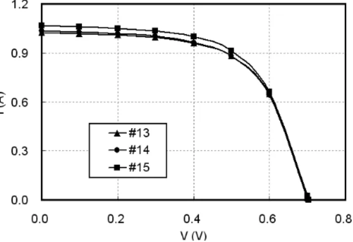
The I-V characteristics of DSSCs employing four TiO2 layers and one scattering layer under simulated AM1.5 irradiation appeared to be nonlinear, as shown in Figure 6. Under short-circuit and scattering layer conditions, the short-circuit current (Isc) increased slightly as the reflection and antireflection films were fabricated. These two factors increased the value of Isc by up to 2.1% as the antireflection film was added. The value of Isc increased by up to 2.5% as the antireflection film was fabricated. The values of Isc were 1.024, 1.035, and 1.068 A. The results were the same in Group 4. However, the values of Isc in Group 5 were higher than those in Group 4, where the average increase ratio was 2.26%. Screen printing one more TiO2 layer can increase Isc by approximately 2.26%.
Figure 6. I-V characteristics for DSSC’s employing four TiO2 layers and one scattering layer
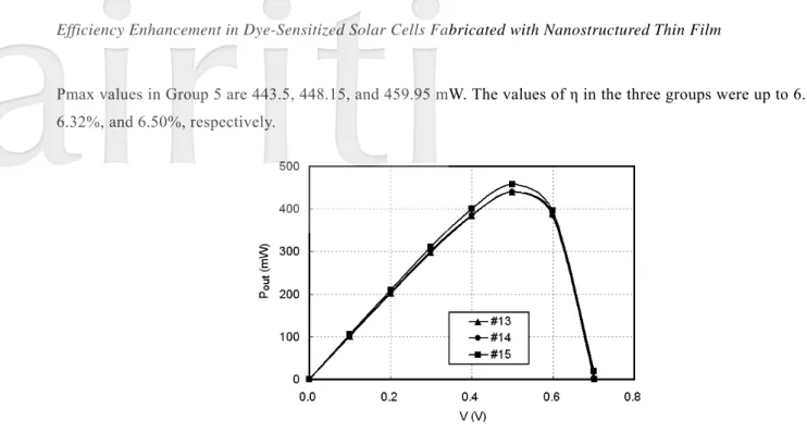
Finally, as shown in Figure 7, the output power Pout appeared to linearly and progressively increase as the DSSC voltage increases. The Pout value reached maximum at approximately 0.5 V. The maximal output power
Pmax values in Group 5 are 443.5, 448.15, and 459.95 mW. The values of η in the three groups were up to 6.25%, 6.32%, and 6.50%, respectively.
Figure 7. Pout-V curves for DSSC’s employing four TiO2 layers and one scattering layer
4. Conclusions
Dye-sensitized solar cells up to 70.92 cm2 in size were tested in our experiment. The thickness of TiO2 film was increased, and antireflection film, reflection film, and scattering layer were fabricated to estimate the DSSC performance. Increasing the thickness of TiO2 linearly increased the photoelectric conversion efficiency (η) of DSSC. The thickness of TiO2 film (in μm) increased η by approximately 0.122%. Fabricating the antireflection film increased the η of DSSC by approximately 0.1%. Fabricating the reflection film increased η up to 0.35%. Fabricating the scattering layer increased the η of DSSC up to 10.79%–1.1%. Based on the above experimental results, fabricating a scattering layer strengthens the performance of DSSCs. The four factors mentioned above can increase the η of DSSC. After fabricating four factors simultaneously, the maximum value of η can be improved by up to 6.5%.
Acknowledgement
This work was financed by the Bureau of Energy, Ministry of Economic Affairs, supporting the DSSC technology development for the industry (Grant No. 9455DI2110).
Reference
[1] Grätzel, M. and O'Regan, B., “A low-cost, high-efficiency solar cell based on dye-sensitized colloidal TiO2 films,” Nature,
Vol. 353, No. 24, pp.737-740, 1991.
[2] Grätzel, M., “Conversion of sunlight to electric power by nanocrystalline dye-sensitized solar cells,” Journal of Photochemistry and Photobiology A: Chemistry, Vol. 164, No. 1-3, pp. 3-14, 2004.
[3] Nazeeruddin, M. K., Angelis, F. D., Fantacci, S., Selloni, A., Viscardi, G., Liska, P., Ito, S., Takeru, B., and Grätzel, M., “Combined experimental and DFT-TDDFT computational study of photoelectrochemical cell ruthenium sensitizers,” Journal of the American Chemical Society, Vol. 127, pp. 16835-16847, 2005.
[4] Chiba, Y., Islam, A., Komiya, R., Koide, N. and Han, L., “Conversion efficiency of 10.8% by a dye-sensitized solar cell using a TiO2 electrode with high haze,” Applied Physics Letters, Vol. 88, No. 22, 223505, 2006.
[5] Chen, Y. S., Lee, J. N., Tsai, S.Y. and Ting, C. C., “Manufacture of dye-sensitized nano cells and their I-V curve measurements,” Materials Science Forum, Vol. 594, pp.324-330, 2008.
[6] Grätzel, M., “Review: dye-sensitized solar cells,” Journal of Photochemistry and Photobiology C: Photochemistry Review, Vol. 4, pp. 145-153, 2003.
[7] Weeks, C., Glatkowski, P. and Britz, D., “Green carbon nanotubes,” Micro Nano, Vol. 12, No. 1, pp. 1-6, 2007.
Research, Vol. 33, pp.27-36, 2000.
[9] Bard, A. J. and Fox, M. A., “Photo-oxidation of water sensitized by TiO2,” Chemical Research, Vol. 28, pp.141-145,
1995.
[10] Yamaguchi, T., Tobe, N., Matsumoto, D., Nagai, T., and Arakawa, H., “Highly efficient plastic-substrate dye-sensitized solar cells with validated conversion efficiency of 7.6%,” Solar Energy Materials & Solar Cells, Vol. 94, pp. 812-816, 2010.
[11] Kroon, J. M., Bakker, N. J., Smit, H. J. P., Liska, P., Thampi, K. R., Wang, P., Zakeeruddin, S. M., Grätzel, M., Hinsch, A., Hore, S., Würfel, U., Sastrawan, R. , Durrant, J. R., Palomares, E., Pettersson, H., Gruszecki, T., Walter, J., Skupien, K. and Tulloch, G. E., “Nanocrystalline dye-sensitized solar cells having maximum performance,” Progress in Photovoltaics: Research and Applications, Vol. 15, No. 1, pp. 1-18, 2007.
[12] Chang, C. W., Chang, C. H. , Lu, H. P., Wu, T. K. and Diau, E. W. G., “Fabrication and photovoltaic characterization of bio- sensitized solar cells using myoglobin-based sensitizers,” Journal of Nanoscience and Nanotechnology, Vol. 8, pp. 1-8, 2008.
[13] Yamaguchi, T., Tobe, N., Matsumoto, D. and Arakawa, H., “Highly efficient plastic substrate dye-sensitized solar cells using a compression method for preparation of TiO2 photoelectrodes,” Chemical Communications, pp. 4767-4769, 2007.