矽化鈷在含鍺介電質形成奈米點並構成非揮發性記憶體之研究
134
0
0
全文
(2) 矽化鈷在含鍺介電質形成奈米點並構成非揮發 性記憶體之研究 Study on CoSi2 nanocrystals in Ge-doped dielectric layer for nonvolatile memory Student:Cheng-Kai Lee (Cheng-En Lee) Advisor:Dr. Bi-shiou Chiou. 國 立 交 通 大 學 電子工程學系 電子研究所 碩 士 論 文 A Thesis Submitted to Department of Electronics Engineering & Institute of Electronics, College of Electrical and Computer Engineering National Chiao Tung University. 中華民國 九十七 年 五 月.
(3) Study on CoSi2 nanocrystals in Ge-doped dielectric layer for nonvolatile memory Student:Sheng-Kai Lee(Cheng-En Lee) --------------Advisor: Dr. Bi-Shiou Chiou. ------------. Department of Electronics Engineering & Institute of Electronics, College of Electrical and Computer Engineering National Chiao-Tung University. ABSTRACT In recent years, digital life has attracted great importance for Taiwan , s electronics market. Then he portable electronic products have been applied widely, such as digital cameras, notebooks, hand-carry USB memories, a chip on credit card , PDA, GPS, memory card, MP3 audio players and so on. However, these portable electronic products are based on the nonvolatile memory (NVM) due to the need of low working power and portability. In a conventional nonvolatile memory (NVM), charge is stored in a ploy-silicon floating-gate (FG). However, it suffers some limitations for continual scaling down of the device structure. In FG memory, the electrons which injected from channel to the poly-silicon trapping layer influence the I.
(4) shift of threshold voltage in the memory. Then it can be defined through the difference of threshold voltages as logic “0” & “1”. Nevertheless, the definition fails if the tunneling oxide provides a leakage path after repeatedly performing write/erase cycling. On other hand, the oxide will produce some defect after repeat impact during electrons the write/erase cycle because the whole structure of FG is semiconductor. All of the charge stored in FG will be trapped into trapping layer or be lost from trapping layer with leak path which was formed with defects. FG structure will have reliability problem when device scale down to nano-meter level. Among the Metal Silicide, cobalt-silicide (CoSi2) has been widely used as a contact source due to the lowest resistivity value ( 10-20 ~μΩcm) and good thermal stability. In this thesis, CoSi2 films were sputtered and we choose rapid thermal annealing (RTA) and sputter system in order to reduce process cost because of temperature controlling and reduce thermal budget because of diffusion reducing. Co-sputtering approach was used to deposit the mixed cobalt, silicon and germanium film. After rapid temperature oxidation (RTO), Novel cobalt silicide nanocrystals embedded in the dielectrics which are doped with Ge have been formed. The charge storage effect of this novel trapping layer have also been investigated by capacitance-voltage (C-V), current density-voltage (J-V) measurement. Transmission Electron Microscopy (TEM), Secondary Ion Mass Spectrometer (SIMS) and X-ray photoelectron spectroscopy (XPS) have been used to analyze formation of the cobalt-silicide nanocrystals. In addition, the structure formed by co-sputtering the Co target with SiO2, Si3N4 target and Al2O3 target have also been demonstrated in this work. The approach also shows good charge storage ability. The charge storage mechanism of various dielectrics has also been revealed by related material analysis.. II.
(5) 矽化鈷在含鍺介電質形成奈米點並構成非揮發 性記憶體之研究. 研究生:李勝凱(李承恩). 指導教授: 邱碧秀 博士. 指導教. 國立交通大學 電子工程學系. 電子研究所. 摘要 近年來,數位生活在台灣電子工業市場扮演了舉足輕重的角色,數位電子產 品的應用已經受到廣大的青睞,像是數位相機、筆記型攜帶式、攜帶隨身聽 MP3 或 CD、信用卡晶片,攜帶型 USB 記憶體或記憶卡和日常生活會用到的 PDA、GPS 等 等。這些個人式電子產品的發展則基於非揮發性記憶體元件的低功率消耗和可攜 式。傳統的非揮發性記憶體是利用複晶矽浮停閘(floating gate)作為載子儲存 的單元,而在元件尺寸持續微縮下,該結構將面臨一些瓶頸。當電子從通道注入 III.
(6) 浮停閘儲存層,記憶體元件將會受到儲存載子影響它本身存在電場的影響,造成 起始電壓的漂移。我們可將受浮停閘改變的起始電壓定義為 1 與 O。然而,因為 這種浮停閘結構為整層的半導體薄膜,在電子反覆的從穿遂氧化層進出這層浮停 閘,會使得穿遂氧化層劣化以至於出現缺陷,當缺陷一旦產生之後,所有儲存的 電子將會隨這層缺陷而產生局部漏電路徑,導致所寫入的儲存載子全部流失掉, 無法達到原本應有之記憶的效果。 矽化鈷是一種金屬矽化合物現今已經因為它本身的低電阻( 10-20 ~μΩcm) 和熱穩定性而被廣大的應用在接觸面上。在本論文中我們使用共同濺鍍和快速退 火系統分別進行薄膜沉積和進行退火。我們會使用快速退火系統是因為溫度控制 的方便性和利用減少熱預算來降低擴散程度。 在本篇論文,我們透過濺鍍系統共打的方式沉積鈷、矽、鍺的混合性薄膜, 再利用快速退火的方式製作一種新穎之矽化鈷物奈米點於含鍺介電層,並研究該 結構金氧絕氧半(MOIOS)結構之儲存效益。除了此金氧半電容結構之C-V、J-V量 測外,並透過一些材料分析如二次離子能譜(SIMS)、X光光電子能譜儀(XPS)釐清 各元素扮演儲存機制之角色。此外,我們亦研究透過共同濺鍍金屬鈷和介電質材 料如氧化矽,氮化矽及氧化鋁作為儲存層,透過電性量測,該結構亦展示不錯之 載子儲存效果,除電性量測外亦透過相關之材料分析X光光電子能譜儀(XPS) 探 討在不同介電質材料之間的形成機制。. IV.
(7) 致. 謝. 這是一個過程,在撰寫本篇論文,在此論文即將完成的同時,研究所的生涯 也即將告一段落。回想起這三年日子的每一天,聽著一些激勵歌曲,酸甜苦澀一 點一滴不由自主的從心中竄起。在此過程,無論是碰到的人、經過的事,真的感 觸良多。要感謝的人相當多,從醫界、學界、業界各式各樣的人都有,感激之情 真的一言難示千意。 首先,要感謝我的指導教授。邱碧秀 博士、 張鼎張 博士及碩一的老師 羅正 U. U. U. U. 忠 博士;三位老師都分別提供我研究方面的指導、讓學生無憂無慮在研究所生涯 U. 致力於學術研究。在研究所的生涯中無論是遇到實驗的瓶頸或是在學業、學務的 關頭。有這三位老師的指導和幫助,真的是相當幸運。最後感謝三位老師在論文 上的指教及建議,讓我的論文能夠更加完善,由衷感謝你們。 在新竹的日子要感謝的人真的太多。感謝 劉柏村 老師在實驗研究上給予的指 U. U. 導及建議,感謝 峻豪 學長、 世青 學長、 立偉 學長、 緯仁 、 志瑋 、 俐婷 、 仕承 、 U. U. U. U. U. U. U. U. U. U. U. U. U. U. U. 睿龍 、 彥廷 、 志晟 、 秀娟 、 宛芳 、 亞諭 等諸多學業夥伴們總是不厭其煩的提供 U. U. U. U. U. U. U. U. U. U. U. 意見及指教,是讓我能在實驗遇到瓶頸時找到解決的出口。特別感謝 邱碧秀 老 U. U. 師, 峻豪 學長、 志瑋 在實驗及論文上的指導及幫忙,不厭其煩的解決我許多實 U. U. U. U. 驗的疑問及提供我更好的建議,今天才能完成這一份充實的論文,著實受益良多。 然而,碩二因為意外分別在 新竹 、 台北 的醫院,但是也得到醫院醫生、護 U. U. U. U. 士、護理師、治療師的鼓勵,他(她)們在忙碌工作之餘,也會鼓勵我。在此一年 特別感謝他(她)們,所以也特別將他(她)們寫在下面,有此論文的完成,他(她) 們在心理的功勞是無法言喻的。同時,他(她)們也建立我想幫助SCI病患的心願。 新竹 馬偕: 郭岱宗 醫師. U. U. U. U. 台北 榮總: 蔡昀岸 、 陳正豐 、 黃敏雄 醫師. U. U. U. U. U. U. U. 雅芳 、 奕如 、 世昌 、 元良 、 儷如. U. U. U. U. U. U. U. U. U. OT、PT治療師. U. 淑賢、雅芳、淑惠、淑偵、淑娟、淑雲、瑞文、慈蓮、欣怡. U. U. U. U. U. U. U. U. V. U. U. U. U. U. U. U. U. 護.
(8) 士、護理師 碩三、我再度回到熟析的 新竹,感謝崔秉鉞老師實驗的 振欽、振銘、曉萱 、 U. U. U. U. U. 雨蓁及一些學弟妹們的幫忙,使我機台複習與實驗的規劃才能夠順利進行,也讓. U. 研究所的日子能夠在這個像大家庭的環境裡生活。吳耀銓老師則鼓勵我。受到大 家許多的照顧。同學、學長、學弟妹們, 貴宇 、 成能 、 培堃 、 聖杰 、 述潁 、 凱 U. U. U. U. U. U. U. U. U. U. U. 庭 、 派璿 、 佑書 、 杼樺 、 孟漢 、 春瑀、嘉政學長、岱瑩也帶給我週遭更多的歡 U. U. U. U. U. U. U. U. U U. U. 樂時光,讓我的研究所生活增加許多的溫暖,這一切都將銘記在心。也感謝中山 大學物理所的 書瑋 學長、 崎峰 學長、 敏甄 ,中央大學材料所的 勝偉 、 宏台 及清 U. U. U. U. U. U. U. U. U. U. 華大學材料所的 偉鑫 學長、炳宏學長等等 在實驗上的幫助。讓我實驗得以順利 U. U. 進行。 AIESEC是我在學生時代最後一個團體,感謝白毛、雨瑄、穎瑄、小敏、兔子、齒 輪,crystal、凱婷、羅傑、靜雅、瀟灑、幹兄…………還有台大的屁屁,很多 人,無法一一列舉。你們真的讓我在這最後的學生時光多了一份視野,也多了一 些友情。AIESEC should be best。 感謝我最親愛的父母及家人,你們的支持與鼓勵是我在研究的路上前進的動 力,因為有你們的愛讓我在挫折時還能勇敢前行,在疲累時給我依靠的溫暖及繼 續堅持在研究的路上走下去的能量,有你們的支持才能讓我無後顧之憂的完成碩 士班學業;最後的最後,謹以此論文獻給你們。. VI.
(9) Contents English Abstract................................................................................……...……………….. I. Chinese Abstract..................................................................................... ………...…........... III. Acknowledgement................................................................................................................... V. Contents.................................................................................................................................. VII Figure Captions...................................................................................................................... Chapter 1 1.1. XI. Introduction. General Background………………………………………………...…………….... 1. 1.1.1. The era of memory…………………………………...…...…………….. 1. 1.1.2. The basic structure of memory……………………………...…………. 5. 1.2. SONOS Nonvolatile memory Devices…………………………………...…...……. 8. 1.3. Nanocrystal Nonvolatile Memory Devices……………………………………..….. 10. 1.4. Motivation…………………………………………………………............................ 14. 1.4.1. Study on formation of cobalt-silicide (CoSi2) nanocrystals for the. application on nonvolatile memory………………………………………............ 16 1.4.2. Post-oxidation annealing procedures of Co-Si-Ge thin film as trapping. layers in oxygen ambient by annealing system………………………………….. 1.4.3. 17. The role of capped oxide during the formation of cobalt-silicide. (CoSi2) nanocrystals in Ge-doped dielectric layer………………………………. 17. Chapter 2 Nonvolatile Memory-basic concept and operation mechanism 2.1. Reading operation……………………………………………………....................... 19. 2.2. Basic Program/Erase Mechanisms…………………………………….…………... 21. 2.2.1. Carrier Injection Mechanisms………………………………….……….. 21. 2.2.2. Channel Hot Electron (CHE) Injection…………...……………….……. 23. VII.
(10) 2.3. 2.2.3. Fowler–Nordheim (FN) Tunneling……………………………….…….. 24. 2.2.4. Direct Tunneling (DT)…………………………………….…………. 26. Basic Physics Characteristics of Nanocrystal Memory………………………….. 2.3.1. Quantum Confinement Effect…………………………………….…….. 26. 2.3.2. Coulomb Blockade Effect……………………………………….…….... 27. Chapter 3 3.1. Experimental procedures. Sample Preparation…………………………………………………….................... Method of Wafer pre-cleaning and fabricating tunnel oxide………… 29. 3.1.2. Method and condition of fabricating Co-Si-Ge thin film……………. 29 Sample study on formation of Cobalt-Silicide (CoSi2). nanocrystals…………………………………………………………....... 3.1.2.2. 3.1.3. 29. Sample study on Post-oxidation annealing procedures of. Co-Si-Ge thin film……………………………………………………….. 30. 3.1.2.3. 31. Sample study on the role of capped oxide………………….. Method and condition of fabricating Co-Si-Ge thin film……………. 32. Physical Characterization Techniques…………………………………………. 3.2.1. Focused Ion Beam (FIB)…………………………………………..……... 3.2.2. Transmission Electron Microscopy (TEM) and Energy dispersive X-ray spectroscopy (EDX)…………………………………………………….... 3.3. 29. 3.1.1. 3.1.2.1. 3.2. 26. 36 36. 36. 3.2.3. X-ray photoelectron spectroscopy (XPS)………………………………... 36. 3.2.4. secondary ion mass spectrometry (SIMS)……………………………….. 36. Physical Characterization Techniques………………………………………….. Chapter 4. Results and Discussion VIII. 37.
(11) 4.1. Study on formation of cobalt-silicide (CoSi2) nanocrystals for the application on. nonvolatile memory……………………………...……..………………… 4.2. 38. Post-oxidation annealing procedures of Co-Si-Ge thin film as trapping layers in 43. oxygen ambient by annealing system………………………………………….... 4.2.1. Results…………………………………………………… 45. 4.2.1.1. Electrical characteristics………………………………………... 45. 4.2.1.2 4.2.2. 4.3. Material analysis…………………………………….. The discussion…………………………………………… 56. 4.2.2.1. Discussion on electrical characteristics……………... 56. 4.2.2.2. Reaction free energy………………………………… 57. 4.2.2.3. Formation of CoSi2 nanocrystal after annealing……. 58. The role of capped oxide during the formation of cobalt-silicide (CoSi2). nanocrystals in Ge-doped dielectric layer……………………………………………….... Chapter 5 5.1. 46. 62. Conclusion. Conclusion………...…………………………………………………................... 71. Addendum A Metal Co-SiO2 and Co-Si3N4 co-sputtering as trapping film of Cobalt mixtures and future development A.1. Motivation…………………………………………………....................................... 73. A.2. Experimental procedure………………………………………………………….... 74. A.3. Results and discuss…………………………………………………………………. 76. A.4. Summary and future development………………..………………………………. 89. A.5. Future development………………………………………………………………... 89. Addendum B Observations of metal Co-Al2O3 co- sputtering and future development IX.
(12) B.1. Motivation………………………………………………………………................... 91. B.2. Experimental procedure………………………………………………………….... 91. B.3. Results and Discussion……………..………………………………………………. 93. B.4. Summary………………………………………..…..………………………………. 101. B.5. Future development………………………………………………………………... 102. References Chapter 1...........................................................................……...…………………………... 104. Chapter 2............................................................................……...…………………………. 109. Chapter 4................................................................................................................................. 111. Addendum A.......................................................................................................................... 113. Addendum B.......................................................................................................................... 114. X.
(13) Figure Captions Chapter 1 Figure 1-1 The structure of the conventional floating gate nonvolatile memory device. Continuous poly-Si floating gate is used as the charge storage element. (Ref. Simon M. Sze, Kwok K. Ng, s "Physics of Semiconductor Device". Wiley, New. York..................................................................................................................................... 2 Figure 1-2 The history of memory tree………………………………………………………………. 4. Figure 1-3 History of NVM (SONOS structure) (Ref. Toshiba Corporation ULSI Research Center “Technology Trend of FlashEEPROM — Can Flash-EEPROM overcome DRAM?”, Symposium on VLSI Technology Digest of Technical Papers, 1992, pp.6~9.)………………………………… 6 Figure 1-4 Basic structure of FAMOS (Ref. Frohman-Bentchkowsky, D. “A fully decoded 2048-bit electrically programmable FAMOS read-only memory “ Solid-State Circuits, IEEE Journal of, Volume: 6,. Issue:. 5 1971…………………………………………………………………………………….. 7. Figure 1-5 (A) basic structure of SAMOS (B) basic structure of SIMOS (Ref. “Technology of a new n-channel one-transistor EAROM cell called SIMOS Electron Devices” IEEE Transactions on 1977)…………………………………………. 7 Figure 1-6 SONOS structure memory……………………………………………………………….. 9 Figure 1-7 MNOS structure memory. 1960s~1970s………………………………………………. 10. Figure 1-8 The energy band diagrams of the write/erase operation for a SONOS device………….... 11. Figure 1-9 The structure of the nanocrystal nonvolatile memory device. The semiconductor nanocrystals or metal nanodots are used as the charge storage element instead of the continuous poly-Si floating gate………………………………………………………..... 13. Chapter 2 Figure 2-1. Floating-gate MOSFET reading operation. XI.
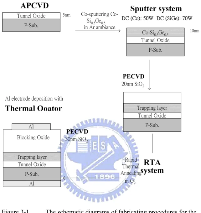
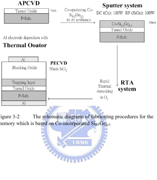
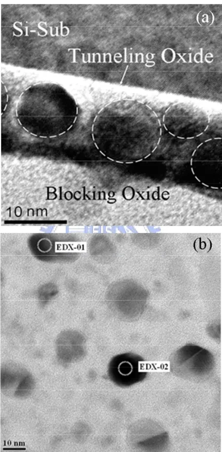
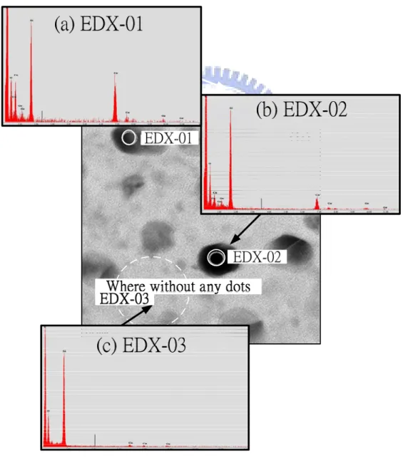
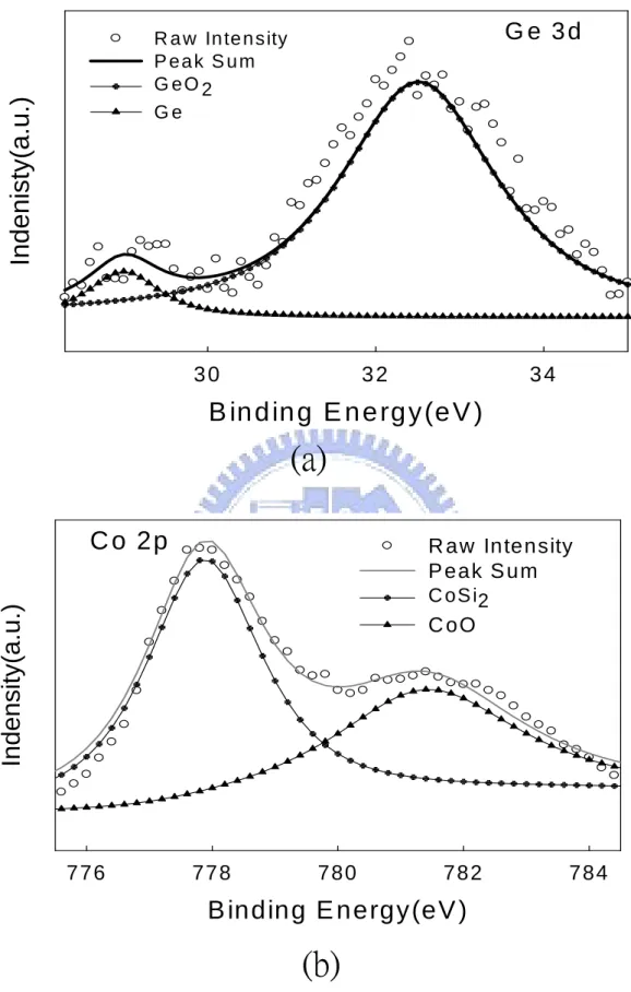
(14) ( Ref. Roberto Bez,Emilio Camerlenghi,Alberto Modelli,Angelo Visconti., Introduction to Flash Memory, proceedings of the IEEE, VOL. 91, NO. 4, APRIL 2003)……………………………………………………………………………………... 20 Figure 2-2. Memory band diagram in (a)write mode. (b)Erase mode………………………………. Figure 2-3. Fourth approaches to programming methods, described by Hu and White. 22. ( Ref. Amit K. Banerjee, Yin Hu, Matthew G. Martin and Marvin H. White, An Automated SONOS NVSM Dynamic Characterization System, 0-7803-1290-N3 $3.00 01993 IEEE) …………………………………………………………………………….. 23 Figure 2-4. Coulomb blockade effect……………………………………………………………….... 28. Chapter 3 Figure 3-1. The schematic diagrams of fabricating procedures for the memory which is based on Co-incorporated Si0.5Ge0.5……………………………………………………………………………………………….... Figure 3-2. The schematic diagrams of fabricating procedures for the memory which is based on Co-incorporated Si 0.5Ge0.5………………………………………………………………………………………………... Figure 3-3. 33. 34. The schematic diagrams of fabricating procedures for the memory which is based on CoSi2-incorporated Si0.5Ge0.5……………………………………………………………………………………………. 35. Chapter 4 Figure 4-1. The C-V characteristics of the Co- Si-Ge co-sputtered film with capped oxide before annealing. ……………………………………………………………………………………………….......................................... Figure 4-2. The J-V characteristics of the Co- Si-Ge co-sputtered film with capped oxide before annealing. ……………………………………………………………………………………………….......................................... Figure 4-3. 39. 40. (a) the cross-sectional and (b) the plane-view TEM image of the fabricated device sample. ………………………………………………………………………………………………................................................ 41. Figure 4-4. The EDX images of the fabricated device sample after RTO process…………………… 42. Figure 4-5. The XPS spectrum of (a) Ge 3d and (b) Co 2p3/2 in the Co-Si0.5Ge0.5 co-sputtered. XII.
(15) film after thermal oxidation process…………………………………………………….... 44. Figure 4-6. Figure 4-6 C-V hysteresis of the fabricated device sample after RTO process…………... 46. Figure 4-7. The cross-sectional TEM and the C-V hysteresis of the fabricated device sample after lower temperature RTO process………………………………………………………….. Figure 4-8. 47. (a) Cross-sectional TEM and EDX (Energy Dispersive X-ray analysis) of the fabricated device sample after RTO process. (b) The quantitative analysis and could understand that oxygen elements on the point…………………………………………… 49. Figure 4-9. The XPS spectrum of (a) Ge 3d and (b) Co 2p3/2 in the Co-Si0.5Ge0.5 co-sputtered film after thermal oxidation process…………………………………………………….... Figure 4-10. 51. The cross-sectional TEM and the C-V hysteresis of the fabricated device sample after higher temperature RTO process……………………………………………………………………………………. 52. Figure 4-11. Cross-sectional TEM and EDX (Energy Dispersive X-ray analysis) of the fabricated device sample after RTO process………………………………………………………… 53. Figure 4-12. The XPS spectrum of (a) Ge 3d and (b) Co 2p3/2 in the Co-Si0.5Ge0.5 co-sputtered film after thermal oxidation process in higher temperature……………………………… 54. Figure 4-13. The J-V characteristics of the capacitor based on the Co- Si0.5Ge0.5 co-sputtered film with oxidation in different condition……………………………………………………... Figure 4-14. 56. (a) he C-V hysteresis of the fabricated device sample and (b) the quantity of trapped charge after RTO process………………………………………………………………… 57. Figure 4-15. The oxidation and aggregative mechanism in the Co- Si0.5Ge0.5 co-sputtered thin film without capped oxide……………………………………………………………………... Figure 4-16. The C-V characteristics of the Co-Si-Ge co-sputtered film with CoSi2 and SiGe targets (a) with and (b) without capped oxide before annealing. ………………………………. Figure 4-17. 61. The structure (a) with and (b) without capped oxide can be appear on the. XIII. 63.
(16) Figure 4-18 Figure 4-19 Figure 4-20. Cross-sectional TEM. ……………………………………………………………………. 65. The results of SIMS analysis for the cobalt silicon germanium mixed film (a) with\ (b) without capped oxide. ……………………………………………………………………. 67. The J-V characteristics of the capacitor based on the Co- Si-Ge co-sputtered film with oxidation in different condition. …………………………………………………………. 68. Data (a) endurance and (b) retention characteristics of the memories which are based on cobalt-silicide nanocrystals. …………………………………………………………. …. 70. Addendum A Figure A-1. The process flow of structure is (a) SiO2/Co-SiO2/ SiO2/Si and (b) Si3N4/Co- Si3N4/ SiO2/Si in this work. . …………………………………………………………..…...… 75. Figure A-2. Transmission electron microscopy (TEM) analyses and its EDX. After annealing cobalt elements had accumulated to form cobalt nanocrystals which were embedded between tunnel oxide and control oxide after anneal at 750℃ and during 30 seconds.. 77. Figure A-3. The C-V hysteresis of the memory which is based on Co-SiO2 co-sputtered file……... 78. Figure A-4. The C-V hysteresis of the memory which is based on Co-Si3N4 co-sputtered file…….. Figure A-5. The relations between gate voltage and flat-band voltage, stored charges in a MIS. 79. capacitor. The insets in this figure the high frequency C-V relations of MIS capacitors co-sputtered to form the charge storage film with metal Co embedded in the Si3N4 during different annealed time respectively…………………………………………… Figure A-6. The XPS spectra of Co 2p3/2 peaks in the memory which is based on Co-SiO2 co-sputtered film……………………………………………………………………. Figure A-7. 81. 83. The XPS spectra of Co 2p3/2 peaks in the memory which is based on Co-Si3N4 co-sputtered film……………………………………………………………………….. 84. Figure A-8. (a) the SIMS analysis of Co-SiO2 co-sputtered film which was annealed during 60 sec in different temperature ambiance (b) the SIMS analysis of Co-Si3O4 co-sputtered film which was annealed during 60 sec in different temperature ambiance………….. 86. Figure A-9. The J-V characteristics of the memory which is based (a) on the Co-SiO2. XIV.
(17) co-sputtered film (b) on the Co-Si3N4 co-sputtered film………………………………. 87 Figure A-10. The endurance characteristics of the MOIOS with Co nanocrystals embedded in the (a) Co-SiO2 and (b) Co- Si3N4 co-sputtered film………………………………………. Figure A-11. 88. The charge retention characteristic of memory which was based on Co-SiO2 co-sputtered film……………………………………………………………………….. 88. Addendum B Figure B-1. The process flow of the structure with Al2O3-Co co-sputtered film………………….... Figure B-2. The C-V characteristics of Al/SiO2/ “The charge storage layer”/ SiO2/Si-based as MIS structure, showing hysteresis of as-deposited and after PTA at 650 ◦C and 750 ◦C measured. The curves were obtained by gate voltage sweeping from forward to reverse and back……………………………………………………………………….. 94. Figure B-3. The illustrative band diagram of a MIS structure (Al/SiO2/ “The charge storage layer”/ SiO2/Si) with positive applied voltage at metal gate………………………….... Figure B-4. 92. 94. The C-V characteristics of Al/SiO2/ “The charge storage layer”/ SiO2/Si-based as MIS structure, showing hysteresis of as-deposited and after PTA at 650 ◦C and 750 ◦C measured during different time. The curves were obtained by gate voltage sweeping from forward to reverse and back…………………………………………………….... Figure B-5. 96. The relations between gate voltage and flatband voltage, stored charges in a MIS capacitor. The insets in this figure the high frequency C-V relations of MIS capacitors co-sputtered to form the charge storage film with metal Co embedded in the Al2O3 and Si3N4 respectively………………………………………………………………….. Figure B-6. 97. The XPS (ESCA) spectra of Co-O and Al-O peaks in Co-Al2O3 co-sputtered film after RTA annealing in N2 ambiance. We could know that is CoxOy-AlzOw mixture clearly…………………………………………………………………………………... 98. Figure B-7. The TEM image of Co-Al2O3 co-sputtered film and its EDX…………………………. 100. Figure B-8. I-V characteristics of the memory which is based on Co-Al2O3 co-sputtered film with. XV.
(18) 750oC annealing process during 60 seconds………………………………………….... 101. Figure B-9. The endurance of the memory which is based on Co-Al2O3 co-sputtered film………... 101. Figure B-10. (a) the discontinuous grain memory with material (Corich- (CoxAl1−x) zO3−v) and (b) the SONOS structure memory with material (CoxAl1−x) zO3−v…………………………………….... XVI. 103.
(19) Chapter 1 Introduction To begin our study of memory, we need to address two central issues. First, what is memory? Second, what is the goal of research on memory?. 1.1 General Background 1.1.1. The era of memory. In recent year, the portable electronic product have widely been applied due to the concept of low cost、small volume and power-saving develop. Because of them, digital life has attracted great importance for electronics market in Taiwan. Then the portable electronic products have been applied widely, such as digital camera, notebook computer, MP3 walkman, hand-carry USB memory, a chip on credit card , PDA, GPS, memory card, MP3 audio players and so on. However, the electronic industry was subjected that electronic market was challenging it. The electronic industry urgently needs a new memory device to replace the magnetic-core memory because of its power consumption or other drawbacks then. Therefore, D. Kahng and S. M. Sze invented the floating-gate (FG) nonvolatile semiconductor memory (or flash memory) at Bell Labs in 1967 [1.1] [1.2]. The stacked-gate FG device structure is shown in Fig. 1-1. Although a huge commercial success, conventional FG devices have their limitations. The trapped charges in the floating gate can be thermally stable without the disturbance by electric field and high temperature. However .it has a poly-silicon gate completely surrounded by dielectric.. 1.
(20) Control Gate Blocking oxide or Control oxide (ONO stack) Floating Gate(poly-silicon) Tunnel oxide. Source. Drain Si-substrate. Figure 1-1 The structure of the conventional floating gate nonvolatile memory device. Continuous poly-Si floating gate is used as the charge storage element. (Ref. Simon M. Sze, Kwok K. Ng, s "Physics of Semiconductor Device" Wiley, New York. Because of their research on memory and FG was invent, the electronics industry and market rapidly develop in Taiwan and world. We believe no one can diminish or deny the victory memory device has scored. The rapidly developed Endure rice science and technology allows us to explore more of it secret. The present storing device can be split into two main categories: One kind is volatile memory such as SRAM or DRAM and another is nonvolatile memory such as ROM、EPROM (Erasable Programmable Read Only Memory)、EEPROM (Erasable Programmable Read Only Memory). The volatile memory loses any data they store when the power is turned off; it requires constant power to remain viable. Most types of random 2.
(21) access memory (RAM) are very dense and have fast speed in writing and reading. RAM is massive applied in computer industry. The nonvolatile memories, we also could call NVM device, are a basic MOS transistor that has a source, a drain, an access, a control gate and a floating gate. It is structurally different from a standard MOSFET in its floating gate, which is electrically isolated, or "floating". The nonvolatile memories are subdivided into two main classes: floating gate and charge-trapping. The nonvolatile memory does not lose its data when the system or device is turned off (power off) named ROM, opposite one data will be lost or said volatile after power off named RAM. It was showed in Fig. 1-2. These two kinds of memories are most different in their data retention. In this research, research on nonvolatile memory is our priority. Although a huge commercial success, conventional FG devices still come to be in face of and challenge their limitations. The most prominent one is the limited potential for continued scaling down of vertical stack structure. This scaling limitation stems from the extreme requirements put on the tunnel oxide layer. Since the SiO2 barrier between the floating gate and the MOSFET channel is thinner, its quality is critical to ensure good floating gate isolation. There were three major types of nonvolatile memory: (1) conventional FG memory (2) SONOS memory (3) nanocrystal memory. These memories have quick program/erase speed and low power losing.. 3.
(22) Figure 1-2. The history of memory tree. Moreover, in the coming years, portable systems will demand even more nonvolatile memories, either with high density and very high writing throughput for data storage application or with fast random access for code execution in place. Those digital products are based on the flash memory which is one kind of the nonvolatile memory that can be electrically erased and reprogrammed when power is off, so the flash memory device was more and more import in the world. The flash memory is the most important among the semiconductor industry. It can be classified into two major markets in Taiwan: code storage application and data storage application. In this chapter, we will introduce that some memory device how to develop in Taiwan and world, such as memory composed of metal nanocrystal2. In addition, the flash memory fabrication process is compatible with the current CMOS process and is a suitable solution for embedded memory applications. Therefore, flash memories are easily scalable replacements for EPROM (Erasable Programmable Read Only Memory) and EEPROM (Electrically Erasable Programmable Read Only Memory). EPROM can be electrically programmed, and need to be exposed to the ultra-violet 4.
(23) (UV) radiation for erasing the storage charge. However, EEPROM can be electrically erasable and programmable. Flash memories are new breeds of NVM in which not only every cell can be electrically programmed but also electrically erased at a large scale of cells at the same time. Since flash memory possesses these key advantages, it has become the mainstream nonvolatile memory device nowadays.. 1.1.2. The basic structure of memory. In this kind of memory, electrons were transferred from the floating gate to the substrate by tunneling through about 3~5 nm thin silicon dioxide (SiO2) layer or other high-k dielectric materials [1.3]. Tunneling is the process by which an NVM can be either erased or programmed and is usually dominant in thin oxides of thicknesses less than 12 nm. Storage of the charge on the floating gate allows the threshold voltage (VT) to be electrically altered between a low and a high value to represent logic 0 and 1 respectively. In floating gate memory devices, charge or data is stored in the floating gate and is retained when the power is removed. They consist of a stacked gate MOS transistor. Show like the above, there were three major types of nonvolatile memory: (1) conventional FG memory (2) SONOS memory (3) nanocrystal memory. For the conventional FG memory, Because of several defects such as interface defects in the tunnel oxide, they might induce a leakage path and all charge stored from the FG leaking back to the channel. That is why the conventional FG memory always needs thicker tunnel oxide to get better retention. There are many researches about leakage or high-K material in the world. From them, we can understand that its importance is not out of consideration about its operations. In order to overcome the scaling limitations of the conventional FG memory structure, SONOS memories [1-4 to 1-6] and nanocrystal memories [1-7 to 1-9] are two most mentioned candidates. We also 5.
(24) could clearly understand that the development history of NVM devices in Fig. 1-3 for SONOS memories structure in Intel corporate. One of them was FAMOS (Floating gate Avalanche injection MOS) device. It introduced by Frohman-Bentchkowsky [1-10]. High energetic electron created in the drain avalanche plasma writing the devices. Erasure is possible by UV or X-ray radiation. Fig. 1-4 was FAMOS. It was first operating floating gate device. And then, SAMOS (Stacked gate Avalanche injection MOS) is in Fig. 1-5(A) and was showed in [1-11]. This kind of device is written like FAMOS device. However, several difference in erasure mechanisms between FAMOS and SAMOS. Another, SIMOS cell was the n-channel version of the SAMOS devices Fig. 1-5(B). It was showed in [1-12]. Programming operation occurs because of Channel hot-electron (CHE) injection. This cell was used mainly for EPROM applications.. Figure 1-3. History of NVM (SONOS structure). (Ref. Toshiba Corporation ULSI Research Center “Technology Trend of FlashEEPROM — Can Flash-EEPROM overcome DRAM?”, Symposium on VLSI Technology Digest of Technical Papers, 1992, pp.6~9. ). 6.
(25) Figure 1-4. Basic structure of FAMOS. (Ref. Frohman-Bentchkowsky, D. “A fully decoded 2048-bit electrically programmable FAMOS read-only memory “ Solid-State Circuits, IEEE Journal of, Volume: 6,. Issue: 5 1971. Figure 1-5 (A) basic structure of SAMOS (B) basic structure of SIMOS (Ref. “Technology of a new n-channel one-transistor EAROM cell called SIMOS Electron Devices” IEEE Transactions on 1977) 7.
(26) 1.2 SONOS Nonvolatile memory Devices SONOS is the abbreviation of a basic memory. We could clearly understand that its basis structure is poly-Silicon/ (control or blocking) Oxide/Nitride/ (tunneling) Oxide/Silicon and show it in Fig. 1-6. The first nitride-base memory devices were extensively studied in the early 70s after the first metal-gate nitride device Metal/Nitride/Oxide/Silicon (MNOS) was reported in 1967 by Wegener et al [1-13]. It is showed in Fig. 1-7. However, MNOS were p-channel structures with aluminum gate electrodes and thick (45 nm) silicon nitride charge storage layers. Write/erase voltages were typically 25-30 V. In the late 1970s and early 1980s, scaling moved to n-channel silicon-nitride-oxide-silicon (SNOS) devices with write/erase voltages of 14-18 V. It is showed in. In the late 1980s and early 1990s n- and p-channel SONOS devices emerged with write/erase voltages of 5-12 V. SONOS based nonvolatile memory has emerged as the most mature nonvolatile semiconductor memory (NVSM or NVM) currently in use for a wide range of applications in our daily life and becomes the most popular charge trapping device because of its complete compatibility with existing advanced it CMOS technology. On the other hand, the SONOS memory device has received a lot f attention due to its advantages over the traditional floating-gate flash EEPROM device such as including reducing process complexity, lowering voltage operation, getting higher operation speed, improving cycling endurance and elimination of drain-induced turn-on [1-14]- [1-17]. The basis of this kind memory is trapping charge to change its threshold Voltage. Aside from them, they also can cost down because that it can achieve two-bit per cell. The charges of storage elements in SONOS memory are the charge traps distributed throughout the volume of silicon nitride layer. A typical trap has a density of order 1018~ 1019cm-3 according to Yang et al [1.18] and stores both electrons and holes. 8.
(27) (positive charges) injected with F-N or direct tunneling from the channel. The intrinsic distributed storage is an advantage of the SONOS device over the FG device. It has improved endurance, since a single defect will not cause the discharge of the memory. In the meantime, SONOS memories hardly reach a data retention for 10 years. This is why the actual use of SONOS memories is limited to military applications needing high radiation hardness [1-19] and [1-20].. Figure 1-6. SONOS structure memory. 9.
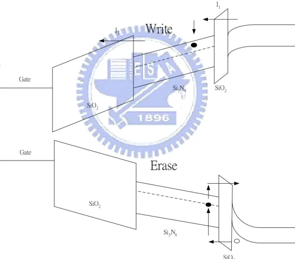
(28) Figure 1-7. MNOS structure memory. 1960s~1970s. 1.3 Nanocrystal Nonvolatile Memory Devices The program/erase mechanism is shown in Fig. 1-8. SONOS devices are programmed by channel hot electron (CHE) injection or Fowler-Nordheim (F-N) tunneling mechanism, mainly. In general, the program speed in CHE injection is 102~103 times faster than in F-N tunneling [1-21]. During programming, the control gate is biased positively so that electrons from the channel can tunnel across the SiO2 into the nitride layer with F-N tunneling mechanism I1 and some electrons will continue to move through the nitride layer then across the control oxide finally into the control gate I2 with the same mechanism. Last, saturation of charging will be reached when I1=I2. The remaining trapped charges in the nitride layer provide the electrostatic screening of the channel from the control gate. Therefore, there is a 10.
(29) threshold voltage shift (ΔVT) resulting from trapped charges in nitride and because of that SONOS can be used as a memory device just like conventional floating gate devices. Last, the SONOS memory device still has to face the challenge in the future for high density nonvolatile application, which require lower power (<5V), lower power consumption, faster operation speed, longer retention time and superior endurance characteristics.. Figure 1-8 The energy band diagrams of the write/erase operation for a SONOS device.. 11.
(30) In the early 1990s nanocrystal nonvolatile memories first was introduced by IBM researchers. Some of the most compelling studies have focused on the flash memory with a granular floating gate made out of silicon nanocrystals [1-22] [1-23]. Fig. 1-9 illustrates nanocrystal nonvolatile memory device structures. The employment of Si nanocrystals as discrete floating gates is a promising way to limit the lateral charge communication in an EEPROM, which in consequence provides a means for extending the scaling limit of flash memories. The tunneling oxide thickness of this memory device was 4.5 nm. Writing/Erasing time was smaller than 100 nanoseconds. Writing/Erasing number of times was greater than 109 times. Operating voltage was 2.5V and long retention time. Those proved that using discontinuing FG replacing continuing FG maybe nice method of improving floating gate memory. On the other hand, charge was not stored on a continuous FG poly-Si layer, but instead on a layer of discrete, mutually isolated, crystalline nanocrystals or dots typically made of semiconductor material. Each dot will typically store only a handful of electrons which tunneled from channel. Collectively the charges stored in these dots control the channel conductivity of the memory transistor. The charges loss often through lateral paths in nanocrystal-based memory devices can be suppressed by the oxide isolation or other insulator such as high-k material between nanocrystals, these devices exhibited superior charge storage characteristics compared with conventional floating-gate memory devices. All stored charges won’t be lost through the few leaky paths since the charges are stored in distributed nanocrystals or called nanodots.. 12.
(31) Figure 1-9 The structure of the nanocrystal nonvolatile memory device. The semiconductor nanocrystals or metal nanodots are used as the charge storage element instead of the continuous poly-Si floating gate. When comparing with conventional stacked gate NVSM devices the charge storage on nanocrystal offers several advantages. The first thing we notice is that its thinner tunnel oxide without sacrificing data volatility. Because of this, reducing the tunnel oxide thickness is not only a key to lowering operating voltages but also increasing operating speeds. This claim of improved scalability results not only from the distributed nature of the charge storage, which makes the storage more robust and fault-tolerant, but also from the beneficial effects of Coulomb blockade [1-24] and quantum confinement effects (band-gap widening; energy quantization). However, both them can be exploited in sufficiently small nanocrystal geometries (about sub-3 nm dot diameter) to further enhance the memory performance. There are some other important advantages. First, nanocrystal memories use a more simplified fabrication process as compared to conventional stacked-gate FG. 13.
(32) NVM by avoiding the fabrication complications and reducing costs of a dual-poly process. Further, due to decrease the effects of Drain -FG coupling, nanocrystal memories suffer less from drain-induced-barrier-lowering (DIBL).because of this, these devices have intrinsically better punch-through characteristics. One way to exploit this advantage is to use a higher drain bias during the read operation, thus improving memory access time. Alternatively, it allows the use of shorter channel lengths and therefore smaller cell area (i.e., lowering cost). Finally, nanocrystal memories are characterized by excellent immunity to stress induced leakage current (SILC) and oxide defects due to the distributed nature of the charge storage in the nanocrystal layer. Unlike volume distributed charge traps (ex: nitride in SONOS NVM or some high-k material [1-25]), nanocrystals be deposited in a two-dimensional layer at a fixed distance from the channel separated by a thin tunnel oxide. By limiting nanocrystals deposition to just one layer and adjusting the thickness of the top blocking dielectric, charge leakages to the control gate from the storage nodes can be effectively prevented. However, there are some intrinsic weaknesses as well. Of particular importance is the low capacitive coupling between the external control gate and the nanocrystal charge storage layer. This does not only result in higher operating voltages, thus offsetting the benefits of the thinner tunnel oxide, but also removes an important design parameter (namely the coupling ratio) typically used to optimize the performance/reliability trade-off.. 1.4 Motivation Because the portable electronic products have been widely applied, we have 14.
(33) known that the memory plays an important role in the market on chapter 1-1 and I won’t restate. In recent years, there are many researches on semiconductor or metal nanocrystals as memory and considerable attention has been focused on semiconductor or metal nanocrystals embedded in the silicon dioxide of a metal oxide semiconductor (MOS) device for future high speed and low power consuming memory device. The self-assembling of silicon or germanium nanocrystals embedded in SiO2 layers has been widely studied, and strong memory effect in MOS devices were reported [1-26]. The major advantages of metal nanocrystals over semiconductor include (1) high density of states around the Fermi level, (2) strong coupling between the nanocrystal and the substrate [1-31] (3) a wide range of available work function, and (4) smaller energy perturbation due to carrier confinement. I had chosen a kind of metal as the storage material of memory device because of those advantages. The metal material I chosen was cobalt. On the other hand, our researches were chosen cobalt or cobalt Silicide as the main materials for some reasons. Among several kinds of nanocrystals devices, the metal and metal-silicide NCs are considered to be beneficial in its variable work function, higher density of states around the Fermi level and so on. We could know that metal silicide has been receiving attention in VLSI devices for interconnects, gate and source/drain contacts. Among the Metal Silicide, cobalt-silicide (CoSi2) has been widely used as a contact source due to the lower resistivity value (10-18μΩ/cm) and good thermal stability [1-32]. Over the past years, several studies have been made on the memory that was based on Co or CoSi2 nanocrystals. CoSi2 thin films are often employed in the semiconductor technology. They have been mentioned that there was a nice method used to form CoSi2 nanocrystals embedded dielectric layer such as SiO2. We observed that the CoSi2 nanocrystals were nucleated in SiO2 layer, leading to an obvious memory effect [1-33]. However, CoSi2 nanocrystals embedded Si0.5Ge0.5 layer has 15.
(34) never been studied so far. There were a lot of experiments forming Ge nanocrystal by oxidizing the Si0.5Ge0.5 film. Germanium (Ge) element is also a semiconductor; SiGe Semiconductor plays a key role in enabling these technologies by providing high-performance, low-cost power amplifiers and chip-scale RF front-end modules that comply with the latest wireless standards and market requirements. The transistor uses a modified design and IBM's proven silicon germanium (SiGe) technology to reach speeds of 210 Gigahertz (GHz) while drawing just a milliamp of electrical current. This represents an 80 percent performance improvement and a 50 percent reduction in power consumption over current designs. Germanium element has higher dielectric constant (~16.0, i.e., stronger coupling with the conduction channel). Germanium element may improve data retention time due to its smaller energy band gap. Because of these, we think that germanium element maybe good memory device fabrication materials. Germanium element component was added into the Si and Co mixed layer. At the same, we tried to deposit Si0.5Ge0.5 thin film by co-sputter system and then anneal it by Rapid Thermal Annealing (RTA) system. We chose RTA to avoid Ge or Co over oxidizing. Several studies have been made on this memory which is based on the Si0.5Ge0.5 co-sputtered film. We also ascertain what role Ge and Co plays on the memory devices. A three-phase study was designed to explore the formation of cobalt-silicide, the role of capped oxide before RTA and the procedure of oxidation mechanism. It this investigation about co-sputtered film we carried out three different experiment procedures and materials.. 1.4.1. Study on formation of cobalt-silicide (CoSi2) nanocrystals. for the application on nonvolatile memory Among several kinds of NCs devices, the metal and metal silicide NCs are 16.
(35) considered to be beneficial in its variable work function, higher density of states around the Fermi level. In addition, the dielectric layer that NCs embedded in also can contribute the charge storage sites by defects or traps created in the interfaces between different materials10-11. In this investigation, the formation of cobalt-silicide NCs was investigated by adding Ge elements into the cobalt-silicide film using co-sputtered Co and Si0.5Ge0.5 targets on tunnel oxide. After thermal oxidation process, the cobalt-silicide NCs are formed and the additional Ge elements are oxidized. Furthermore, the oxidized Ge elements contribute extra charge trap sites.. 1.4.2. Post-oxidation annealing procedures of Co-Si-Ge thin. film as trapping layers in oxygen ambient by annealing system In previous section, we have studied on formation of cobalt-silicide (CoSi2) nanocrystals and the role of capped oxide during the formation of cobalt-silicide (CoSi2) nanocrystals in Ge-doped dielectric layer. We could understand that capped oxide plays a important role. In this section, let us now shift the emphasis away from the sample with cap to the sample without cap and let us examine the mechanism of oxidation in more detail. We chose pure Co and Si0.5Ge0 targets to form a Corich-Si-Ge thin film with sputter system because the SiO2 and GeO2 reaction is thermodynamically more preferable than CoO during annealing. Sufficient Co atoms could react with silicon to CoSi2 nanocrystals according to previous section. It could realize the procedure of oxidation mechanism when the samples are annealed with varies material analysis.. 1.4.3. The role of capped oxide during the formation of. cobalt-silicide (CoSi2) nanocrystals in Ge-doped dielectric layer 17.
(36) The floating-gate memory have faced a challenge to devices scaling down [1-34]-[1-35]. Among the reported literature, a structure with distributed nanocrystals as charge storage sites is considered a potential resolution to replace the conventional memory structure [1-36]-[1-37]. Many different researches of the nanocrystals such as the development of material, the improvement of performance and the electrical operation of nanocrystals devices have been reported in the recent year [1-38] to [1-43]. In the development of material, the structure combined with cobalt-silicide nanocrystals and oxidized germanium is presented as a trapping layer for the application of nonvolatile memory [1-44]. In order to form the cobalt-silicide nanocrystals and oxidized germanium, rapidly thermal oxidation (RTO) is necessary. However, the parameter of RTO process is difficult to control such as the flow rate of oxygen or the time of process affects the aggregation of nanocrystals seriously. In this thesis, the aggregation behavior of cobalt-silicide nanocrystals during the RTO process has been studied. The results of Transmission electron microscopy (TEM) and Secondary Ion Mass Spectrometer (SIMS) indicate that the capped oxide enhances the aggregation of nanocrystals obviously. It also restrains the diffusion and oxidation behaviors of Co and Ge during thermal treatment. Therefore, a capped oxide before RTO process is essential for the aggregation of cobalt-silicide nanocrystals in Ge-doped dielectric layer by RTO process.. 18.
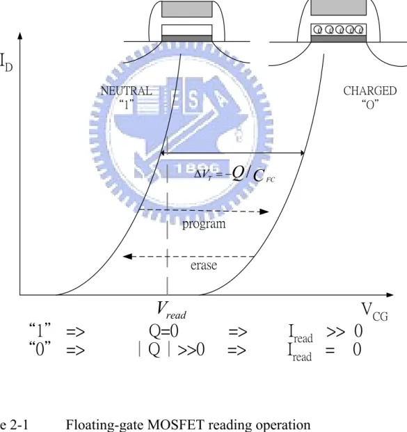
(37) Chapter 2 Nonvolatile Memory basic concept, operation mechanism and material analysis. 2.1 Reading operation In this chapter, the program and erase mechanisms of nonvolatile memory device will be introduced. Most of operations on novel nonvolatile memories, such as nanocrystal and SONOS memories are base on the concept of Flash memory. The data stored in a Flash cell can be determined measuring the threshold voltage of the FG MOS transistor. The best and fastest way to do that is by reading the current driven by the cell at a fixed gate bias. If a dot or nanocrystal has to be stored in a bit of the memory, there will be different procedures. In the current–voltage plane two cells, respectively, logic “1” and “0” exhibit the same transconductance curve but are shifted by a quantity—the threshold voltage shift (ΔVt ). The threshold voltage shift of a flash transistor can be written as. ΔVT = −. Q C. FC. Where Q is the charge weighted with respect to its position in the gate oxide and CFC is the capacitances between the floating gate and control gate. Hence, once a proper charge amount and a corresponding is defined, When writing operation is completed it is possible to fix a reading voltage in such a way that the current of the “1” cell is very high (in the range of tens of microamperes), while the current of the “0” cell is zero, in the microampere scale. It is showed in Fig. 2-1 clearly. In this way, 19.
(38) it is possible to define the logical state “1” from a microscopic point of view as no electron charge (or positive charge) stored in the FG and from a macroscopic point of view as large reading current. To a nonvolatile memory, it can be “written” into either state “1” or “0” by either “programming” or “erasing” methods, which are decided by the definition of memory cell itself. There are many solutions to achieve “programming” or “erasing”. Besides, the importance of material analysis (such as XPS, SIMS and so on) was another point I focus on in this chapter. I will illustrate them in this chapter.. e e e ee. ID NEUTRAL “1". CHARGED “O". ΔVT = −Q / C FC. program erase. Vread “1" => “0" =>. Figure 2-1. Q=0 ︱Q︱>>0. => =>. Iread Iread. VCG >> 0 = 0. Floating-gate MOSFET reading operation. ( Ref. ROBERTO BEZ, EMILIO CAMERLENGHI, ALBERTO MODELLI, AND ANGELO VISCONTI, Introduction to Flash Memory, PROCEEDINGS OF THE IEEE, VOL. 91, NO. 4, APRIL 2003) 20.
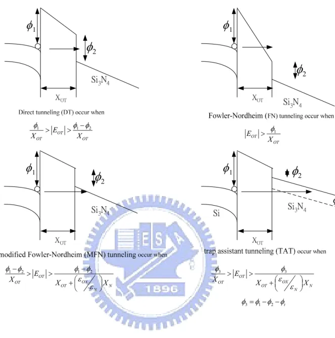
(39) 2.2 Basic Program/Erase Mechanisms. 2.2.1. Carrier Injection Mechanisms. The problem of writing an FG cell corresponds to the physical problem of forcing an electron above or across an energy barrier. The problem can be solved exploiting different physical effects [2-1]. The three main physical mechanisms used to write an FG memory cell are sketched. Tunneling is a quantum mechanical process. For nonvolatile memory which has FG on the gate such as SONOS structure, the writing and erasing processes for an n-channel semiconductor memory device are illustrated schematically in Fig. 2-2. During the writing process, a positive gate voltage is applied to inject channel inversion-layer electrons into the nitride layer. I could talk by the same token. During the erasing process, a reverse gate bias is applied to cause the electrons to tunnel back into the channel and the accumulation layer holes to tunnel into the nitride from the channel. There are many ways to achieve “programming” or “erasing”. Tunneling through the oxide can be attributed to different carrier-injection mechanisms. Which process applies depends on the oxide thickness and the applied gate field or voltage. In general, hot carrier electron injection (CHE) and tunneling injection are two kinds of common operation mechanism employed in novel nonvolatile memories. Tunneling injection methods includes. direct. tunneling,. Fowler–Nordheim. (FN). tunneling,. Modified. Fowler–Nordheim tunneling (MFN) and trap assistant tunneling (TAT). These are the main programming mechanisms employed in memory [2-2] to [2-4]. They were showed in Fig. 2-3.. 21.
(40) Ec Ev Si substrate SiO2. Si3N4 SiO2. +V Gate. (a) write mode. Ec Ev. -V Gate Si3N4. SiO2. +. Si substrate SiO2. (b) erase mode Figure 2-2. Memory band diagram in (a)write mode (b)Erase mode. 22.
(41) φ1. φ1. φ2 φ2. φ1 X OT. > EOT >. φ1. φ1 − φ2. EOT >. X OT. φ1 X OT. φ1. φ2. φ2 φt. φ1 − φ2 X OT. > EOT >. X OT. φ3. φ1 − φ2 ε + ⎛⎜ OX ⎞⎟ X N εN ⎠ ⎝. X OT. > EOT >. φ3. X OT. ε + ⎛⎜ OX ⎞⎟ X N εN ⎠ ⎝. φ3 = φ1 − φ2 − φt. Figure 2-3. Fourth approaches to programming methods, described by. Hu and White (Ref. Amit K. Banerjee, Yin Hu, Matthew G. Martin and Marvin H. White, An Automated SONOS NVSM Dynamic Characterization System, 0-7803-1290-N3 $3.00 01993 IEEE). 2.2.2. Channel Hot Electron (CHE) Injection Channel hot electron (CHE) [2-5] injection is widely used as programming. method in nonvolatile memories (NVM), especially in floating-gate [2-6] and. 23.
(42) NROMTM [2-7] [2-8] devices. The physical mechanism of CHE injection is relatively simple to understand qualitatively. An electron traveling from the source to the drain have gained very high kinetic energy after being accelerated by a strong electric field in areas of high field intensities within a semiconductor (especially MOS) device. At low fields, this is a dynamic equilibrium condition, which holds until the field strength reaches approximately 105V/cm [2-9]. For fields exceeding this value, electrons are no longer in equilibrium with the lattice, and their energy relative to the conduction band edge begins to increase. Because of their high kinetic energy, hot carriers can get injected and trapped in areas of the device where they shouldn't be, forming a space charge that causes the device to degrade or become unstable. Electrons are “heated” by the high lateral electric field, and a small fraction of them have enough energy to surmount the barrier between oxide and silicon conduction band edges (electrons need about 3.1eV). In the other hand, the effective mass of hole is heavier than one of electron. It is too hard to obtain enough energy to surmount oxide barrier. Therefore, hot-hole injection rarely is employed in nonvolatile memory operation.. 2.2.3. Fowler–Nordheim (FN) Tunneling. Fowler-Nordheim (FN) tunneling mechanism is the process whereby electrons tunnel through a barrier in the presence of a high electric field and occurs when applying a strong electric field (in the range of 8-10 MV/cm) across a thin oxide. In these conditions, the energy band diagram of the oxide region is very steep. Fowler-Nordheim (FN) tunneling mechanism is based on the quantum mechanical process which is an important mechanism for thin barriers. The tunnel probability that we derived from the time independent Schrödinger equation is 24.
(43) ⎡ L 2m* [V ( x) − E ] ⎤ Ψ ( L) = Ψ (0) exp ⎢ − ∫ dx ⎥ = ⎢ 0 ⎥ ⎣ ⎦ The minus sign is chosen since we assume the particle to move from left to right. For a slowly varying potential the amplitude of the wave function at x = L can be related to the wave function at x = 0. This equation is referred to as the WKB (Wentzel-Kramers-Brillouin) approximation [2-10]. Using a free-electron gas model for the metal and the WKB approximation for the tunneling probability, one obtains the following expression for current density [2-11]. The tunneling probability, Θ , can be written ⎡ 4 Θ = exp ⎢⎢ 3 ⎣. * φB3/2 ⎤ 2qmOX ⎥ h E ⎥. ⎦. the electric field equals E = B/L B is the barrier height ∗ mOX is the effective mass of the electron in the forbidden gap of the dielectric. =. is the Planck’s constant,. q. is the electronic charge,. E. is the electric field through the oxide.. The carrier density equals the density of available electrons multiplied with the tunneling probability, yielding:. J = nqVRΘ ∝ φB3/ 2 The tunneling current therefore depends exponentially on the barrier height to the 3/2 power. However, the exponential dependence of tunnel current on the oxide-electric field causes some critical problems of process control because, for example, a very small variation of oxide thickness among the cells in a memory array produces a great 25.
(44) difference in programming or erasing currents, thus spreading the threshold voltage distribution in both logical states.. 2.2.4. Direct Tunneling (DT). It occurs below ≈ 5nm and with such a thin insulator or other phenomena such as quantum effects cannot be ignored. For nanocrystal memories, the control-gate coupling ratio of nanocrystal memory devices is inherently small [2-12]. As a result, F-N tunneling cannot serve as an efficient write/erase mechanism when a relatively thick tunnel oxide is used, because the strong electric field cannot be confined in one oxide layer. The direct tunneling is employed in nanocrystal memories instead. In the direct-tunneling regime, a thin oxide with thickness less than 3~5 nm is used to separate the nanocrystals from the channel. During write/erase operations, electrons / holes can pass through the oxide by direct tunneling, which gives the advantages of fast write/erase and low operation voltage. In the other hand, the direct tunneling is more sensitive to the barrier width than barrier height, two to four orders of magnitude reduction in leakage current can still be achieved if large work function metals, such as Au or Pt.. 2.3 Basic Physics Characteristics of Nanocrystal Memory. 2.3.1. Quantum Confinement Effect. The study of nanometer-size effects in direct gap semiconductor crystallites is an active field. In this size range, three-dimensional quantum confinement completely changes the optical and electronic properties of these nanocrystals compared to those of the bulk. The band gap increases with decreasing diameter, and the excited 26.
(45) electronic states become discrete with high oscillator strength and therefore it dependence on nanocrystal size has been studied both experimentally and theoretically with the tight-binding model. However, there is little experimental understanding of the basic nature of confinement for indirect gap materials such as silicon [2-13], despite strong theoretical interest. Silicon confinement contains new physics as well as possible technological importance. Confinement could enhance band gap luminescence [2-14 to 2-16], which is forbidden in bulk material, possibly enough to enable laser or display applications. However, a quantitative characterization of this enhancement in real nanocrystals has not been explored. Compared with bulk Ge, a 3nm Ge nanocrystal can have a conduction band shift of 0.5eV, which is significant enough to affect the electrical performance of the nanocrystal memory cell.. 2.3.2. Coulomb Blockade Effect. Coulomb blockade was first observed in tunnel junctions containing a small metallic particle [2-17].The stored electron charge will raise the nanocrystal potential energy and reduce the electric field across the tunnel oxide, resulting in reduction of the tunneling current density during the write process. It is showed in Fig. 2-4.The Coulomb blockade effect can effectively inhibit the electron tunneling at low gate voltage and improve the flash memory array immunity to disturbance. However, the Coulomb blockade effect should be reduced by employing large nanocrystals if large tunneling current and fast programming speed is desired. The Coulomb blockade effect has a detrimental effect on the retention time, since the electrons in the nanocrystal have large tendency to tunnel back into the channel if the nanocrystal potential energy is high in retention mode. Another, the quantum confinement energy shifts the nanocrystal conduction band edge upward so that the conduction band offset 27.
(46) between the nanocrystal and the surrounding oxide is reduced.. Figure 2-4. Coulomb blockade effect. 28.
數據
+7


相關文件
The first row shows the eyespot with white inner ring, black middle ring, and yellow outer ring in Bicyclus anynana.. The second row provides the eyespot with black inner ring
Reading Task 6: Genre Structure and Language Features. • Now let’s look at how language features (e.g. sentence patterns) are connected to the structure
• helps teachers collect learning evidence to provide timely feedback & refine teaching strategies.. AaL • engages students in reflecting on & monitoring their progress
Robinson Crusoe is an Englishman from the 1) t_______ of York in the seventeenth century, the youngest son of a merchant of German origin. This trip is financially successful,
fostering independent application of reading strategies Strategy 7: Provide opportunities for students to track, reflect on, and share their learning progress (destination). •
Strategy 3: Offer descriptive feedback during the learning process (enabling strategy). Where the
How does drama help to develop English language skills.. In Forms 2-6, students develop their self-expression by participating in a wide range of activities
Now, nearly all of the current flows through wire S since it has a much lower resistance than the light bulb. The light bulb does not glow because the current flowing through it
