晶圓打線檢測系統之研究
Automatic Inspection System Design for Wire Bonding
研 究 生:周正全
Student: Cheng-Chuan Chou
指導教授:彭德保 博士
Advisor: Dr. Der-Baau Perng
國立交通大學
工業工程與管理學系
博 士 論 文
A Dissertation
Submitted to Department of Industrial Engineering and Management College of Management
National Chiao-Tung University in Partial Fulfillment of the Requirements
for the Degree of Doctor of Philosophy in Industrial Engineering and Management
October 2006
Hsinchu, Taiwan, Republic of China
摘要
在半導體產業中,晶圓封裝往往被認為是技術層次較低的一環。然而由於半導體 線寬走向0.1 微米以下製程,封裝已成為良率的瓶頸。在晶圓封裝過程中,打線是最 精密,最複雜,也是最容易發生錯誤的製程。客戶在評估封裝廠能力時,打線的品質 是最大的重點。在打線製程中,必須對金線及金線球的位置、線弧高度和形狀等進行 詳細的檢驗,一但發生錯誤則會造成大量的報廢及損失。目前封裝廠絕大多數是以人 工對打線完成之半成品進行抽檢,然而人工目視不但容易失誤且耗時過久,勢必無法 滿足未來客戶100%品檢的要求。 本論文的目的,在發展出一套適用於封裝廠打線製程的電腦視覺檢測系統,能檢 測出已知所有可能會發生的錯誤,包括漏線、線偏、斷線、短路和線塌。金線由於線 徑極細加上背景之晶圓及導線架反射性高,造成從上視角取像的二維影像中,不易對 金線進行定位及檢測。因此本論文先對金線及金線球的反射特性進行分析研究。並以 此為依據,發展出一套可自動程式控制光線入射角的結構光源系統。使用此一結構光 源系統,金線的位置資訊將能清晰的表現在二維檢測影像中,因此漏線、線偏、斷線 及短路現象都能有效的被觀測。而本論文將立體線塌瑕疵的檢測方法,由傳統的高度 量測轉換為斜率檢測;以程式精密的控制光線入射角範圍大小,使立體的線塌瑕疵也 能被突顯在二維的檢測影像中。 本論文並開發出一系列的演算法,能快速且有效的檢測出所有打線製程中的瑕 疵。經由實驗結果可證明,本論文提出之金線檢測系統,其檢測速度遠高於目前現有 之打線機台。此檢測系統將可應用於實際晶圓打線生產線,達成100%全檢的目標。 關鍵字:自動光學檢測;晶圓封裝;結構光源II
-Abstract
Wire bonding is the process that makes the connection between the IC chip and the substrate. The minimum diameter of a bonding wire, which appears as a 3D loop in an IC chip, is about 20 μm. This kind of bonding wire easily bends or sags in the middle segment. Bonding wire defects can be classified as 2D-type and 3D-type. The 2D-type defects include broken, lost, shifted or shorted wires. These defects can be inspected from a 2D top-view image of the wire. The 3D-type defect is wire sagging, which is difficult to be inspected from a 2D top-view image.
In this dissertation, a structured lighting system was designed and developed to facilitate all 2D and 3D-type defect inspection. The devised lighting system can be programmed to turn the structured LEDs on or off independently. For the 2D-type defect, the lighting system can provide light in proper incident angle to illuminate the bonding wire and the position of bonding wire will be represented in the image clearly. For the 3D-type defect, we supplant the traditional height measurement by the slope inspection. The structured lighting system can provide light in proper incident range and the variance of slope, the sagged wire segment, will be highlighted in a 2D image. Experiments show that the devised illumination system is effective and robust for wire bonding defect inspection.
We developed a fast and robust set of machine vision algorithms for wire bonding inspection. The defect of a bonding wire being broken, lost, shifted, shorted or sagged in an IC chip can be inspected automatically. Some illustrations are given to show the efficiency and effectiveness of this proposed novel wire bonding vision inspection system.
誌謝
首先感謝 彭德保教授在我博士班六年期間給予的指導與鼓勵,老師的專業素養與 行事風格,都將是我學習的目標。在實驗所需的器材及其他方面的支援也非常充足, 讓我能順利的完成博士班的研究。感謝各位口試委員提供的寶貴意見,使這篇博士論 文能更為完善。 感謝李恕明同學從研究的初期,就不斷提供許多實驗用的樣本以及專業的意見,讓 我的研究能與實務有最密切的結合。感謝實驗室的學弟妹們,在帶領大家一起成長的 過程中,我也得到許多寶貴的經驗。這些相處的過程,都將會是我未來繼續研究的最 大資產與動力。 感謝多年來提供我們許多研究計畫的廠商們,有了你們的大力支持,我及實驗室才 會不斷的成長。感謝曜宇科技公司的協助,使得研究中最關鍵的結構光源能順利製作 完成,其完成度與實用性也受到大家一致的好評。特別感謝國科會歷年來所撥予的研 究經費補助,使本研究能順利的進行。 最後要謝謝我的父母及家人,在我博士班的過程中不斷的給我支持與鼓勵,讓我專 心的在研究的路上不斷前進。我能取得博士學位是因為有大家的付出,與你們共享這 份成果與喜悅。 周正全 於交通大學工業工程與管理系電腦視覺實驗室 民國九十五年十一月IV
-Contents
摘要 ... I Abstract ...II 誌謝 ... III Contents... IV List of Figures ... VI List of Tables ... X 1. Introduction ... 11-1 Introduction to the problem...1
1-2 Objectives...4
1-3 Organization of the dissertation ...6
2. Surveys... 7
2.1 Literature review...7
2.2 Surveys of lighting device ...9
3. Reflection Models ... 13
3.1 Reflection model of bonding ball ...14
3.2 Reflection model of bonding wire...15
4. Structured LED Lighting System for Bonding Wire Inspection ... 22
4.1 Concept and prototype of the structured LED lighting system ...22
4-2 Illumination effect for 2D wire inspection...26
4-3 Illumination effect for 3D wire inspection...27
5. Inspection Algorithms ... 35
5-1 Bonding ball inspection...38
5-2 Shorted wire inspection...41
5-4 Shifted wire inspection...45
6. Experimentation and Result Analysis... 49
6-1 Experimental environment setting ...49
6-2 Experimental result of bonding ball inspection...50
6-3 Experimental result of shorted bonding wire inspection...51
6-4 Experimental result of lost wire inspection...54
6-5 Experimental result of broken wire inspection ...56
6-6 Experimental result of sagged Wire Inspection...57
6-7 Experimental result of shifted wire inspection...58
7. Conclusions and Further Studies ... 62
7-1. Conclusions ...62
7-2 Contributions...62
7-3 Further Studies ...63
VI
-List of Figures
Figure 1. The diagram of IC chips with bonding wires on the substrate...2
Figure 2. Illustrative and enlarged image of a wire bonded IC ...2
Figure 3. Illustration of good bonding wire...3
Figure 4. Illustration of five possible bonding wire defects ...3
Figure 5. The flow chart of packaging process ...4
Figure 6. Illustration of the incident angle of a circular fluorescent light with surrounding ring diameter of 70 mm and tube height of 17mm. The incident light angle ranges from 17 o to 35 o... 9
Figure 7. The illustration of a dome-type LED lighting device ...10
Figure 8. Illustration of the linear inclined optical fiber...10
Figure. 9. The grabbed image histogram for the linear inclined optical fiber... 11
Figure 10. Illustration of simplified reflection model ...13
Figure 11. The illustration of (a) the reflection model and (b) the highlighted region of the bonding ball ...15
Figure 12. (a) The illustration of the setting of the ring type fluorescent light source for bonding ball illumination and (b) the grabbed bonding ball image ...15
Figure 13. (a) Illustration of the track of the capillary of bonding machine and (b) side-view illustration of the 3D actual loop of a bonding wire connecting the pad and lead ...16
Figure 14. Illustration of four independent light sources, each is designed to illuminate one of the four sided bonding wires of an IC chip ...18
Figure 15. Illustration of the bonding wires located along one side of the IC chip (a) with different deflection angles and (b) with different slopes ...19
Figure 16. The stereograph of a pseudo wire surface formed by the bonding wires in one side of an IC chip...20
Figure 17. (a) A side-view of the proposed structured lighting system. For clarity, only the east and west strips of LED arrays and associated soft PCBs are depicted. (b) A 3D illustration of the structured lighting system (c) A photograph of the prototype of the proposed structured LED lighting system ...23
Figure 18. An illustration of the inaccuracy of incident light angle of the structured LED lighting system...25 Figure 19. The image of bonding wires grabbed using the structured LED lighting system (a) all good wires (b) some shifted wires...27 Figure 20. Profile of the tested good bonding wire with the slope of 20 degree...28 Figure 21. The gray-level of the pixels on the bonding wires of the grabbed images in Table
3 when (a) 16th, (b) 17th, (c) 18th and (d) 19th row of LEDs was turned on...31 Figure 22. Profiles of (a) the slightly sagged wires with a drop of 24 degree in slope and (b)
the seriously sagged wires with a drop of 28 degree in slope ...33 Figure 23. The flowchart of the developed AOI system for image grabbing and bonding
wire inspection...37 Figure 24. Images of the bonding ball with variant shapes of contour ...39 Figure 25. Illustration of the projection regions for (a) a pair of normal wires and (b) a pair
of shorted wires. The red rectangular regions indicate the projection regions and the project directions are set as parallel with the wires. ...42 Figure 26. Illustration of the scan lines for lost/broken/sagged wire inspection. The red lines
indicate the scan lines of (a) a normal wire (b) a lost wire (c) a broken wire and (d) a sagged wire ...44 Figure 27. Illustration of scan lines for shifted wire inspection with one diameter specification of (a) a normal wire, (b) a wire shifted away by 0.5 * diameter, (c) a wire shifted away by 1 * diameter, (d) a wire shifted away by 1.5 * diameter and (e) a wire shifted away by 2 * diameter ...46 Figure 28. Illustration of scan lines for shifted wire inspection with one and half diameter
specification of (a) a normal wire, (b) a wire shifted away by 0.5 * diameter, (c) a wire shifted away by 1 * diameter, (d) a wire shifted away by 1.5 * diameter and (e) a wire shifted away by 2 * diameter ...47 Figure 29. The illustration of experimental equipments for wire bonding inspection ...49 Figure 30. The synthesized image of the experimental IC chip ...50 Figure 31. The search model of an exemplified bonding ball (19 x 14 pixels, 4.5um/pixel)..51 Figure 32. The detected results of bonding balls of the images as shown in Figure 24. The
ball with a cross-hair mark means it was found by the proposed pattern matching method. ...51
VIII
-Figure 33. (a) The grabbed image of bonding wires and (b) binarized image with μ+3σ of the gray-level of background as the threshold and (c) binarized image with μ+6σ of the gray-level of background as the threshold...52 Figure 34. Experimentation of shorted wire inspection: (a) The grabbed image of the
bonding wires in the north side of IC chip without shorted defect (b) the image with a man-made shorted defect. The meshed rectangular regions indicate the projection regions and the chart in (c) and (d), respectively, illustrates the projection result of Figures 34(a) and 34(b). The squares indicate the accumulative gray-level of the projection region and the horizontal lines indicate the threshold value of the background. ...53 Figure 35. Experimentation of lost wire inspection: (a) The grabbed image of the normal
bonding wires in the north side of IC chip and (b) the image with a man-made lost defect in the 6-th bonding wire from the right. The horizontal lines indicate the scan lines for lost/broken/sagged wire defect inspection. The (c) and (d), respectively, illustrates the maximum gray-levels of the wires on the scan lines in Figure 35(a) and 35(b). The squares indicate the maximum gray-levels of scan lines and the horizontal lines indicate the threshold value of the background ...55 Figure 36. Experimentation of broken wire inspection: (a) The grabbed image of a broken
defect in the 5-th bonding wire from the left and the corresponding scan lines for lost/broken/sagged wire defect inspection. (b) the maximum gray-levels of the wire on the scan lines in Figure 36(a), the squares indicate the maximum gray-levels of scan lines and the horizontal line indicates the threshold value of the background ...56 Figure 37. Experimentation of sagged wire inspection: (a) The grabbed image of a sagged
defect in the most left bonding wire and the corresponding scan lines for lost/broken/sagged wire defect inspection. (b) the maximum gray-levels of the wire on the scan lines in Figure 37(a), the squares indicate the maximum gray-levels of scan lines and the horizontal line indicates the threshold value of the background ...57 Figure 38. Experimentation of shifted wire inspection with the allowance in one diameter of
the wire: (a) the image with a shifted bonding wire in the second from the top and the two parallel lines indicate the scan lines for shifted wire defect inspection. We enlarge the middle segment of the wire for clear representation. (b) The gray-level of the pixels on the two scan lines, the squares indicate the gray-levels of the pixels on scan line 1, the dots indicate the gray-levels of the pixels on scan line 2 and the horizontal line indicates the threshold value of the background...59
Figure 39. Experimentation of shifted wire inspection with the allowance in one and half diameter of the wire: (a) the same photo in Figure 38(a) and the three parallel lines indicate the three scan lines for shifted wire defect inspection. The middle segment of the wire is enlarged for clear representation. (b) the gray-level of the pixels on the three scan lines, the squares indicate the gray-levels of the pixels on scan line 1, the dots indicate the gray-levels of the pixel on scan line 2, the triangles indicate the gray-levels of the pixels on scan line 3 and the horizontal line indicates the threshold value of the background ...61
X
-List of Tables
Table 1. Illumination of the effect by using the circular fluorescent, the dome-type LED and the linear inclined optical fiber. ...12 Table 2. The information of single sample bonding wire...17 Table 3. The images of a single bonding wire grabbed by turning on some of the LEDs of
the developed structured LED lighting system...29 Table 4. The images of a single bonding wire grabbed for 3D wire inspection by turning on
1. Introduction
1-1 Introduction to the problem
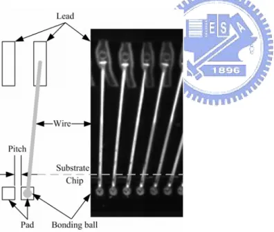
In the IC manufacturing process, the wafers are diced as the IC chips after the processing and wafer-level testing steps are completed. In the packaging process, the wire bonding makes the connection between the IC chip and the substrate. Because the original connecting areas of an IC chip are too small to be welded on the PCB, some kind of substrate is devised and used as the connecting medium between the IC chip and the PCB. In this technique, the backside of the IC chip is first glued down on the substrate. Later the bonding machine attaches individual wires between the IC chip connections and the substrate. The connector on an IC chip is called the pad, the interval between two adjacent pads is generally referred to as the pitch and the connector on the substrate is called the lead. Typically, a high purity gold wire or aluminum wire is used to connect the pad and the corresponding lead. Aluminum has good metallurgical properties, but its electrical resistance is higher than gold, making it less desirable for high-speed packaging applications. Nowadays, the gold wire is used mostly in the packaging process. Some features of the bonded aluminum wire are dissimilar with golden wire and this dissertation will focus only on the inspection of bonded IC by using golden wire. The wire bonding process consists of the following four steps. (1) The bonding machine uses hydrogen flame or electronic spark to form a ball on the tail of the wire. (2) The capillary of the bonding machine targets on the center of the pad descends and brings the ball in contact with the pad. Ultrasound vibration is applied to assist the welding at the same time. (3) Once the ball was bonded on the pad, the capillary moves to the corresponding lead in the predefined track. The wire is fed out from the end of the capillary to form a loop. (4) The capillary deforms the wire against the lead and produces a wedge-shaped bonding stitch on the lead. The image of a whole chip with about 100 surrounding wires is shown in Figure 1. Part of the
2
-enlarged wire bonded IC image is illustrated in Figure 2.
Figure 1. The diagram of IC chips with bonding wires on the substrate
Figure 2. Illustrative and enlarged image of a wire bonded IC
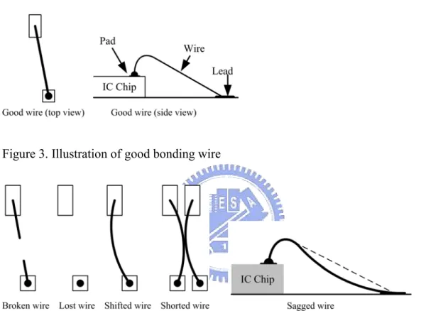
The minimum diameter of a bonding wire, which appears as a 3D loop in an IC chip, is about 20 μm. Such kind of bonding wire is easy to bend or sag in the middle segment. The bonding machine may place the bonding ball in wrong position to cause shifted wire. The outer force may bend the bonding wire to cause defect. The gravity or other forces may
cause a 3D sagging in the bonding wire which is generally named as a sagged wire. The defects that may occur on the bonding wire can be classified into 2D type and 3D type. The objective of 2D type defect inspection is to detect whether any wire is missed, shifted or shorted and the 3D type defect inspection focuses on the sagged wire. Figure 3 and Figure 4 respectively illustrate a good wire and possible defects of bonding wire.
Figure 3. Illustration of good bonding wire
Figure 4. Illustration of five possible bonding wire defects
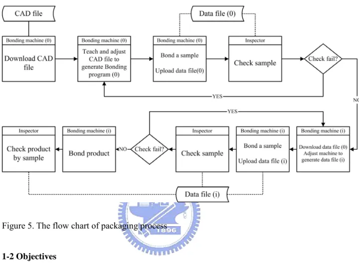
Currently, the human inspectors check the quality of bonded wires on a sampled basis by using a microscope. Figure 5 illustrates the flow of packaging and the human inspection process. The inspectors must check the samples and products of bonding machine. It is hard and inefficient for human eyes to collate the actual defective position of bonding wires. So, an automatic optical inspection (AOI) system is required and helpful to check the wires of a chip. The AOI system can check the position of bonding ball by using the bonding program
4
-and can detect all the defects of bonding wire on the bonded IC chip to ensure the quality of packaging process.
Figure 5. The flow chart of packaging process
1-2 Objectives
The major objective of this dissertation is to develop a bonding wire AOI system, including the hardware and software. The hardware of the proposed AOI system includes the illumination module, image capturing module and loading module, while the software of the proposed AOI system includes the inspection algorithms and the controlling module. This dissertation focuses on the illumination module and the inspection algorithm. After the bonding process, the proposed AOI system can load the bonded IC chips on a substrate and check the quality of bonding balls and wires prior to the next process. The AOI system has to also provide teaching phase module for the tested IC chip inspection.
Due to the tiny diameter, the 3D loop of the bonding wire and the complex background of substrate, it is hard to grab clear image of the bonding balls and bonding wires. That is, a well-designed lighting system that will illuminate the bonding ball and wire more than the background is required for the inspection. To find a suitable lighting system for illuminating the bonding ball and wire, we first analyze the reflection models of the bonding ball and wire. Then the requirements about how to illuminate the bonding ball and wire can be derived from the reflection models. We test three kinds of available lighting devices for illuminating the bonding ball and wire. Then, we developed a new structured LED lighting system that meet the requirement of general bonding wire inspection, especially for the 3D type of sagged defect.
After developing the structured LED lighting system, we develop the inspection algorithms in consequence. The image capturing module extracts consecutive images for the bonding balls and wires on the IC chip and generate four images for inspection. One image covers all the bonding balls and wires on single boundary of the IC chip. These images will be inspected in the next step. There are three focal points in the inspection system: (a) the position of the bonding ball, (b) the position of the bonding wire and (c) the height of the bonding wire. The first focus of the proposed vision inspection system is the position of each of the bonding balls. The bonding ball should normally be placed in the center of the pad. But, either the human operator or the bonding machine may cause some error in positioning the bonding ball. In addition, the size of the IC chip, pad and pitch is getting smaller and smaller, making it more difficult for the human inspector to inspect the position of the bonding ball. Even a slight shift of the ball position may cause an electrical short in the two adjacent pads. We developed a ‘modified pattern matching method’ to get and inspect the position of the bonding ball accurately and quickly.
6
-the bonding wires. To filter out any possible error in -the wire bonding process, a set of associated inspection algorithms were also proposed.
The third focus of the proposed vision inspection system is the height of each of the bonding wires. A sagged wire is very hard to be detected from a top-view 2-D image. With the proposed lighting environment, the AOI system can detect the sagged wire by inspecting the gray-level variation of the bonding wire. By using the proposed illumination system and inspection algorithms, we can develop an AOI system to detect out all the possible defects in the bonding process.
1-3 Organization of the dissertation
This dissertation is organized as follows. In section 2, a survey of related papers and lighting devices are presented. The reflection models of bonding ball and wire are described in section 3. In section 4, the structured lighting system for wire bonding inspection is represented. The section 5 illustrates the algorithms for bonding ball and wire inspections. The experimental environment and result are given in section 6. Finally, the conclusions and further studies are given in section 7.
2. Surveys
2.1 Literature review
Ahmed et al. [1] discussed a 2-D inspection system that can check (a) the bonding capillary marks which should not exceed the pad boundary, (b) the scratches on the pad which must not exceed 50 percent of the pad width, and (c) the bonding capillary marks which must not exceed 25 percent of the pad area. The algorithm extracted the capillary marks by using a local threshold method. It also identified the protrusions of the marks beyond the pad boundary by using a morphological filter.
Khotanzad et al. [2, 3] presented an automatic system for inspecting the quality of the bonding ball which connects the pad and the bonding wire. This system could determine the position of the bonding ball from an ordinary image, which was taken from the top view of an IC wafer, and could extract geometric measures about the contour of the bonding ball. These measures were obtained by using the best-fitting ellipse for the bonding ball. They used the Sobel operator [4] to enhance the original images, and the Otsu’s [5] threshold technique to binarize the enhanced images. The approximate center of the bonding ball was first determined by using a morphological erosion operation. Then the bonding ball contour was found by scanning this center radically. Finally, the parameters of the best-fitting ellipse could be computed by using analytic geometry techniques.
King and Sing [6] presented an algorithm for the bonding wire inspection. There were two main procedures: (a) generating candidate points of the bonding wire, and (b) determining the equation of the bonding wire. They used a one-dimensional gradient threshold technique to generate the “candidate point” of each bonding wire. They treated the “candidate point” as the starting point of the bonding wire. The Hough transformation is used to find out the straight-line equation of the bonding wire. Only (a) missing or extra
8
-wires, and (b) crossing wires were detected by this algorithm.
Zhang et al. [7] developed a visual inspection system for measuring the height of bonding ball by using structured lighting technique. The light source is an incandescent lamp and is being focused twice, through a slit, to form a narrow stripe. The stripe is set at an angle of 45 degree to measure the height of bonding ball from the pad plane. Lim et al. [8] developed a system for bonding ball inspection. The height of the bonding ball was detected by automatically computing the focused planes of both the top and the base of the bonding ball, with a series of 2D images. Nowadays, the bonding machine is precise enough to output the bonding ball of very good and stable height, so the focus is on the bonding wire inspection.
Some studies presented different vision systems which can inspect the position of the bonding wire, and/or the contour and position of the bonding ball. However, none of these vision systems can detect the error in wire height. Ye et al. [9] presented a stereo vision system for wire height inspection. In a single-camera-based setup, stereo views are obtained by rotating the IC chip. They grabbed the first image of the chip and rotated the chip by 180 degree, then grabbed the second image. The edges of the wires are detected by using Petrou’s line filter [10]. The facet model proposed by Haralick and Shapiro [11] is applied to obtain sub-pixel edge localization. Based on the positions of the wires in a pair of images, the height profile of each of the bonding wires was obtained by using a disparity equation derived from the image geometry.
As it is to detect the 3D type defect of bonding wires by using a single 2D image, the illumination system should provide 3D information of bonding wires in a 2D image. Some researchers used structured light for illumination. The 3D shape of the bonding wires was re-constructed by using the features from its 2D image. Wang and Cheng [12] used a slide
projector as the illumination to project a grid pattern onto the object’s surfaces. Woodham [13] proposed a photometric method to recover the surface orientation unambiguously. Some other researchers [14-16] recovered the 3D shape by using photometric method and structured lighting system. But multi-images are required in these researches in order to determine the surface normal.
2.2 Surveys of lighting device
A classical review of lighting system design can be found in Bachelor [17]. Quite a few guidelines and illustrations have been addressed and given. Following that, we have used three lighting devices: circular fluorescent, dome-type LED and linear inclined optical fiber for bonding wire inspection [18]. The incident light angle and its effective range are the two critical factors for lighting device design.
(a) Circular fluorescent light
The circular fluorescent can provide surrounding light in variant incident angle by controlling its setup height. Illustration of a circular fluorescent lighting device is given in Figure 6.
Figure 6. Illustration of the incident angle of a circular fluorescent light with surrounding ring diameter of 70 mm and tube height of 17mm. The incident light angle ranges from 17 o to 35 o
10
-(b) Dome-type LED
The dome-type LED can provide surrounding light in a large range of incident angle, as shown in Figure 7.
Figure 7. The illustration of a dome-type LED lighting device
(c) Linear inclined optical fiber
The linear inclined optical can provide the light in controllable incident angle and range, as shown in Figure 8.
Figure 8. Illustration of the linear inclined optical fiber
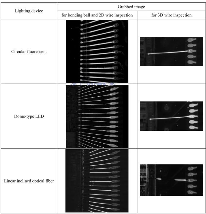
By using three lighting devices in this study, many bonding wire images were grabbed and summarized in Table 1. The lighting devices were set up in experiential proper positions
to achieve optimal illumination. The second column of Table 1 shows three images for bonding ball and 2D wire inspections. By using circular fluorescent and dome-type LED, the grabbed images represent the position of bonding balls and wires clearly. The grabbed image by using linear inclined optical fiber only represents the position of wires clearly. In these high contrast images, we can easily distinguish the bonding wires from the background by a pre-defined threshold. Figure 9 shows the histogram of the grabbed image using linear inclined optical fiber. The gray-level of the background in Figure 9 is very low and easily distinguishable. That is, the wire can be separated from the grabbed image using the binary method with a pre-defined threshold, such as 50.
0 2000 4000 6000 8000 10000 12000 14000 16000 18000 20000 1 26 51 76 101 126 151 176 201 226 251 Pixe l cou n t gray-level Figure. 9. The grabbed image histogram for the linear inclined optical fiber
The third column of Table 1 shows grabbed images for 3D wire inspection. An intentionally sagged wire was tested by 3D wire inspection. Of the three types of lighting devices, the grabbed images show that only the linear inclined optical fiber can highlight the 3D sagged defect. The sagging is represented as a gap in the 2D image grabbed using the linear inclined optical fiber and is obvious for inspection. The surrounding light of the circular and dome-type lighting devices erases the sagging feature and these cannot be used for 3D wire inspection.
12
-To inspect the practical bonding wires, this dissertation presents a simplified bonding wire reflection model and a novel lighting system for bonding wire inspection in the following sections.
Table 1. Illumination of the effect by using the circular fluorescent, the dome-type LED and the linear inclined optical fiber.
Grabbed image Lighting device
for bonding ball and 2D wire inspection for 3D wire inspection
Circular fluorescent
Dome-type LED
3. Reflection Models
The surface orientation of the bonding ball and wire will affect its reflection on the grabbed image as the image is formed by the features reflected from both the background and the objects. The features of the bonding ball and wire can be extracted from the grabbed image under well-controlled environment. In Woodham’s research, three or more images are required to derive two orientation of the 3D reflected surface (e.g. dx and dy of surface z =
f(x,y)). In this dissertation, a simplified reflection model of the inspected objects and a
proper lighting system for grabbing clear images of the bonding balls and wires are proposed. Using the developed lighting system, we can have the AOI system to extract and detect possible defects of the bonding ball and wire by only one top-view image.
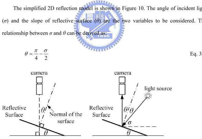
The simplified 2D reflection model is shown in Figure 10. The angle of incident light (σ) and the slope of reflective surface (θ) are the two variables to be considered. The relationship between σ and θ can be derived as:
2 4
σ π
θ = − Eq. 3-1
Figure 10. Illustration of simplified reflection model
Assumed G(x, y) is the gray-level of a pixel in the image which corresponds to a point (x, y) on the reflective surface. When incident light angle is set as σ and the gray value G(x, y) is
14
-greater than a pre-defined threshold, then the slope of reflective surface is θ. That is, we can derive the slope of the reflective surface of the bonding balls and wires from the image grabbed by CCD.
3.1 Reflection model of bonding ball
The bonding ball is the part that links bonding wire and pad. The capillary of bonding machine guides the golden wire in the bonding process. The end of wire is fused on the capillary by using the ultrasonic to form a circular ball first, and then the capillary presses the ball on the pad to form a bonding ball. Because the top-view contour shape of bonding ball will affect the bonding quality of the ball, many researchers focused on the contour shape of bonding ball. The bonding technique is stable enough recently, so the ball’s contour shape can be treated as good enough, and not to be inspected. On the other hand, the interval between adjacent pads is getting closer, a slightly shift of one bonding ball may cause short. So to inspect the bonding ball, the focus is on the ball’s center position. To get the position of bonding ball center, we need the clear contour of every bonding ball in the image. Using the pattern-matching method, we can easily check the position of each bonding ball with the data file.
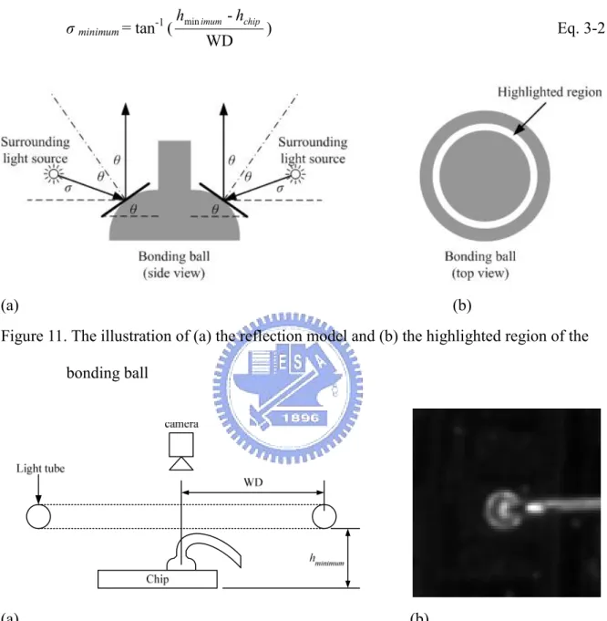
In inspecting the position of bonding ball, the major focus is extracting the ball’s contour. The profile of a bonding ball is of bell-shape, as shown in Figure 11(a), and is surrounding the center of ball symmetrical. That is, if the light is reflected from the ball’s surface with slope θ and the lighting device surrounds the ball, then the complete contour of each of the bonding ball will be obtained in the image, as shown in Figure 11(b). The incident angle of light should be as low as possible and the horizontal surfaces of pads and wafer will not reflect light. We set a lower limit of the incident angle of the light to avoid crash, as shown in Figure 12. And the lowest incident angle σ minimum is calculated by the
working distance (WD), the height of chip (hchip) and the safe-height (hminimum). The
relationship between WD, hchip and hminimum is:
σ minimum = tan-1 (
WD - minimum hchip h
) Eq. 3-2
(a) (b)
Figure 11. The illustration of (a) the reflection model and (b) the highlighted region of the bonding ball
(a) (b)
Figure 12. (a) The illustration of the setting of the ring type fluorescent light source for bonding ball illumination and (b) the grabbed bonding ball image
3.2 Reflection model of bonding wire
The CAD file of bonding wires records coordinates of calibration mark on the substrate and the IC chip, the starting point (pad) and the ending point (lead) of each of the
16
-bonding wires. A -bonding machine searches for a calibration mark first, makes some adjustments, and then bonds gold wires to connect the IC chip with the substrate. When one end of a bonding wire is formed as a bonding ball and is stuck onto a pad, the bonding machine capillary will guide the bonding wire to its corresponding lead on the substrate. The capillary makes the bonding wire hit and connect to the lead, and cuts off the bonding wire at the same time. The track of capillary is designed to form the loop of bonding wire to enhance the wire strength. Factors related to the loop of bonding wire are pad and lead coordinates, loop height, and top length. An illustration of the capillary track is shown in Figure 13(a). An actual bonding wire loop is shown in Figure 13(b).
(a) (b)
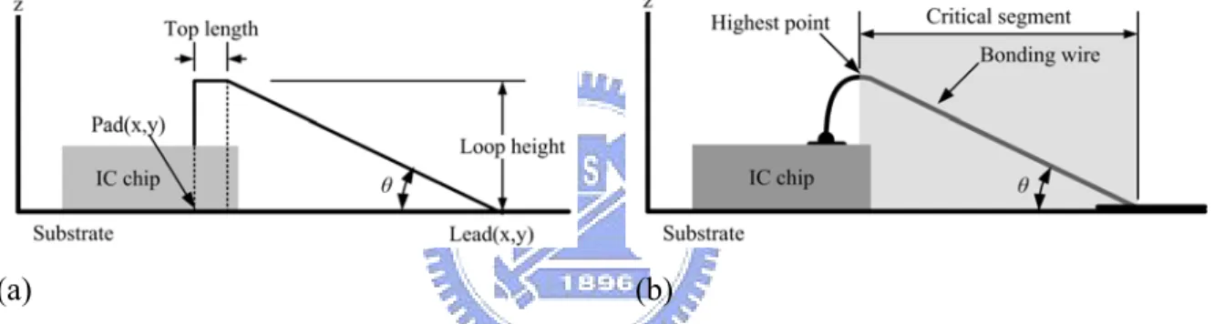
Figure 13. (a) Illustration of the track of the capillary of bonding machine and (b) side-view illustration of the 3D actual loop of a bonding wire connecting the pad and lead In this bonding process, every wire is bonded with a similar slope from the highest point to its corresponding lead. In some cases, the bonding machine may make one or two bends in a longer bonding wire to enhance its strength. Generally, each bonding wire in-between two adjacent bends has a similar slope. For wire inspection, it is necessary to have a clear image of the wire so that the grabbed wire image can be compared to the given data file. To avoid reflection interference caused by the substrate background, only the critical segment of the bonding wire, the segment from the highest point to the lead, is illuminated and inspected. The AOI system can get these factors of wire loop from the CAD data file to calculate the slope of the critical segment. The relationship of the wire slope θ in
the critical segment, the pad and lead coordinates, the loop height and the top length can be represented as Eq. 3-3 below (without bend point).
⎟⎟ ⎠ ⎞ ⎜⎜ ⎝ ⎛ = − length Top -y) Lead(x, y) Pad(x, height Loop tan 1 θ Eq. 3-3
Table 2 shows all the information about single bonding wire on a real IC chip and the calculated slope of critical segment and the proper incident angle of light. Take a wire segment which has the slope of 22.1 degree as an example, by Eq. 3-1, the incident angle of light should be in 45.8 degree to make good reflection. Using the grabbed image, it is possible to detect the position of the bonding wire with a developed AOI system.
Table 2. The information of single sample bonding wire
Factor Pad position (um) Lead position (um) Top length (um) Loop height (um) Slope of critical segment (degree)
proper incident angle of light (degree) data (96.4,1259.4) (-105.3, 1521.1) 45 110 tan-1(110/(330.4-45))
=22.0818
45.8364
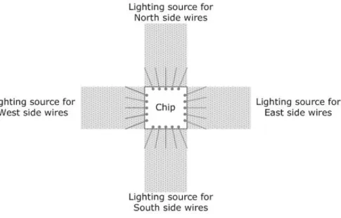
The bonding wires are arranged surrounding the four sides of a chip, and the bonding wires along each side of the chip form a reflective surface. In Section 2.2, the survey of lighting devices indicates that the surrounding light will erase the feature of wire defect. So, we need an independent light source to illuminating each of the four reflective surfaces, as shown in Figure 14. The designed lighting device in such case should provide good enough light to illuminate the bonding wires along one boundary of IC clearly in each grabbed image.
18
-Figure 14. Illustration of four independent light sources, each is designed to illuminate one of the four sided bonding wires of an IC chip
Another reflection model issue is the bonding wire layout. Both the pads and the leads are arranged along the four boundary edges of an IC chip. Because the interval of adjacent pads is smaller than that of leads, bonding wire layout on one side of the IC chip has to be set in a fan-shape, as shown in Figure 15(a). The bonding wire located in the middle has no deflection angle, while the wire closest to the corner of the IC chip has the largest deflection angle and span. As each wire is bonded an the same height, the bonding wire located closest to the corner of the IC chip is longer and has a smaller slope than wires located in the middle. For example, a 1mm high bonding wire with a 0 degree deflection angle and a length of 3mm has a slope of 18.4 degree (inclined slope θ = )
length point highest (
tan−1 ). In
comparison, a 1mm high bonding wire with a 33 degree deflection angle and a length of 3.57mm has a slope of only 15.6 degree, as illustrated in Figure 15(b). To clearly illuminate bonding wires with different slopes or deflection angles, a lighting device must be able to provide light at different incident angles from different directions.
(a) (b)
Figure 15. Illustration of the bonding wires located along one side of the IC chip (a) with different deflection angles and (b) with different slopes
To simplify the bonding wire reflection model, the critical segment of each bonding wire is approximated as a straight line segment. A pseudo reflective surface is a wire surface formed by linking all the highest points of the critical segments, the left-most and the right-most bonding wire, and linking all the associated leads in one side of an IC chip as shown in Figure 16. Once the wire surface is illuminated, all the bonding wires in this surface can be located in the grabbed image. The height and the projected length of the wire surface will decide the incident angle, i.e. the slope θwiresurface, between the pseudo wire surface and the substrate. The θwiresurface is approximately equal to the slope of the bonding wire with a deflection angle of 0 degree. The slope of a pseudo reflective surface can be represented as Eq. 3-4. surface wire θ = tan-1 ( surface wire of length projective surface wire of height ) Eq. 3-4
If the lighting device is set at the incident angle as Eq. 3-1 and Eq. 3-4, all the bonding wires lying on the pseudo reflective surface of the bonding wires can reflect the light with highest intensity into the CCD.
20
-Figure 16. The stereograph of a pseudo wire surface formed by the bonding wires in one side of an IC chip
For 2D-type defect inspection, it is necessary to illuminate and grab the bonding wire first. Practically, a slight slope variance of the critical segment is not treated as a defect. That is, the lighting device should be designed to illuminate the bonding wires with an allowable variance of slope simultaneously. For example, a pseudo wire surface has a slope at 20 degree and the maximum allowable variance of the slope is plus or minus 5 degree (the slope of good wires ranges from 15 degree to 25 degree). The spread range of incident light angle should cover 40 degree to 60 degree to illuminate the wire according to Eq. 3-1. Besides, the critical segment of a bonding wire may contain one or two bends to enhance the strength. Each wire segment between two bend points was in variant slope and we will only illuminate the segment which is next to the lead for wire inspection.
For 3D-type defect inspection, the incident light angle should be spread in an exact range to illuminate the good wires and to highlight the sagged defects at the same time. To illustrate slope variance, the lighting device should provide light in a controllable spread range of incident angle. For example, if the lighting device can provide light with an incident angle of 4 degree, it can illuminate the bonding wire at a slope range of 2 degree. Sagging in the range of plus or minus 1 degree slope can be highlighted for inspection. Since the profile of a bonding wire is a 2D curve, some unexpected reflection and scattering
may exist with a surrounding light source. For 3D wire inspection, the light source should provide suitable light to illuminate the bonding wires at each of the four sides of an IC chip respectively without causing any unexpected scattering.
22
-4. Structured LED Lighting System for Bonding Wire Inspection
Since no any available lighting device fully satisfies the needs of the bonding wire inspection, a structured lighting system for 2D and 3D-type defect inspection was developed, and is presented in this section.
4.1 Concept and prototype of the structured LED lighting system
In 2D-type defect inspection, the light source must provide light with a proper incident angle and large spread range to suitably illuminate the critical segments of bonding wires. While in 3D-type defect inspection, the lighting device should provide light with an exact spread of incident angle so that sagged wires can easily be distinguished from good wires.
To provide suitable light with a controllable incident angle and spread range for each of the four sides of an IC chip without mechanism movement, we designed a prototype structured lighting system containing four LED arrays for this objective. Each LED array was mounted on a soft PCB. The four soft PCBs were fixed symmetrically at the north, south, east and west strips of a hemispheric holder, as shown in Figure 17.
(a)
(b) (c)
Figure 17. (a) A side-view of the proposed structured lighting system. For clarity, only the east and west strips of LED arrays and associated soft PCBs are depicted. (b) A 3D illustration of the structured lighting system (c) A photograph of the prototype of the proposed structured LED lighting system
24
-This configuration matches the four LED arrays with the bonding wires at the four sides of an IC chip. LEDs on different rows can be programmed to turn on or off independently. That is, both the incident light angle and the spread range of the incident light can be totally controlled electronically, highlighted the bonding wires without any mechanical movement. According to Eq. 3-1, the light with a smaller controllable spread range of incident angle can distinguish a slight sagged defect. Both the smaller LED and the larger working distance result in smaller spread range of incident light angle. In the developed prototype, each LED array contains 30 rows of LEDs and the working distance is set at 160mm so that each LED row can provide a fixed 2.5 degree spread range of incident light. Following Eq. 3-1, each row of LEDs in the prototype can illuminate bonding wire with a slope in the range of 1.25 degree. The lowest row is set to provide light at a 6 degree incident angle, so that this row of LEDs is a little higher than the highest point of bonding wire to avoid collision. The number of LEDs on each row can be controlled to provide sufficient light to illuminate the bonding wires within the FOV (field of view) of CCD without unexpected reflection. The size of FOV is decided by the pixel size and the resolution of CCD. To inspect the bonding wire with 20 um diameter, the pixel size of an AOI system must smaller than 5um. The estimated maximum FOV of CCD will be about 10mm x 10mm and the number of LEDs in each row is set to be three.
When the LEDs mounted on the i-th to j-th rows are turned on, the range of slope of the illuminated bonding wire can be calculated using Eq. 4-1. For example, the LEDs on the 5th to 8th rows can illuminate the bonding wires with slopes from
8 5 32 to 8 5 37 degree. ( 90 - upper boundary of incident light angle) * 0.5
< inclined slope of illuminated bonding wire
< ( 90 - lower boundary of incident light angle) * 0.5 That is,
{ 90 - [ 6 + ( j ) – 1 ] * 2.5 + 1.25 ] } * 0.5 < inclined slope of illuminated bonding wire
< { 90 - [ 6 + ( i ) – 1 ] * 2.5 - 1.25 ] } * 0.5 Eq. 4-1 In practice, the incident light angle of LED will not equal to the theoretical value. Not only the wires located in the center of FOV of the CCD will be reflected but also those within the FOV will cause some deviation of the incident light angle, as shown in Figure 18. If an LED is set in θ slope and its incident light angle ranges in Δθ, the actual incident light angle of the LED can be represented as Eq. 4-2.
Figure 18. An illustration of the inaccuracy of incident light angle of the structured LED lighting system ⎟ ⎟ ⎟ ⎟ ⎠ ⎞ ⎜ ⎜ ⎜ ⎜ ⎝ ⎛ × ⎟ ⎠ ⎞ ⎜ ⎝ ⎛ +Δ × = − 2 FOV of width LED of W.D. 2 s LED W.D.of tan 1 max cosθ in θ θ θ ⎟ ⎟ ⎟ ⎟ ⎠ ⎞ ⎜ ⎜ ⎜ ⎜ ⎝ ⎛ + × ⎟ ⎠ ⎞ ⎜ ⎝ ⎛ Δ − × = − 2 FOV of width LED of W.D. 2 s LED W.D.of tan 1 max θ θ θ θ cos in Eq. 4-2
26
-For example, if the width of FOV is the maximum estimated value of 10mm, the actual incident light angle of the 11-th row of LEDs will range from 28.19 to 31.85 degree. The difference between actual and theoretical value, from 28.75 to 31.25 degree, will only result in small extension of reflective segment of the bonding wire. Such deviation of the incident light angle will be neglected in the following part of the dissertation to simplify the description.
In Section 2.2, three types of lighting device were tested for 2D and 3D bonding wire inspection. In this section, the illumination results of the structured LED lighting system will be presented. In Section 4.2, the structured LED lighting system was set to provide light with a proper incident angle and spread range to illuminate the critical segments of bonding wires on one side of the IC chip for 2D wire inspection. In Section 4.3, the structured LED lighting system was tested for 3D wire inspection. Three IC chips with good, slightly sagged and seriously sagged bonding wires were used as test samples. These IC chips were specially bonded and only one wire was bonded in one boundary for grabbing the profile of wires. For 2D wire inspection, the LED was set to provide light with a proper incident angle and spread to illuminate the critical segment of bonding wire. For 3D wire inspection, the structured LED lighting system was set to distinguish the good, slightly sagged and seriously sagged bonding wires.
4-2 Illumination effect for 2D wire inspection
When the slope of bonding wire surface was obtained from the CAD data, the LEDs on proper rows were turned on, according to Eq. 3-3, to provide good illumination. For example, the slope of the bonding wire surface of the 2D sample IC is around 32 degree, as shown in Figure 19. The proper incident light angle should be 26 degree and the LEDs on the 5th to 13th rows of the developed structured lighting system were turned on. These
LEDs provides light in the incident angles from 17.25 to 34.75 degree onto the wires. According to Eq. 4-1, all the bonding wires spread in the slope range from 27
8 5
to 36 8 3 degree will be clearly highlighted. The positions of the bonding wires and the 2D-type defects can easily be found from the grabbed images. That is, the structured LED lighting system can illuminate the bonding wires clearly.
(a) (b)
Figure 19. The image of bonding wires grabbed using the structured LED lighting system (a) all good wires (b) some shifted wires
4-3 Illumination effect for 3D wire inspection
According to Eq. 3-1, each row of the structured LED lighting system with an incident angle θ can illuminate bonding wires with a corresponding slope of σ. Figure 20 shows the profile of a good bonding wire and the critical segment which was with the slope of around 20 degree. In Table 3, the first column shows the LEDs in that row was turned on, the second column shows the slope range of the illuminated wire according to Eq. 4-1 and the third column shows the grabbed images by using the structured LED lighting system. First, only one row of LEDs on the structured lighting system was turned on and then more rows were turned on to provide the best illumination. For clarity, the images without illuminated bonding wire can be omitted, when the LEDs on the first to 12th rows and the 22nd to 30th rows were turned on. When the LEDs on the 16th to 19th rows were turned on simultaneously, the mainly critical segment of the bonding wire was illuminated perfectly.