材料科學與工程學系
博 士 論 文
應用在金氧半電晶體之原子層沉積氧化鋁與
砷化銦鎵、砷化銦介面之研究
Study of Atomic Layer Deposition Al
2O
3/InGaAs,
InAs Interfaces for MOSFET Application
研 究 生 : TRINH HAI DANG (金海光)
指導教授 : 張 翼 博士
InAs Interfaces for MOSFET Application
研 究 生:金海光
Student: Trinh Hai Dang
指導教授:張 翼 博士
Advisor: Prof. Edward Yi Chang
國立交通大學
材料科學與工程研究所
博士論文
A Dissertation
Submitted to Department of Materials Science and Engineering
College of Engineering
National Chiao Tung University
In Partial Fulfill of the Requirements
For the Degree of
Doctor of Philosophy
August 2011
Hsinchu, Taiwan, Republic of China
中華民國 一 百 年 八 月
i
本論文集中研究減少 InGaAs 和 InAs 原生氧化層藉由使用數種表面處理和氣體退火條件去 改善原子氣相沉積(ALD)Al2O3/InGaAs, Al2O3/InAs 介面品質。三甲基鋁(TMA)製程及濕
式化學溶液製程這兩種製程的結合與影響被提出。
使用乾式 TMA 來減少 InGaAs, InAs 表面的原生氧化層只有在第一次脈衝有效,接下來便 無效。本研究中指出原生氧化層可以被顯著的移除,藉由使用濕式化學溶液製程,例如 HCl 或 sulfide(硫化物)。然而,結合兩種方法(濕式化學溶液製程與 TMA 預先處理)對於 InGaAs,InAs 表面處理是最為有效的方式。
Al2O3/InAs MOSCAPs 的電性指出對於改善 Al2O3/InAs 介面品質 HCl 加上 TMA 比起 sulfide
加上 TMA 是更有效果的。這個結果是由以下實驗觀察所得:ALD Al2O3 薄膜在 200 。 C 下沉 積。300。 C 下沉積 ALD Al2O3 薄膜再次驗證。同時本研究模擬 Al2O3/InAs 結構在低頻的 C-V。 結果顯示界面缺陷密度(Dit)分佈表現出 U 形在最小的 Dit分佈位於 InAs 傳導帶最低處,i.e. 類施體陷阱在此能隙裡支配。這些類施體陷阱會顯著的減少藉由使用濕式化學溶液製程加 上 TMA 預先處理。 藉由使用濕式化學溶液製程加上 TMA 預先處理和在純氫氣裡沉積 後退火,對於 Al2O3/In0.53Ga0.47As 界面品質有顯著提昇。使用 ex-situ 方法,強力的 C-V 反轉行為第一次被觀 察到在 Al2O3/In0.53Ga0.47As MOSCAP。低 Dit分佈可藉由模擬觀察到,同時模擬及電導法可確 認最小 Dit值 ~10 11 eV-1 cm-2。 Al2O3/InGaAs,InAs 的電性表現不僅受與表面處理方法影響,同時也跟半導體本身性質有 關。這些半導體參數例如:能隙、電子遷移率及 Al2O3/InGaAs 結構的 C-V、I-V 本質濃度特 性都被討論。
ii
This dissertation concentrates on the study of the reduction of InGaAs and InAs native oxides by using several kinds of surface treatments and gas annealing conditions to improve the atomic layer deposition (ALD) Al2O3/InGaAs, Al2O3/InAs interfaces
qualities. Effects of trimethyl aluminum (TMA) treatment, wet chemical surface treatments, and a combination of these two kinds of treatments are investigated.
The use of dry TMA treatment for the reduction of InGaAs, InAs native oxides at surface was only effective in the first pulse and then it became effectless. The study shows that the native oxides could be significantly removed by using wet chemical solution treatments such as HCl or sulfide. However, the combination of wet chemical solution treatments plus TMA pretreatment is the most effective way for InGaAs, InAs surface treatment.
Electrical characterization of Al2O3/InAs MOSCAPs showed that the HCl plus TMA
treatment was more effective in the improvement of Al2O3/InAs interface quality than
that of sulfide plus TMA treatment. This conclusion was observed for the samples which were deposited with ALD Al2O3 films at 200oC and was confirmed again for the samples
deposited with ALD Al2O3 films at 300oC. Low-frequency C-V simulations were
performed for the Al2O3/InAs structures and the extracted interface traps density Dit
profiles present a U-shape with the minimum of the Dit profiles located around the InAs
conduction band minimum, i.e. donor-like traps dominates inside the bandgap. These donor-like traps were significant reduced by using wet chemical plus TMA treatments.
By using the chemical solution plus TMA treatment along with post deposition annealing in pure H2 gas, a significant improvement of Al2O3/In0.53Ga0.47As interface
quality was obtained. A strong C-V inversion behavior was first time observed in Al2O3/In0.53Ga0.47As MOSCAP by using an ex-situ method. Low Dit profile extracted by
simulation was observed and the minimum Dit value of ~1011 eV-1cm-2 was confirmed by
both simulation and conductance method.
The electrical characteristics of Al2O3/InGaAs, InAs not only depend on the surface
treatment methods but also depend on the properties of semiconductors themselves. The effect of semiconductor parameters such as bandgap, electron mobility, and intrinsic concentration on the C-V, I-V characteristics of Al2O3/InGaAs structures are discussed.
iii
The author gratefully acknowledges Chiao Tung University (NCTU), Taiwan and the Compound Semiconductor Device Laboratory (CSD Lab), NCTU, Taiwan for supporting this research.
I firstly would like to express my deep gratitude to my supervisor, Prof. Edward Yi Chang for his guidance, support and patience during my Ph.D time at CSD Lab. I appreciate the freedom in research he provided and the taking care he intended for me at the beginning I joined NCTU. He is always kind to me and his encouragement was a driving force for me in study. I really admire his ability in working and research.
This work could not succeed without the support of some people to them I’d like to give my thanks. I am really indebted to Dr. Lin Yueh Chin, Wong Yuen Yee, Yu Chih Chieh (ITRC), Dr. Kuo Chien I, Nguyen Hong Quan, Dr. Lin Kung Liang, and Tran Binh Tinh for their constant help of experiments and valuable discussions. Thanks to them not only in the research but also the good friendships and the fun they brought to me, especially Yuen Yee, Hong Quan. I also appreciate Dr. Chung Yu Lu, Dr. Chang Chia Ta, Hsieh Yi Fan, Dr. Chang Chia Yuan, Chung Chen Chen, and Chiu Yu-Sheng for their kindly supports of experiments.
Many thanks to my colleagues and good friends including Le Minh Thu, Bui Duc Tinh, Dai Van Truong, Do Thi Hien, Oh Chi Way, Nguyen Chi Lang for the enjoyable times we shared together. Thanks also to my NCTU-FSA team including Maria, Sumer, Martin, Leo, and Korniyenko and NCTU-VSA members for the wonderful extracurricular activities, parties and jolly football matches. My Ph.D. time would be less meaningful without them.
Last but not least, this work dedicates to my dearest parents, my wife and my brothers. I wish to thank to my parents who are always beside me all time and give me a strong hope and belief. Thanks to my wife, Them who has been brought to me the love, happiness and joy. I am so happy to have her in my life. Thanks to my younger brothers, Tat Dat and Trong Duc for their fondness for me. They are also a motive power for me to strive for this work.
iv
DEDICATION
To
My dearest Parents, my Wife, and my Brothers
v Abstract (Chinese) ... i Abstract (English) ... ii Acknowledgment ... iii Dedication ... iv Contents ... v
List of figures ... viii
List of tables... xiv
List of symbols ... xv
List of acronym ... xvii
1. INTRODUCTION ... 1
1.1. An Overview of planar Si-based CMOS Technology ... 2
1.2. High k, metal gate solutions ... 4
1.3. Scaling challengers and future trends ... 9
1.3.1. Scaling challengers ... 9
1.3.2. Future trends ... 10
1.4. III-V compound semiconductors for CMOS technology: motivation, challenges and current progress ... 11
1.4.1. Motivation ... 11
1.4.2. Challengers ... 14
1.4.3. Current progress ... 15
1.5. Problem statement and objective of the dissertation ... 17
1.6. Organization of the dissertation ... 18
References ... 19
2. FABRICATION AND CHARACTERIZATION METHODS ... 25
1.2. Fabrication techniques ... 26
2.1.1. Atomic layer deposition (ALD) ... 26
2.1.2. Electron beam evaporation ... 30
vi
2.3.2. High-resolution transmission electron spectroscopy (HRTEM) ... 39
2.4. Electrical techniques ... 41
2.4.1. Capacitance-voltage (C-V), conductance voltage (G-V) measurements ... 41
2.4.2. Current-voltage (I-V, J-V) measurements ... 45
2.4.3. Conductance and conductance map methods ... 46
References ... 51
3. EFFECTS OF WET CHEMICAL AND TMA TREATMENTS ON THE INTERFACE PROPERTIES IN ALD OF AL2O3 ON INAS ... 52
3.1. Introduction ... 53
3.2. Experiment ... 53
3.3. Results and discussion ... 54
3.3.1 Effect of TMA treatment ... 54
3.3.2. A combination of wet chemical treatments and TMA pretreatment ... 56
3.4. Conclusions ... 60
References ... 61
4. ELECTRICAL CHARACTERIZATION OF AL2O3/N-INAS MOSCAPS WITH VARIOUS SURFACE TREATMENTS ... 64
4.1. Introduction ... 65
4.2. Experiment ... 65
4.3. Results and discussion ... 66
4.3.1. X-ray photoelectron spectroscopy ... 66
4.3.2. Capacitance-voltage characteristics ... 67
4.3.3. Simulation and Dit profiles extraction ... 69
4.4. Conclusions ... 70
References ... 72
5. THE INFLUENCES OF SURFACE TREATMENT AND GAS ANNEALING CONDITIONS ON THE INVERSION BEHAVIORS OF THE ATOMIC LAYER DEPOSITION AL2O3/N-IN0.53GA0.47AS MOSCAP ... 74
vii
5.3. Results and discussion ... 76
5.3.1. Capacitance-voltage characterization ... 76
5.3.2. X-ray photoelectron analysis ... 78
5.3.3. Dit extraction by simulation and conductance methods ... 80
5.4. Conclusions ... 81
References ... 83
6. INVESTIGATION OF ELECTRICAL CHARACTERISTICS OF AL2O3/N-INXGA1-XAS (X =0.53, 0.7) AND INAS CAPACITORS ... 85
6.1. Introduction ... 86
6.2. Experiment ... 86
6.3. Results and discussion ... 87
6.3.1. X-ray photoelectron spectroscopy analysis ... 87
6.3.2. High-resolution transmission electron microscopy micrographs ... 87
6.3.3. Electrical characteristics ... 89 6.4. Conclusions ... 93 References ... 95 7. CONCLUSIONS ... 97 Biography... 99 List of publications ... 100
viii
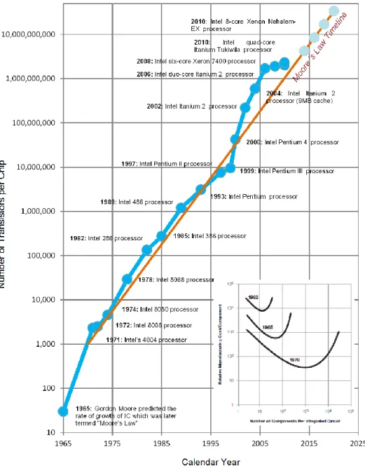
Figure 1.1. “The number of transistors incorporated in a chip will approximately double
every 24 months”: Moore’s Law Timeline (solid) and the number of transistors per chip in Intel’s products (line plus symbols). The inset is Moore’s original prediction graph in 1965... 2
Figure 1.2. Scaling of logic technology node and correspond transistor’s physical gate
length (According to Intel’s introduction until 2009 and ITRS update 2008) ... 3
Figure 1.3. Leakage current versus voltage for various thicknesses of SiO2 layers ... 5
Figure 1.4. At the gate oxide thickness of 1.2 nm (5 layer of atoms), the wave describing
the probable location of an electron is broader than the gate oxide and the electron can simply appear on the other side of gate oxide, means that direct tunneling of electrons through the insulation. New high k gate oxide is needed to plug the leak ... 5
Figure 1.5. Static dielectric constant versus band gap for candidate gate oxides ... 6
Figure 1.6. a-Electron density in PolySi gate is not large enough to screen the effect of
high k dipoles on semiconductor lattice points, lead to strong phonon-electron scattering; b-Experimental evidence of phonon scattering in the high k dielectric. The net value of the temperature (T) sensitivity factor, d(1/eff)/dT, is negative when coulombic scattering
dominates and positive when phonon scattering dominates. [21]; c-Metal gate with high electron density can screen out the vibrations, reduce effect of phonon scattering; d-Experimental (symbols) and simulation (dash lines) data show the improvement of electron mobility by using high k/metal gate stack ... 8
Figure 1.7. The improvements of leakage current and drive currents by using high k
metal gate generations ... 9
Figure 1.8. Illustration of the exponential decrease in switching energy (left) and the
simultaneously increasing device power density (middle) as a consequence of device downscaling. The increase of power density causes of power consumption issue, lowering supply voltage is not an easy way to reduce power consumption due to the increase of off state current, Ioff (right) ... 10
ix
Figure 1.10. Electron velocities as a function of field of Si, Ge and III-V compound
semiconductors. III-V compound semiconductors exhibit high saturation velocity at low electric field ... 11
Figure 1.11. III–V HEMTs characteristics compared with standard silicon MOSFETs a,
Intrinsic gate delay. b, Normalized energy-delay product of n-channel InSb and InGaAs HEMTs ... 14
Figure 2.1. The 8 inch ALD system at instrument technology and research center (ITRC),
Hsinchu, Taiwan. This system was mostly used for the deposition of high k oxides in this work ... 26
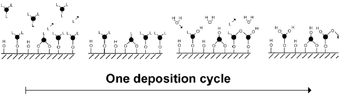
Figure 2.2. Schematic illustration describing an ALD deposition cycle leading to the
formation of a binary oxide film consisting of metal (•) and oxygen (◦) atoms. L refers to the precursor ligand ... 27
Figure 2.3. Schematic describing the alternating TMA and H2O pulses in ALD chamber
leading to form sequence Al2O3 layers ... 28
Figure 2.4. Scheme of (a) ALD processing window limited by (b) precursor condensation,
(c) insufficient reactivity, (d) precursor decomposition and (e) precursor desorption. If deposition rate is dependent on the number of available reactive sites as in (f ), no actual ALD window is observed ... 28
Figure 2.5. Saturation of surface reactions in ALD processes is experimentally verified
by observing that the deposition rate per cycle stabilizes to a constant level with increasing precursor pulse time or dose ... 30
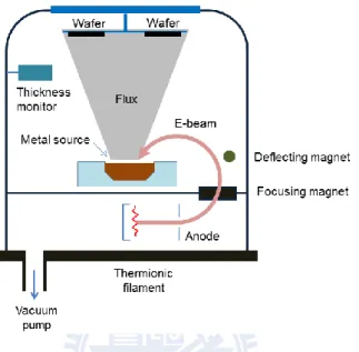
Figure 2.6. Schematic of electron beam evaporation system for metal deposition ... 31
Figure 2.7. The Al2O3/InGaAs, InAs MOSCAPs structures used in this work ... 31
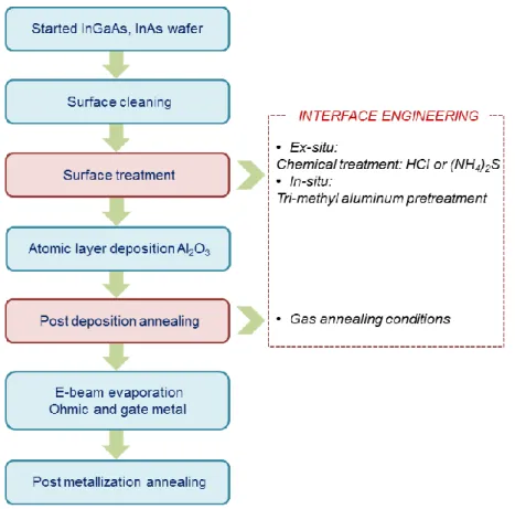
Figure 2.8. Process flow of Al2O3/InGaAs, InAs MOSCAPs fabrication, focusing on the
interface engineering ... 32
Figure 2.9. Surface irradiated by sufficient energy X-ray photon beam will emit
x
state, can reorganize by dropping an electron from a higher energy level to the vacant core hole. (c) Since the electron in (b) dropped to a lower energy state, the atom can rid itself of excess energy by ejecting an electron from a higher energy level. This ejected electron is referred to as an Auger electron. The atom can also shed energy by emitting an
X-ray photon, a process called X-ray fluorescence ... 35
Figure 2.11. XPS survey scan of Al2O3/InAs sample, the inset shows As 3d spectra ... 36
Figure 2.12. Schematic design of an X-ray photoelectron spectrometer ... 37
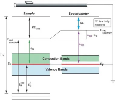
Figure 2.13. The energy level diagram for an electrically conducting sample that is grounded to the spectrometer. The Fermi levels of the sample and spectrometer are aligned (EF(s) = EF(sp) ) so that EB is referenced with respect to EF. The measurement of EB is independent of the sample work function, φs, but is dependent on the spectrometer work function, φsp ... 38
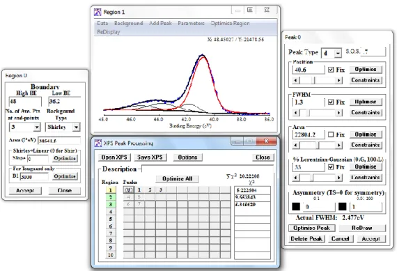
Figure 2.14. The control windows of XPSPEAK software, version 4.1... 39
Figure 2.15. Principle schematic of a transmission electron microscopy (TEM) ... 40
Figure 2.16. Rectangular approximation method used by 4156C ... 43
Figure 2.17. QSCV measurement sequence ... 44
Figure 2.18. Band diagram of an n-type MOS structure with a bias voltage VG applied between metal and semiconductor ... 46
Figure 2.19. Equivalent circuits for conductance measurements: (a) MOSCAP with interface trap time constant τit = RitCit , (b) simplified circuit of (a), (c) measured circuit, (d) including series rs resistance and tunnel conductance Gt ... 47
Figure 2.20. Gp/ versus frequency of an Al2O3/In0.53Ga0.47As MOSCAP device ... 49
Figure 2.21. a-G/Aq as a function of frequency at different gate bias voltages, A is area of MOSCAP; b- G/Aq contours as a function of both frequency and gate voltage, a more efficient and intuitive way to visualize the movement of Fermi level ... 50
Figure 2.22. Characteristic trapping frequencies for electron in n-In0.53Ga0.47As at different temperatures ... 50
xi
cycles (~2 nm) of ALD Al2O3 deposition ... 55
Figure 3.2. XPS As 3d and In 3d5/2 spectra of InAs samples after a-HCl and b-(NH4)2S
treatments and the wet-chemical-treated samples after 10 cycles of TMA pretreatment followed by 20 cycles of ALD Al2O3 (c and d) ... 57
Figure 3.3. Multiple frequency C-V responses and bidirectional curves at frequency of 1
MHz for 10nm ALD Al2O3/n-InAs MOSCAP structures: a-Pure TMA pretreatment,
b-HCl treatment plus TMA pretreatment, c-sulfide treatment plus sulfide pretreatment. The frequency dispersions per decade are 2.3, 1.8, and 2.3% for samples in sequence a to c, respectively ... 58
Figure 3.4. a- C-V responses at frequency of 1 MHz for samples with different surface
treatments. b- Leakage current density versus gate voltage (J-V) of the same samples ... 59
Figure 4.1. The In 3d5/2 and As 2p3/2 XPS spectra of a- native-oxide-covered InAs
surface; b- 1.5 nm ALD Al2O3/HCl+TMA treated InAs interface; c- 1.5 nm ALD
Al2O3/sulfide+TMA treated InAs interface. Native oxides including In2O3, As2O3, and
As2O5 were significantly reduced after the use of surface treatments ... 66
Figure 4.2. Multi-frequency C-V responses (solid lines) and QSCV curves (dashed lines)
in a- control sample, b- HCl plus TMA sample, and c- sulfide plus TMA treated sample of 18 nm ALD Al2O3/InAs MOSCAPs; d- QSCV curves of all three samples, for
comparison ... 67
Figure 4.3. Leakage currents versus gate voltage of samples ... 68
Figure 4.4. a- Experimental data (symbols), simulated C-V curves (solid lines) of ALD
18 nm Al2O3/n-InAs MOSCAP samples with various surface treatments. Interface state
density profiles of all three samples, extracted from simulation, are shown as well: b- control sample, c- HCl plus TMA treated sample, d- sulfide plus TMA treated sample .. 70
Figure 5.1. Multi-frequency C-V responses in a- TMA treated-; b- sulfide + TMA treated
Al2O3/n-In0.53Ga0.47As MOSCAPs, with post deposition annealing in N2 gas. The inset in
xii
dependent C-V responses at 10 kHz of the same sample. The inset in Fig. 5.2a shows the conductance-voltage (G-V) characteristics; the inset in Fig. 5.2b shows the temperature dependent C-V responses at 1 kHz ... 77
Figure 5.3. The As 2p3/2, In 3d5/2, Ga 2p3/2 XPS spectra of a- Native oxide-covered
InGaAs surface; b- TMA treated sample, with ALD Al2O3, as deposited; c- sulfide +
TMA treated sample, with ALD Al2O3, as deposited; d- TMA treated sample, with ALD
Al2O3, after PDA in N2; e- Sulfide + TMA treated sample, with ALD Al2O3, after PDA in
N2; f- Sulfide + TMA treated sample , with ALD Al2O3, after PDA in H2. ... 79
Figure 5.4. a-The comparison of QSCV responses of sample S1, sample S2 and sample
S3 and ideal C-V curve (without Dit) obtained by simulation. The inset shows the leakage
of samples for ensuring the accuracy of measurement; b- and c- The Gp/ - f curves of
sample S1 and sample S2, where Gp is the parallel conductance and is the measured
angular frequency... 80
Figure 5.5. a- Quasi-static C-V data of sample S2 and S3 (symbols) are fitted well with
corresponding simulated data (solids). The ideal C-V curve is also showed as well (dash line); b- “U-shape” Dit profiles of samples S2 and S3 extracted from simulation ... 81
Figure 6.1. a- Parameters of InGaAs compound and schematic of Al2O3/n-InGaAs
MOSCAPs structures with the In content is 0.53, 0.7, and 1; b- Summary of process flow for MOSCAP fabrication ... 87
Figure 6.2. As 3d and In 3d5/2 XPS spectra of (a) native-oxide-corvered InAs surface and
(b) 1.5 nm Al2O3/InGaAs, InAs structures, as deposition. After using surface treatment
and oxide depositon, As-related oxides were reduced to under XPS detection level, the Ga-O and In-O bonds were also significant removed ... 88
Figure 6.3. High-resolution transmission electron microscopy micrographs of 13nm ALD
Al2O3/InGaAs structures after PDA at 400oC in forming gas, showing abrupt
Al2O3/InGaAs, InAs interfaces ... 88
Figure 6.4. Capacitance voltage responses at measured frequency of 1 MHz of
xiii
Figure 6.6. Multi-frequency C-V responses and conductance contours Gp/ (f, V) at
different temperatures (77 K, 180 K and 300 K) of Al2O3/In0.53Ga0.47As. Peaks of
conductance shows the traces of Fermi level movement (solid lines) ... 91
Figure 6.7. Multi-frequency C-V responses and conductance contours Gp/ (f, V) at different temperatures (77 K, 180 K and 300 K) of Al2O3/In0.7Ga0.3As, Al2O3/InAs
MOSCAPs. Conductance contours are closed due to the contribution of inversion layer and thus, the Fermi level traces could not show up ... 92
Figure 6.8. a- leakage current increases with increasing of In content in InGaAs. The
Flower-Nordheim plot for b- Al2O3/In0.53Ga0.47As, c- Al2O3/In0.7Ga0.3As and d-Al2O3/InAs
xiv
Table 1.1. Band gap, bulk carrier mobility, and intrinsic carrier density of Si, Ge and
III-V compounds ... 12
xv
Symbol Unit Description
A m2 Area
Cdep F/m2 MOS capacitance in depletion
Cit F/m2 Interface trap capacitance
Cox F/m2 Oxide capacitance
Cm F/m2 Measured capacitance
Cs F/m2 Semiconductor capacitance
Dit eV-1m-2 Interface trap density, interface states density
E eV Energy difference between a trap and a band
EB eV Electron binding energy
EC eV Conductance band minimum level
Eg eV Semiconductor bandgap
Ei eV Intrinsic energy level
EF eV Fermi level
EV eV Valence band maximum level
0 F/m Vacuum dielectric permittivity
- Relative dielectric permittivity (dielectric constant) of SiO2
k - Relative dielectric permittivity (dielectric constant) of high k
materials
f Hz Frequency
Gp S Parallel conductance
Gm S Measured conductance
Id A, A/m Drain current in a MOSFET
Ig A Gate current in a MOSCAP structure
k J/K Boltzmann’s constant
me kg Electron mass
m* kg Effective electron mass
ni m-3 Intrinsic carrier concentration
NA m-3 Density of acceptor dopant atoms
xvi
NV m-3 Density of states in valence band
Hz Angular frequency
q C Elementary charge
QM C Metal charge in MOSCAP structure
Qs C Semiconductor charge in MOSCAP structure
m2 Trap capture cross section
T K, oC Temperature
tox m Oxide thickness
it s Interface trap time constant
VF V Flat band voltage of MOSCAP
VG V Gate voltage in a MOSCAP
vth m/s Thermal velocity of a charge carrier
, n, p m 2
/V.s Mobility, mobility of electrons and holes
xvii
Symbol Description
ALD Atomic Layer Deposition
ALE Atomic Layer Epitaxy
ALCVD Atomic Layer Chemical Vapor Deposition
CMOS Complement Metal Oxide Semiconductor
C-V Capacitance-Voltage
CET Capacitance Equivalent Thickness
EOT Equivalent Oxide Thickness
ESCA Electron Spectroscopy for Chemical Analysis HRTEM High-resolution Transmission Electron Microscopy
G-V Conductance-Voltage
I-V Current-Voltage
MBE Molecular Beam Epitaxy
MOS Metal Oxide Semiconductor
MOSCAP Metal Oxide Semiconductor Capacitor MOSFET Metal Oxide Semiconductor Transistor
PDA Post Deposition Annealing
PMA Post Metal Annealing
QSCV Quasi-static Capacitance-Voltage
TMA Trimethyl Aluminum
1
Chapter 1
I
NTRODUCTIONThis chapter begins with describing briefly the evolution of semiconductor industry from its commencement to present. Downscaling the parameters of devices according to Moore’s Law is the key feature to continue the development of complementary metal-oxide-semiconductor (CMOS) technology. High k metal gate is a revolutionary change in the CMOS technology up to now. The scaling challenges and future trends in CMOS research are also discussed in this chapter. The motivation, challenges and current progress of high k/III-V MOSFET-one of the possible solution for future CMOS technology, are presented. Finally, the last part of this chapter presents the problems statement of the study on Al2O3/InGaAs interface engineering and the organization of this dissertation.
1.1. An Overview of planar Si-based CMOS Technology ... 2
1.2. High k, metal gate solutions ... 4
1.3. Scaling challengers and future trends ... 9
1.3.1. Scaling challengers ... 9
1.3.2. Future trends ... 10
1.4. III-V compound semiconductors for CMOS technology: motivation, challenges and current progress ... 11
1.4.1. Motivation ... 11
1.4.2. Challengers ... 14
1.4.3. Current progress ... 15
1.5. Problem statement and objective of the dissertation ... 17
1.6. Organization of the dissertation ... 18
2
1.1.An Overview of planar Si-based CMOS Technology
In November 2009, Intel announced that it would state production of microprocessors based on the newest 32 nm generation of logic technology [1]. This latest innovation in semiconductor industry demonstrates the progress of complementary metal-oxide-semiconductor (CMOS) technology from its commencement to present. The progress of semiconductor industry depends closely on the development of the metal-oxide-semiconductor field effect transistor (MOSFET), the key component in integrated circuits.
Figure 1.1. “The number of transistors incorporated in a chip will approximately double every 24
months”: Moore’s Law Timeline (solid) and the number of transistors per chip in Intel’s products (line plus symbols). The inset is Moore’s original prediction graph in 1965 [2].
3
Looking back to the past, the first transistor was invented by Brattain, Barden and Shockley in 1947 and the first integrated circuit was made independently of germanium by Jack Kilby in 1958 and of silicon by Robert Noyce in 1959. The first MOSFET on a silicon substrate was invented by Kahng and Atalla in 1960, 30 years after its principle was proposed by Lilienfield in 1930. Because SiO2/Si interface has very good quality and
stability which allows the fabrication of high performance MOSFET, CMOS technology has been based on the high quality SiO2/Si interface.
In 1965 Electronics Magazine published a paper by Gordon Moore in which he predicted that the number of transistors incorporated in a chip will approximately double every 24 months [2]. This prediction is general known as Moore’s Law (Moore’s original prediction graph is shown in the inset of Fig. 1.1). Moore’s Law has been guiding principle for the semiconductor industry for over 40 years [3], since Intel Corporation was co-founded by Gordon Moore and Robert Noyce in 1968. From that time, by downscaling device feature size, semiconductor industry has passed several generations and made a rapid pace of improvements in its products. Figure 1.1 shows the Moore’s Law time line and the number of transistors per chip of Intel’s products [2, 4]. The transistors per chip doubled after 2-years cadence has been preserved up to now. The number of transistors per chip was thousands in the early-1970s and has increased rapidly to billions recently.
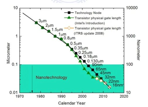
Figure 1.2. Scaling of logic technology node and correspond transistor’s physical gate length
4
Downscaling is the only effective way to increase the transistors density and to achieve high performance and low power consumption of logic CMOS operation. The MOSFET gate length and gate oxide thickness are the two critical parameters when shrinking its vertical and horizontal dimensions. To avoid short channel effect and maintain the electrostatic control of the channel when scaling gate length, the gate oxide thickness has to scale proportionally. As shown in Fig. 1.2, recently, the equivalent oxide thickness (EOT) and gate length have been reduced to 0.9 nm and 30 nm, respectively, in the 32 nm generation [1]. According to the International Technology Roadmap for Semiconductor 2008 (ITRS), the expected transistor’s physical gate length for the next 22 nm generation is 20-22 nm in the end of 2011 and 16 nm for the following generation (Fig. 1.2).
Previously, the new generations of transistor technology had been developed simply by shrinking its vertical and horizontal dimensions. Since beginning of 2000s, the downscaling has not been so smooth any more. The 130 nm generation required the replacement of aluminum interconnects by cooper for lower resistance. The 90 nm generation used the strained silicon transistor for performance improvement. The 45nm generation introduced revolutionary high k dielectric and metal gate for improved performance and lower leakage current. The 32 nm generation requires a 2nd generation of high k metal gate transistors for future improvements in performance and power consumption. The introduction of high k metal gate technology is regarded as the biggest transistor advancement in 40 years by Intel’s Co-Founder Gordon Moore.
1.2. High k, metal gate solutions
As mention above, reduction of gate oxide thickness always accompanies with the downscaling of CMOS technology. So far, we had no problem with the scaling thickness of SiO2 or SiON as gate oxides and that had achieved MOSFET’s devices with excellent
performance. However, when the thickness of oxide reduces to smaller than 1.2 nm, the leakage problem becomes serious. At that thickness the leakage current becomes too high due to the direct tunneling of electrons through oxide (Fig. 1.3) [5, 6]. This high value of leakage current does not meet fully the requirement given by ITRS. Moreover, the reliability of the device is hampered by the time-dependent dielectric breakdown of ultra-thin oxide layer [7, 8], as well as by bias temperature instabilities [9].
5
Figure 1.3. Leakage current versus voltage for various thickness of SiO2 layers [5, 6]
A MOSFET is a capacitance-operated device, where the source-drain current depends on the gate capacitance:
(1.1)
where o is the permittivity of free space, k is the relative permittivity, A is the area and t
is oxide thickness. Since the leakage current is much dependent on the oxide thickness, to maintain the high value of capacitance with thick gate oxide, the value of k need to
increase. That means the gate oxide of silicon device has to be replaced by other materials with higher k value, called high k oxides. High k value, in other words, can be described
as physical thick but electrically thin materials [10]. Fig 1.4 shows the direct tunneling problem can be solved by replacing SiO2 (SiON) with a physically thicker layer of high k
materials [5, 10].
Figure 1.4. At the gate oxide thickness of 1.2 nm (5 layer of atoms), the wave describing the
probable location of an electron is broader than the gate oxide and the electron can simply appear on the other side of gate oxide, meaning that direct tunneling of electrons through the insulation. New high k gate oxide is needed to plug the leak [10]
6
The concept of equivalent thickness oxide (EOT) is used to define an “electrical thickness” of new high k gate oxide [11]. The EOT refers to the thickness of any dielectric (tk) scaled by the ratio of its dielectric constant (k) to that of SiO2 ( )
(1.2)
The extraction of EOT requires to fit capacitance-voltage (C-V) characteristics of the MOS structure, taking into account quantum confinement effect in accumulation and inversion layer [12]. Besides, another useful quantity for comparison between gate dielectrics is the capacitance equivalent thickness (CET), which is defined as [12]:
(1.3)
where C is the capacitance (per unit area) of MOS structure measured at a given gate bias. The extraction of CET does not require to fit C-V data, but depends on the chosen gate bias. CET can also be influenced by gate leakage in leaky devices [12].
The interest in high k dielectric research to replace SiO2 started in the 1980s and
renewed in the mid-1990s when the problem of leakage has become more serious. Figure 1.5 shows the parameters (dielectric constant versus band gap) of the candidate oxides [5, 13].
Figure 1.5. Static dielectric constant versus band gap for candidate gate oxides [5, 13]
In general, the relationship between dielectric constant and the band gap is reverse as shown in Fig. 1.5. Thus, the selected high k oxide has to be trade-off between dielectric
7
constant and band gap. Band gap must be large enough to have conductance band (CB) and valence band (VB) offsets with semiconductor over 1 eV to minimize the carriers’ injection into its bands [5, 12]. In practice, the CB offset is smaller than VB offset, so that this limits the choice of oxide to those with band gaps over 5 eV [5, 12, 13]. The relative dielectric constant should be somewhere between 10 and 30. Besides, other important requirements for selecting high k also have to be considered, including: thermodynamic stability with Si (and also future channel materials), low interface charge traps (typically less than 1011 eV-1cm-2), low bulk electrically active defects, and kinetically stable and compatible to process at high temperature [5, 12].
In terms of band gap and k values, many high k materials have been selected for
study for gate oxide application including Al2O3, ZrO2, HfO2, Y2O3, La2O3, and various
lanthanides as well as their silicates and aluminates [13-16]. After thorough research, HfO2 and its silicate, HfSiOx have emerged as promising candidates because of their
excellent thermal stability with Si. HfO2 with a k value between 16-20, energy band gap
of about 5.4 eV, CB and VB offsets with Si of 1.5 eV and 3.4 eV respectively, has been used for the 45 nm and the recent 32 nm generations.
Transistors with high k gate dielectric were processed with pretty much identical to the existing transistor with SiO2 (SiON) gate dielectric. However, it was found that, high
k gate dielectric transistors had suffered a few problems including (1) it took more voltage to turn them on than it should have, and (2) once the transistor was on, the charge move sluggishly though them, slowing the device’s switching speed [10]. The first problem is known as Fermi level pinning (FLP) at polysilicon gate and high k dielectric interface [10, 17]. The effective work function (EWF) of polysilicon could not be altered easily by doping when it was used with high k dielectric. It was found that the EWF of polysilicon/HfO2 stack is determined by Si-Hf bonds instead of Fermi level of polysilicon
gate [17]. The EWF of polysilicon in that case was fixed at certain point near the Si conductance band edge, resulting in very high threshold voltage Vth in PMOS devices.
The second problem is known as low charge-carrier mobility or the channel mobility degradation when using high k gate dielectrics [18, 19]. Essentially, high k materials are made up of dipoles and having a large polarization. This large polarization leads to strong vibrations in a semiconductor’s crystal lattice (phonons), resulting in the increase of electron-scattering (Fig. 1.6.a) and thus, reducing their mobility [20]. Research by M. V. Fischetti et al. also showed that the metal gate with high electron density can screen out
8
the effect of phonons on channel electrons (Fig. 1.6.c) [10, 20]. Experimental data by R. Chau et al. shows clearly effect of phonon-electron scattering by using high k/polySi gate stack (Fig. 1.6.b) and the electron mobility can be improved by using high k/metal gate stack (Fig. 1.6.d) [21]. Besides, the bond between the high k dielectric and the metal gate would be so much better than that between high k and polySi. Thus, the use of gate metal with sufficient value of work function can eliminate the FLP problem of polysilicon gate and allow moderating the threshold voltage of devices. By using gate metal, it is also possible to achieve lower CET value at inversion regime, lower gate resistance, and eliminate the boron penetration into the dielectric and transistor channel as suffering in case of polySi gate.
Figure 1.6. a-Electron density in PolySi gate is not large enough to screen the effect of high k
dipoles on semiconductor lattice points, lead to strong phonon-electron scattering; b-Experimental evidence of phonon scattering in the high k dielectric. The net value of the temperature (T) sensitivity factor, d(1/eff)/dT, is negative when coulombic scattering dominates and positive when
phonon scattering dominates. [21]; c-Metal gate with high electron density can screen out the vibrations, reduce effect of phonon scattering; d-Experimental (symbols) and simulation (dash lines) data show the improvement of electron mobility by using high k/metal gate stack [21].
So far, we have discussed about the replacement of high k dielectric for SiO2 (SiON)
to solve leakage problem. Then, the problems suffering from high k/ Si channel and high k/polySi contact have been also discussed and gate metal replaces for polySi is a solution for these problems. For conclusions, let us take a look to see how good the improvements of devices are for the generations of high k metal gate MOSFETs (Fig. 1.7) [22-24].
9
Figure 1.7. The improvements of leakage current and drive currents by using high k metal gate
generations [22-24]
1.3. Scaling challenges and future trends
1.3.1. Scaling challengers
Beyond the 32 nm generation, the CMOS technology faces a number of scaling challenges which need to be addressed. Off-state current, Ioff increases from the degraded
drain-induces barrier lowering (DIBL) and subthreshold slope (SS). These degradations cause by short channel effect (SCE) which leads to limitation for the effective gate length, leff shorter than 15 nm [25]. The decrease of gate oxide thickness for better channel
control accompanies with a penalty of increased leakage current and increased channel doping concentration. The increase of channel doping concentration results in the decrease of carrier mobility (due to impurity scattering) and the increase of random dopant fluctuations which leads to degrading the minimum operating voltage. Decreasing gate pitch increases the parasitic capacitance contribution for both contact to gate and epi to gate thus increase overall gate capacitance. Decreasing source/drain opening size results in increasing drain resistance, thus decreasing drive current [22, 25].
The power consumption is also the limiting factor of the logic MOS [26]. As downsizing the device’s features, the switching energy of MOSFETs decrease but the power density increases (see Fig. 1.8) and thus, cause of system power consumption [27]. One of effective way to decrease the dynamic power consumption is lowering supply voltage. However, in order to reduce supply voltage, the threshold voltage has to be reduced. This results in the significant increase of off- state current due to the increase of the subthreshold leakage current with low threshold voltage (Fig. 1.8, right) [26].
10
Figure 1.8. Illustration of the exponential decrease in switching energy (left) and the simultaneously
increasing device power density (middle) as a consequence of device downscaling [27]. The increase of power density causes of power consumption issue, lowering supply voltage is not an easy way to reduce power consumption due to the increase of off state current, Ioff (right) [26]. 1.3.2. Future trends
For future CMOS technology, the interests have been focused on both structures and materials. In term of structures, the transition from present planar structure to non-planar structure such as multiple gate or multiple channel FET (MuGFETs or MuCFETs) has been proposed to deal with SCE degradation. These devices include double gate FET (DGFETs), tri gate FET, surround gate FET, and Si nanowire (Fig. 1.9) [3, 22, 26, 28]. A significant improvement of SCE and short-channel characteristics with high drive current performance has been demonstrated in tri gate transistors. These results demonstrate that the benefits of all different silicon innovations can be combined to extend and continue the CMOS scaling and performance trends [28]. The non-planar Si CMOS technology is expected to apply for 22 nm node and may be for 16 nm node generations. Beyond 16 nm, silicon will suffer its fundamental limits and will no longer provide the performance improvement of devices for downscaling.
11
In term of materials, much interest has been generated and good progress has been made in the research of non-silicon electronic materials for future logic applications, and their integration onto the silicon platform. The most studied materials are Ge, III-V compound semiconductors such as GaAs, InGaAs, InAs, and InSb, semiconductor nano wire, carbon nanotubes (CNTs), and graphene. In general, these materials have significantly higher intrinsic carriers (electron or hole) mobility than Si, and they have potential for enabling the future high-speed applications at very low power-supply voltages. Among these materials, Ge and III-V compounds are the most mature and practical because they can be integrated into a Si CMOS front-end process more easily than the other alternatives. Moreover, the knowledge about III-V compounds is much more than others because they have been used in communication and optoelectronic products for a long time. The ITRS’s 2009 version predicted that III-V/Ge will replace Si as channel materials in 16 nm node CMOS technology and beyond. The advantages of III-V’s properties against Si as channel material will be discussed in the next part.
1.4. III-V compound semiconductors for CMOS technology: motivation, challenges and current progress
1.4.1. Motivation
The key advantage of III-V compound semiconductors as compared to Si is their high electron mobility and high low-field saturation velocity. The electron mobility enhancement in III-V compounds comes from their lower electron effective mass than that of Si. Figure 1.10 and table 1.1 show electron drift velocities versus electric field and the parameters (carrier mobility, band gap, intrinsic density) of Si, Ge and III-V compounds.
Figure. 1.10. Electron velocities as a function of field of Si, Ge and III-V compound semiconductors.
12
Table. 1.1. Band gap, bulk carrier mobility, and intrinsic carrier density of Si, Ge and III-V
compounds (data from reference [29])
Si Ge GaAs In0.53Ga0.47As In0.7Ga0.3As InAs InSb
Band gap, E
g (eV) 1.12 0.66 1.424 0.74 0.588 0.354 0.17
Bulk e mobility cm2 /V s 1400 3900 8500 12000 20000 40000 77000 Bulk hole mobility cm2 /V s 450 1900 400 300 300÷400 500 850 Intrinsic concentration cm-3 1010 21013 2.1106 6.31011 1013 1015 21016
Conduction band DOS cm-3 3.21019 1.01019 4.71017 2.11017 - 8.71016 4.21016 In very short channel length MOSFETs, the carriers exhibit quasi-ballistic transport. In this case the drive current is not depended on saturation velocity but is determined by carrier injection from the source to drain, i.e. injection velocity, vinj [30]. The carrier
injection relates directly to the carrier mobility at low field and thus, the concept of mobility continues to have relevance to ultra-short channel MOSFETs [30]. The use of III-V materials as an alternative channel for Si is due to their advantages in two major requirements for high-performance logic devices: increased speed and reduced power consumption while the integration density keeps increasing [31].
In term of device’s speed, the intrinsic delay time i can be approximated as:
(1.4)
which assumes switching the channel charge Q on the gate capacitance CG by a constant
“ON” drain current IDsat between two logic states with a voltage swing across the channel
equal to power supply voltage. The current is measured in saturation with equal gate and drain voltage, VGS=VDS=VD. For channel materials comparison, it is good enough to
approximate the intrinsic delay time as:
(1.5)
The extrinsic delay time ext can be estimate as:
13
where Cext is total capacitance including gate capacitance CG and interconnect parasitic
capacitance. Because III-V compound have low effective mass and high electron mobility, the injection velocity in these materials is much higher than that of silicon, as shown in Fig. 1.10 and table 1.1 (injection velocity was measured ~ 2.5-3 107 cm/s in InGaAs and InAs, at least two time higher than strain n-Si MOSFETs [32, 33]). According to equations (1.4), (1.5) and (1.6), this high injection velocity explains why III-V MOSFETs are expected to get higher switching speed, higher drive current than Si MOSFETs.
In term of power, MOSFETs have mostly capacitive input impedance and a certain energy is require to recharge the gate capacitance [31]. The charging energy depends on distribution of carrier in the channel and capacitance change below threshold. Therefore, it is assumed that the dynamic energy is proportional to per bit and it combines with intrinsic delay time i to become intrinsic energy-delay product (EDPi):
(1.7)
where W is the channel width. Related to materials properties, the switching energy is proportional to or just (n is the electron concentration in the channel, proportional to electron effective mass ) for intrinsic power, if only the channel materials-related are considered and if large extrinsic capacitance is charging.
Then the intrinsic and extrinsic energy-delay products can be expressed through the materials-related parameters:
√
(1.8)
From here, it is clear to see that the III-V channel is considerably more favorable than Si in reducing energy-delay products even in the architectures with large parasitic. This because in the ballistic regime (ultra-short channel) with large parasitic, EDP improvement results from the ability to get high drain current at low voltage overdrive VD-VT where VT is threshold voltage. Due to high low field electron mobility in III-V
compounds, the supply voltage VD can be reduced while the value of VT can keep relative
14
Figure. 1.11. III–V HEMTs characteristics compared with standard silicon MOSFETs a, Intrinsic
gate delay. b, Normalized energy-delay product of n-channel InSb and InGaAs HEMTs [28, 34] For highlight the advantages of III-V compounds in speed and power improvements, recent work on InGaAs, InSb n-channels high electron mobility transistors (HEMTs) have demonstrated the significantly reduction of gate intrinsic delay as well as EDPs as compared to standard Si MOSFETs (Fig. 1.11) [28, 34]. Both n- and p- channel InSb HEMTs have been demonstrated very high speed at a low supply voltage of only 0.5 V [35, 36]. Compared with state-of-the-art silicon transistors, these n-channel III–V transistors show either a 1.5-fold improvement in intrinsic speed performance at the same power, or 10-fold reduction in power for the same speed performance [35]. The p-channel HEMTs also show either a 2-fold improvement in intrinsic speed performance at the same power, or 10-fold reduction in power for the same speed performance as compared to p-channel Si MOSFETs [36].
Another advantage of III-V materials is the band structure. InGaAs, InAs compounds have large band off-set with the barrier and large separation between high electron-effective-mass L- and X-valleys and low electron-electron-effective-mass -valley. This allows to get high number of electrons in the -valley and consequently get high drive current [31].
1.4.2. Challenges
Although III-V based MOSFETs give a significantly advantages for future CMOS technology, there are some challenges which need to be addressed. Although band structure have large separation between valleys, III-V materials have low density of state (DOS) in the low effective-mass -valley (Tab. 1.1) [29]. This low DOS tends to reduce inversion charge (Qinv) and hence reduce drive current. The small direct band gap of III-V
15
MOSFETs inherently gives rise to very large band to band tunneling (BTBT) leakage current as compared to Si. They also have a high permittivity and hence are more prone to short channel effect (SCE). Non-planar technique may also need to be applied to III-V MOSFETs to improve the electrostatics with scaling [28].
The integration of high k on III-V for future MOSFETs is an indispensable progress for research since high k/ Si MOSFETs had been introduced for 45 nm and 32 nm generations. Even the current researches on III-V HEMTs have been shown very significant merits for future transistors [28, 34-36], the leakage is still a serious problem and the architecture of MOSHEMTs with the introduction of high-k materials on top of channel seems to be a good solution. It was recognized that at III-V surfaces, Fermi level is always pinned at a fixed position, called surface Fermi level pinning (FLP) [37]. It has been then realized the FLP problem has related to the poor native oxides at III-V’s interfaces [38]. For instance, GaAs native oxide consists of As- and Ga-related oxides (As2O3, As2O5, Ga2O3, Ga2O5, Ga2O, etc). These poor native oxides lead to very high
interface traps density which consequently pins Fermi level at a fixed position. When introducing high k on III-V, the FLP at high k/ III-V interface has imposed a key challenge to the development of surface-channel inversion-model III-V MOSFETs. For more than four decades, to solve FLP issue, research efforts have been focused on the surface treatments i.e. reducing/eliminating and passivation the re-oxidation of III-V’s native oxides before/during the high k deposition. Although some significant results have been achieved, the understanding of interface problems is still limited and FLP issue is still a hot topic for researchers working on III-V MOSFETs.
1.4.3. Current progress
Since FLP issue is a key challenge to the development of high k/ III-V MOSFETs, various in-situ and ex-situ passivation methods have been developed in order to improve high k/ III-V interface and let the free-movement of Fermi level. The first in-situ approach is the deposition of the gate dielectric on freshly grown III-V’s surfaces (GaAs, InGaAs). For instance, in a multi-chamber molecular beam epitaxy (MBE) system, III-V epi-layers are transformed from III-V chamber to oxide chamber without exposed to air [39-41]. The in-situ process with ultra-high vacuum (UHV) e-beam deposition of Ga2O3/Gd2O3 (GGO) gate dielectric has shown remarkable improvement of GGO/GaAs
16
process for 1m gate length InGaAs MOSFETs devices have achieved outstanding performance with maximum drain current of 1.05 A/mm, transconductance of 714 mS/mm, and a peak mobility of 1300 cm2/V.s [42]. In-situ gases treatment is another interesting approach [43-45]. Period to gate dielectric deposition, III-V’s surfaces are treated by gases (such as H2, N2, NH3, H2S, etc), using thermal or plasma processes.
Although some significant results were achieved [43], the use of this method is still limited. This may be due to the effect of the surface damage during plasma process.
The ex-situ processes widely used for research due to it is simpler than in-situ process. Moreover, from manufacturing perspective, an ex-situ process flow has its incentive. There are many ex-situ approaches have been demonstrated for research but they can be divided into two groups: using chemical solutions and using interfacial passivation layers (IPLs). For the first approach, chemical solution such as HCl, HF, NH4OH, (NH4)2S, HBr,
etc., have been used before the deposition of gate dielectric [46-48]. By using chemical solutions, III-V native oxides could be eliminated. Moreover, the use of sulfide treatment can prevent the re-oxidation of native oxides at surface. By using this method, the improvement of high k/III-V interface with the unpinning of Fermi level has been clearly demonstrated. High performance inversion-mode InGaAs MOSFETs based on this surface treatment method have been demonstrated with high drain current of 1.1 A/mm and extrinsic transconductance of 1.1 S/mm [48, 49]. Interfacial passivation layers (IPL) is another interesting approach. This method has been developed by using very thin layers of Si, Si/Ge, Ge, SiN, AlN, etc., [50-58] between gate dielectric and III-V channels. The use of IPLs has shown the improvement of interface quality and gave a promising device performance. However, the contribution to increasing EOT may limit the use of IPLs for future MOSFETs.
Atomic layer deposition (ALD) has been a mainstream method for high k deposition. This is an ex-situ, robust, and manufacturable process, which attracts wider interests in academia and industry. Besides good oxide quality, well thickness control, the ALD is also known with a “self-cleaning” effect of precursors and provide a high quality of high k/III-V interfaces [59]. Up to now, all high performance inversion-mode high k/III-V MOSFETs devices were based on or related to this high k deposition method [42, 48, 49]. The ALD method, which had been used in manufacturing for 45 nm and 32 nm high k/ Si generations, is believed to be a mainstream technique for future high k/III-V MOSFETs.
17
After a long time research, considerable progress have been made in MOSFETs performance. However, there are still many problems need to be overcome. For instance, the smallest gate length of the working devices is still limited at above 100 nm; the Ion/Ioff
ratio, subthreshold slope (SS), and drain-induced barrier lowering (DIBL) values are still high when scaling down gate length into deep submicron [60]. In future, like Si, non-planar technique needs to be applied for III-V MOSFETs. Besides, efforts must be continued to improve high k/III-V interface quality, source/drain junction engineering, etc.
Besides the study on MOSFETs, III-V HEMTs device is the other promising and interesting approach for the future devices. These devices with two dimensional electron gas (2DEG) transport on an almost perfect channel allow to get a very high performance. In fact, the p- and n- short channel high In-content InGaAs, InAs, InSb HEMTs have shown very high drain current at very low supply voltage (as low as 0.5 V) [35, 36, 61, 62]. Based on these significant results, efforts are continuing in order to realize the performance of HEMTs (MOSHEMTs) for future high speed, low power digital application.
1.5. Problem statement and objective of the dissertation
This work focuses on study the effect of surface treatments, gas annealing conditions on the interface properties of Al2O3/InxGa1-xAs (x= 0.53, and 0.7), InAs structures. Since the
effective of (NH4)2S and HCl surface treatments have been compared in high k/GaAs, the
discussion of these surface treatments on high k/InGaAs (with In content higher than 0.5) and high k/InAs is not investigated in details. The “self-cleaning” effect by ALD precursor such as trimethyl aluminum (TMA) has been studied on GaAs, InGaAs but the extension for studying on InAs has not been studied yet, especially on the electrical characteristics. Besides the surface treatments, gas annealing condition is the other important process to improve the interface as well as oxide qualities. From these points of view, the following objectives are addressed in this work:
Studying the “self-cleaning” effect of TMA on InAs surface and comparing the effective of (NH4)2S and HCl chemical surface treatments in combination with
TMA pretreatment on the Al2O3/InGaAs, InAs interface properties.
Systematic investigation the effect of N2, H2 annealing conditions on electrical
properties of Al2O3/n-InGaAs. Developing a simple method to get low Al2O3
18
Comparing the electrical properties of Al2O3/n-InxGa1-xAs (x = 0.53, and 0.7) and
n-InAs MOS structures.
1.6. Organization of the dissertation
The dissertation is organized in 7 chapters, including the introduction, MOSCAPs fabrication process and characterization methods, and a main achievements and discussions according to the objectives of this work.
Chapter 2. The MOSCAPs fabrications process and characterization methods will be
presented in this chapter. X-ray photoelectron spectroscopy (XPS), and high resolution transmission electron microscopy (HRTEM) are used for analyzing the high k/InGaAs, InAs interfaces. Capacitance-voltage (C-V), conductance-voltage (G-V), and current-voltage (I-V) characteristics were used for the electrical characterization. Conductance and conductance map methods, used to extract interface state and study the movement of Fermi level, are also presented in this chapter.
Chapter 3. Self-cleaning effect on the reduction of InAs’ native oxides by using TMA
precursor is dicussed. The combination of ex-situ chemical solutions (including (NH4)2S
and HCl) surface treatments and in-situ TMA pretreatment on Al2O3/n-InAs MOSCAP
structure are also studied.
Chapter 4. Based on the study in chapter 3, this chapter continues to improve the
interface quality of Al2O3/n-InAs by optimizing ALD process. This study confirms the
advantages of the HCl plus TMA treatment as compared to sulfide plus TMA treatment in the improvement Al2O3/InAs interface. Especially, by using simulation, the interface
density profile is first time presented for Al2O3/InAs structure.
Chapter 5. This chapter investigates the influences of surface treatments and gas
annealing conditions on the inversion behaviors of the ALD Al2O3/n-In0.53Ga0.47As
MOSCAPs. Simple method to get low Al2O3/n-In0.53Ga0.47As interface density has
developed: using sulfide plus TMA treatment and annealing in H2 gas.
Chapter 6. A comparison of Al2O3/n-InxGa1-xAs (x = 0.53, and 0.7) and n-InAs
MOSCAPs is presented in this chapter. The comparison bases on the properties of InGaAs and InAs themselves.
19
References
[1] Intel white paper, "Introducion to Intel's 32nm process technology," source: http://download.intel.com/pressroom/kits/32nm/westmere/Intel_32nm_overview.pdf
[2] G. E. Moore, "Cramming more components onto integrated circuits," Electronics 38 (1965). [3] Robert Chau, Mark Doczy, Brian Doyle, Suman Datta, Gilbert Dewey, Jack Kavalieros, Ben Jin, Matthew Metz, Amlan Majumdar, and Marko Radosavljević, "Advanced CMOS transistors in the nanotechnology era for high-performance, low-power logic applications," in ICSICT 2004, 26-30 (2004) .
[4] Source: http://www.intel.com/technology/mooreslaw/ and http://en.wikipedia.org/wiki /Transistor_count.
[5] R. Jobertson, "High dielectric constant gate oxides for metal oxide Si transistors," Rep. Prog. Phys. 69, 327-396 (2006).
[6] S. H. Lo, et al., "Quantum-mechanical modeling of electron tunneling current from the inversion layer of ultra-thin-oxide nMOSFET's," IEEE Electron Device Lett. 18, 209-211 (1997).
[7] R. Degraeve, N. Pangon, B. Kaczer, T. Nigam, G. Groeseneken, and A. Naem, "Temperature acceleration of oxide breakdown and its impact on ultra-thin gate oxide reliability," in VLSI Sym.Tech.Dig., 59-60 (1999).
[8] J. H. Stathis and D. J. DiMaria, "Reliability projection for ultra-thin oxides at low voltage," in IEDM '98 Tech. Dig., 167-170 (1998).
[9] D. K. Schroder and J. A. Babcock, "Negative bias temperature instability: Road to cross in deep submicron silicon semiconductor manufacturing," J. Appl. Phys. 94, 1-18 (2003). [10] M. Bohr, R. Chau, T. Ghani, and K. Mistry, "The high k solution," IEEE spectrum, 29-35
(2007).
[11] G. D. Wilk, R. M. Wallace, and J. M. Anthony, "High-kappa gate dielectrics: Current status and materials properties considerations," J. Appl. Phys. 89, 5243-5275 (2001).
[12] M. Houssa, L. Pantisano, L.-A° . Ragnarsson, R. Degraeve,T. Schram, G. Pourtois, S. De Gendt, G. Groeseneken, and M.M. Heyns, "Electrical properties of high-[kappa] gate dielectrics: Challenges, current issues, and possible solutions," Mat. Sci. and Eng.: R: Reports 51, 37-85 (2006).
[13] J. Robertson, "Band offsets of wide-band-gap oxides and implications for future electronic devices," J. Vac. Sci. Technol. B 18, 1785-1791 (2000).
[14] L. Manchanda, W. H. Lee, J. E. Bower, F. H. Baumann, W. L. BroIwn, C. J. Case, R. C. Keller, Y. 0. Kim, E. J. Laskowski, M. D. Morris, R. L. Opila, P. J. Silverman, T. W. Sorsch and G. R. Weber, "Gate quality doped high K films for CMOS beyond 100 nm: 3-10
20
nm Al2O3 with low leakage and low interface states," in IEDM '98 Tech. Dig., 605-608
(1998).
[15] G. D. Wilk and R. M. Wallace, "Stable zirconium silicate gate dielectrics deposited directly on silicon," Appl. Phys. Lett. 76, 112-114 (2000).
[16] W'en-Jie Qi, Renee Nieh, Byoung Hun Lee, Laegu Kang, Yongjoo Jeon, Katsunori Onishi, Tat Ngai, Sanjay Banerjee, and Jack C. Lee, "MOSCAP and MOSFET characteristics using ZrO2 gate dielectric deposited directly on Si," in IEDM '99 Tech. Dig., 145-148 (1999).
[17] Christopher C. Hobbs, Leonardo R. C. Fonseca, Andrey Knizhnik, Veeraraghavan Dhandapani, Srikanth B. Samavedam, William J. Taylor, John M. Grant, LuRae G. Dip, Dina H. Triyoso, Rama I. Hegde, David C. Gilmer, Ricardo Garcia, Darrell Roan, M. Luke Lovejoy, Raghaw S. Rai, Elizabeth A. Hebert, Hsing-Huang Tseng, Steven G. H. Anderson, Bruce E. White, and Philip J. Tobin, "Fermi-level pinning at the polysilicon/metal oxide interface-Part I," IEEE Trans. Electron Devices 51, 971-977 (2004).
[18] E.P. Gusev, D.A. Buchanan, E. Cartier, A. Kurnar, D. DiMaria, S. Guha, A. Callegari, S. Zafar, P.C. Jamison, D.A. Neumayer, M. Copel, M.A. Gribelyuk, H. Okom-Schmidt, C. D'Emic, P.Kozlowski, K. Chan, N. Bojarczuk, L-A. Ragnarsson, P. Ronsheim, K. Rim, R. J. Fleming, A. Mocuta, and A. Ajmera, "Ultrathin high-K gate stacks for advanced CMOS devices," in IEDM'01 Tech. Dig., 20.1.1-20.1.4 (2001).
[19] Jack C. Lee, H. J. Cho, C. S. Kang, S. Rhee, Y. H. Kim, R. Choi, C. Y. Kang, C. Choi, and M. Abkar, "High-k dielectrics and MOSFET characteristics," in IEDM '03 Tech. Dig., 4.4.1-4.4.4 (2003).
[20] M. V. Fischetti, D. A. Neumayer, and E. A. Cartier, "Effective electron mobility in Si inversion layers in metal--oxide--semiconductor systems with a high-kappa insulator: The role of remote phonon scattering," J. Appl. Phys. 90, 4587-4608 (2001).
[21] Robert Chau, Suman Datta, Mark Doczy, Brian Doyle, Jack Kavalieros, and Matthew Metz, "High-k/metal-gate stack and its MOSFET characteristics," IEEE Electron Device Lett. 25, 408-410 (2004).
[22] S. Tyagi, C. Auth, I. Ban, P. Chang, R. Chau, T. Ghani, C-H. Jan, J. Kavalieros, K. Kuhn, J. Maiz, K. Mistry, and I. Post, "Future device scaling - Beyond traditional CMOS," in IEDST '09 Workshop, 1-4 (2009).
[23] K. Mistry, C. Allen, C. Auth, B. Beattie, D. Bergstrom, M. Bost, M. Brazier, M. Buehler, A. Cappellani, R. Chau, C.-H. Choi, G. Ding, K. Fischer, T. Ghani, R. Grover, W. Han, D. Hanken, M. Hattendorf, J. He, J. Hicks , R. Huessner, D. Ingerly, P. Jain, R. James, L. Jong, S. Joshi, C. Kenyon, K. Kuhn, K. Lee, H. Liu, J. Maiz, B. McIntyre, P. Moon, J. Neirynck, S. Pae, C. Parker, D. Parsons, C. Prasad, L. Pipes, M. Prince, P. Ranade, T. Reynolds, J. Sandford, L. Shifren, J. Sebastian, J. Seiple, D. Simon, S. Sivakumar, P. Smith, C. Thomas,
21
T. Troeger, P. Vandervoorn, S. Williams, and K. Zawadzki, "A 45nm Logic Technology with High-k+Metal Gate Transistors, Strained Silicon, 9 Cu Interconnect Layers, 193nm Dry Patterning, and 100% Pb-free Packaging," in IEDM' 07 Tech. Dig., 247-250 (2007). [24] S. Natarajan, M. Armstrong, M. Bost, R. Brain, M. Brazier, C-H Chang, V. Chikarmane, M.
Childs, H. Deshpande, K. Dev, G. Ding, T. Ghani, O. Golonzka, W. Han, J. He, R. Heussner, R. James, I. Jin, C. Kenyon, S. Klopcic, S-H. Lee, M. Liu, S. Lodha, B. McFadden, A. Murthy, L. Neiberg, J. Neirynck, P. Packan, S. Pae, C. Parker, C. Pelto, L. Pipes, J. Sebastian, J. Seiple, B. Sell, S. Sivakumar, B. Song, K. Tone, T. Troeger, C. Weber, M. Yang, A. Yeoh, and K. Zhang, "A 32nm Logic Technology Featuring 2nd-Generation High-k + Metal-Gate Transistors, Enhanced Channel Strain and 0.171 m2 SRAM Cell Size in a 291Mb Array," in IEDM' 08 Tech. Dig., 1-3 (2008).
[25] K. J. Kuhn, "Moore's Law Past 32nm: Future Challenges in Device Scaling," in IWCE '09 Workshop, 1-6 ( 2009).
[26] H. Iwai, "Roadmap for 22 nm and beyond (Invited Paper)," Microelectron. Eng. 86, 1520-1528, (2009).
[27] K. Martens, "Electrical Charaterization and Modeling of Ge/III-V - Dielectric Interfaces," PhD Dissertation, IMEC, Belgium, 2009.
[28] R. Chau, B. Doyle, S. Datta, J. Kavalieros, and K. Zhang, "Integrated nanoelectronics for the future," Nat. Mater. 6, 810-812 (2007).
[29] Source: http://www.ioffe.ru/SVA/NSM/
[30] M. Lundstrom, "Elementary scattering theory of the Si MOSFET," IEEE Electron Device Lett. 18, 361-363 (1997).
[31] Serge Oktyabrsky, and Peide D. Ye, Editors "Fundamentals of III-V Semiconductor MOSFETs," Spring, ISBN 978-1-4419-1546-7, 199-204 (2010).
[32] G. Dewey, M. K. Hudait, K. Lee, R. Pillarisetty, W. Rachmady, M. Radosavljevic, T. Rakshit, and R. Chau, "Carrier Transport in High-Mobility III-V Quantum-Well Transistors and Performance Impact for High-Speed Low-Power Logic Applications," IEEE Electron Device Lett. 29, 1094-1097 (2008).
[33] G. Dewey, R. Kotlyar, R. Pillarisetty, M. Radosavljevic, T. Rakshit, H. Then, and R. Chau, "Logic Performance Evaluation and Transport Physics of Schottky-Gate III-V Compound Semiconductor Quantum Well Field Effect Transistors for Power Supply Voltages (VCC)
Ranging from 0.5V to 1.0V," in IEDM' 09 Tech. Dig. 1-4 (2009).
[34] R. Chau, S. Datta, and A. Majumdar, "Opportunities and Challenges of III-V Nanoelectronic for High-speed, Low-power Logic Applications," in IEEE CSICS Challen. Tech. Dig., 17 (2005).
![Figure 1.7. The improvements of leakage current and drive currents by using high k metal gate generations [22-24]](https://thumb-ap.123doks.com/thumbv2/9libinfo/8460876.183168/28.893.150.774.130.364/figure-improvements-leakage-current-drive-currents-using-generations.webp)
![Figure 2.3. Schematic describing the alternating TMA and H 2 O pulses in ALD chamber leading to form sequence Al 2 O 3 layers [4]](https://thumb-ap.123doks.com/thumbv2/9libinfo/8460876.183168/47.893.139.779.135.436/figure-schematic-describing-alternating-chamber-leading-sequence-layers.webp)
![Figure 2.9. Surface irradiated by sufficient energy X-ray photon beam will emit photoelectrons: phenomenon (left) and principle schematic (right) [7, 8]](https://thumb-ap.123doks.com/thumbv2/9libinfo/8460876.183168/52.893.137.799.549.734/figure-surface-irradiated-sufficient-photoelectrons-phenomenon-principle-schematic.webp)
![HPSH [ 氧化數平衡反應式係數 ]](data:image/gif;base64,R0lGODlhAQABAIAAAP///wAAACH5BAEAAAAALAAAAAABAAEAAAICRAEAOw==)