單晶片電感模型研發及射頻積體電路模擬與設計方面之應用
129
0
0
全文
(2) 單晶片電感模型研發及射頻積體電路 模擬與設計方面之應用 On-chip Inductor Model Development and Applications in RF CMOS Circuit Simulation and Design 研究生:譚登陽. 指導教授:郭治群博士. Student:Teng-Yang Tan. Adviser:Dr. Jyh-Chyurn Guo 國立交通大學. 電子工程學系. 電子研究所. 碩士論文 A Thesis Submitted to Department of Electronic Engineering & Institute of Electronics College of Electrical Engineering and Computer Science National Chiao Tung University in partial Fulfillment of the Requirements for the Degree of Master in Electronics Engineering August 2006 Hsinchu, Taiwan, Republic of China. 中華民國九十五年八月.
(3) 單晶片電感模型研發及射頻積體電路模擬與設計方面之應用. 研究生:譚登陽. 指導教授:郭治群博士 國立交通大學 電子工程學系電子研究所. 中文摘要 近十年來,深次微米 CMOS 製程技術帶動了系統晶片的快速演進。由於CMOS技 術其本身的優勢為高整合性,低成本,高速度以低功率等,RF CMOS 已變為無線通訊 系統晶片可行方案。但是,於 RF CMOS 產品發展過程中,缺乏準確和可微縮性之射 頻元件模型已成為主要的障礙,射頻元件模型發展之挑戰來自於複雜的電磁耦合與半導 體矽基板所引起能量損耗等效應。單晶片電感模型乃為此領域中最具挑戰的主題之一, 也因此激發我們研究的動機。 本論文中,我們針對螺旋狀電感發展一個新的 T 模型之等效電路,其可以準確地 模擬寬頻的特性。在寬頻的範圍下,此模型中螺旋線圈和基板之 RLC 網路電路,對導 體和基板損耗之效應扮演極重要的角色。至於已存在的 π 模型則無法準確地模擬上述 所提及的現象。 再者,我們已成功地將簡單的 T 模型延伸至 2T 模型,以適用於對稱 型和差動型電感,其於關鍵射頻電路如混頻器、壓控振盪器及低雜訊放大器應用方面相 當地受歡迎,此模型的準確性於頻率高達 20 GHz 的頻寬下已與量測的S參數,輸入阻 抗之實部及品質因素驗証,均有相當好的匹配,除了在寬頻下,其所有模型參數對圈數 的變化已被驗証呈現線性的函數。透過等效電路分析,我們建立了一套參數汲取流程, 可以進行參數自動作汲取與最佳化。此可微縮性電感模型可成功輔助單晶片電感設計, 並進行最佳化的動作,及其準確性可高達 20GHz 的頻寬,依寬頻電路設計需求可以改 善射頻電路模擬之準確性。. i.
(4) On-chip Inductor Model Development and Applications in RF CMOS Circuit Simulation and Design. Student:Teng-Yang Tan. Advisor:Dr. Jyh-Chyurn Guo. Department of Electronic Engineering and Institute of Electronics National Chiao Tung University. Abstract In recent decade, the fast progress of deep submicron CMOS technology is driving the realization of system-on-a-chip (SoC). RF CMOS has become an viable solution for communication SoC due to the intrinsic advantages of high integration, low cost, high speed, and low power, etc. However, for the development of RF CMOS products, lack of accurate and scalable RF device models has been a major roadblock. The challenges of RF CMOS device model development come from the complicated electromagnetic coupling and energy loss effects originated from the semi-conducting substrate of bulk Si. On-chip inductor model is among the most challenging topics in the area and stimulates our motivation of this work. In this work, a new equivalent circuit model named as T-model has been developed for single-end spiral inductor to accurately simulate broadband characteristics. The spiral coil and substrate RLC networks built in this model play a key role responsible for conductor loss and substrate loss effects in the wideband regime. The mentioned phenomena cannot be accurately simulated by the existing. iii.
(5) inductor models such as π-model. The simple T-model has been successfully extended to 2-T model for symmetric and differential inductors, which become very popular in key RF circuits such as mixer, VCO, and LNA, etc. The model accuracy has been proven by good match with measured S-parameters, Re(Zin(ω)), and Q(ω) over broadband of frequencies up to 20 GHz. Besides the broadband feature, scalability is justified by the good agreement with a linear function of coil numbers for all model parameters. A parameter extraction flow has been established through equivalent circuit analysis to enable automatic parameter extraction and optimization. This scalable inductor model can facilitate optimization design of on-chip inductor and the accuracy proven up to 20 GHz can improve RF circuit simulation accuracy demanded by broadband design.. iii i.
(6) 誌謝 感謝我的家人與朋友在這兩年的研究生涯中一路上的支持和鼓勵,有他們的加油和 信任,讓我倍感溫暖,讓我可以繼續下去。同時我也要特別的感謝我的父母,感謝您們 從小到大辛勤的栽培我,讓我可以接受好的教育,讓我可以順利地完成碩士學位。 在此,我也要感謝林益民、葉致廷與杜珮瑩三位同學,在研究與修課上提供我許多 意見,讓我在研究上有新的體認和新的想法。實驗室學弟們在我碩士生涯的這兩年中, 也是伴我成長功不可沒的學習伴侶,陪同我一起作研究和運動的好夥伴。 最後要感謝的是我的指導老師,郭治群教授平日的督導與鞭策,以致於我才能利地 完成此篇論文,謹以這篇論文獻給所有想投入此領域研究的人,也期望學弟們能將此篇 論文更加發揮其價值,延續未做完的部分。. iv i.
(7) Contents Abstract………………………………………………………………i Contents…………………………………………………………….v Figure Captions…………………………………………………...iv Chapter 1 Introduction……………………………………………1 1.1 Research Motivation……………………………………………………………1 1.2 Thesis Organization…………………………………………………………….2. Chapter 2 Review on Existing Inductor Models – Remaining Issues………………………………………………………………..4 2.1 Requirements for inductor models for RF circuit simulation…………..4 2.2 Analysis and comparison of existing models……………………………..5 2.2.1 Accuracy and bandwidth of validity…………………………………6 2.2.2 Scalability and geometries of validity……………………………14 2.2.3 Model parameter extraction flow and automation……………….15 2.3 Model enhancement strategies…………………………………………….16 2.4 Fundamental quality factor of an inductor……………………………….17. Chapter 3 Broadband and Scalable On-chip Inductor Model……………………………………………………………….25 3.1 Broadband accuracy for on-chip inductors………………………………25 3.1.1 Simulation tool and simulation method…………………………….26 3.1.2 Conductor and substrate loss effect – model and theory……….30. vi.
(8) 3.1.3 Varying substrate resistivity effect – model and theory………..35 3. 2 Scalability for single – end spiral inductors…………………………….42 3.2.1 Layout parameter and geometry effect……………………………43 3.2.2 Conductor and dielectric material properties and RF measurement…………………………………………………………..43 3.2.3 Varying substrate resistivity………………………………………...45 3. 3 T-model development and verification…………………………………...45 3.3.1 Equivalent circuit analysis…………………………………………..46 3.3.2 Model parameter extraction flow…………………………………...48 3.3.3 Conductor loss and substrate loss effect………………………...51 3.3.4 Broadband accuracy………………………………………………….55 3.3.5 Scalability………………………………………………………………69 3. 4 T-model enhancement and verification…………………………………..73 3.4.1 Enhancement over the simple T-model……………………………74 3.4.2 Equivalent circuit analysis and Model parameter extraction flow………………………………………………………………………75 3.4.3 Conductor loss and substrate loss effect………………………...79 3.4.4 Varying substrate resistivity effect…………………………………79 3.4.5 Broadband accuracy………………………………………………….85 3.4.6 Scalability………………………………………………………………87. vi i.
(9) Chapter 4 Symmetric Inductor Model Development and Verification………………………………………………………...89 4.1 Symmetric inductor design and fabrication………………………………..89 4.1.1 New symmetric inductor design strategy………………………….89 4.1.2 EM simulation for layout optimization………………………………92 4.1.3 Layout parameter and geometry analysis – taper structure…..94 4.1.4 Comparison with conventional symmetric inductors……………95. 4.2 Symmetric inductor model development…………………………………..96 4.2.1 Model parameter extraction flow……………………………………97 4.2.2 Broadband accuracy…………………………………………………102 4.2.3 Scalability……………………………………………………………...106. Chapter 5 Future work…………………………………………109 References……………………………………………………….111. Figure Captions Chapter 2 page Fig. 2.1. (a) Top(die photo);Middle, 3-D view (b)the lumped physical model of a 7 spiral inductor on silicon……………………………………………………. vii i.
(10) Fig. 2.2. Modify π-model for on-chip spiral inductors…..………………………....... Fig. 2.3. Figure 2.3 Comparison of S21 (magnitude) between π-model simulation and measurement for spiral inductors. Coil numbers (a). 9. 10. N=1.5, (b) N=2.5, (c) N=3.5, (d) N=4.5……………………………............ Fig. 2.4. Comparison of S21 (phase) between π-model simulation and measurement for spiral inductors. Coil numbers (a) N=1.5, (b) N=2.5,. 11. (c) N=3.5, (d) N=4.5………………………………....................................... Fig. 2.5. Comparison of S11 (magnitude) between π-model simulation and measurement for spiral inductors. Coil numbers (a) N=2.5, (b) N=3.5,. 11. (c) N=4.5, (d) N=5.5……………………....................................................... Fig. 2.6. Comparison of S11 (phase) between π-model simulation and measurement for spiral inductors. Coil numbers (a) N=2.5, (b) N=3.5,. 12. (c) N=4.5, (d) N=5.5……………………………………………................. Fig. 2.7. Comparison of L(ω) between π-model simulation and measurement for spiral inductors. Coil numbers (a) N=2.5, (b) N=3.5, (c) N=4.5, (d). 12. N=5.5……………………………………………………………………....... Fig. 2.8. Comparison. of. Re(Zin(ω)). between. π-model. simulation. and. measurement for spiral inductors. Coil numbers (a) N=2.5, (b) N=3.5,. 13. (c) N=4.5, (d) N=5.5………………………………………………………... Fig. 2.9. Comparison of Q(ω) between π-model simulation and measurement for spiral inductors. Coil numbers (a) N=2.5, (b) N=2.5, (c) N=3.5, (d). 13. N=4.5………………………………………………………………………… Fig. 2.10. Spiral inductor geometries………………………………………………….. 14. Fig. 2.11. Inductor with a series resistance…………………………………………... 18. Fig. 2.12. Inductor with a parallel resistance………………………………………… 19. viii i.
(11) Fig. 2.13. Parallel RLC circuit………………………………………………………….. 21. Fig. 2.14. Alternative method for determining the Q in real inductors……………... 24. Chapter 3 page Fig. 3.1. Conventional π-model………….................................................................. 26. Fig. 3.2. Layer stackup simulation by HFSS…..……………………….................. 27. Fig. 3.3. Effective oxide dielectric constant equivalents from M1 to 28 M2………………………………………..……………………………......... Fig. 3.4. Ground ring setup by HFSS………………………………........................ 29. Fig. 3.5. Layout of convention single-end spiral inductor....................................... 30. Fig. 3.6. Cross section for single-end spiral inductor coils…..………………….. 31. Fig. 3.7. Simulate eddy current on the substrate surface by HFSS…………..... 33. Fig. 3.8. Simulate eddy current in the interior substrate surface by HFSS…….. 34. Fig. 3.9. Simplified illustration of T-model…...……………………………………. 35. Fig. 3.10. Measured inductor series inductance s…………………………………. 37. Fig. 3.11. Measured inductor series resistance….………………………………... 38. Fig. 3.12. Measured inductor Q……………...…………………………………….... 39. Fig. 3.13. Cut-away view of the electromagnetic fields associated with single-end spiral inductor on (a) lightly doped substrate, (b) epi substrate, and (c) epi substrate with PGS. PGS terminates the 41 electric. field. but. allows. the. magnetic. field. to. penetrate. through…………………………………………………………………….. Fig. 3.14. Simplified illustration of improve T-model…………………..…………... 42. Fig. 3.15. RF measurement equipment……………….……………………………. 44. ix i.
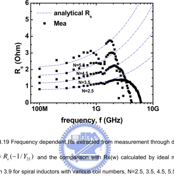
(12) Fig. 3.16. T-model for on-chip spiral inductors. (a) Equivalent circuit schematics (b) Intermediate stage of schematic block diagrams for circuit analysis. (c) Final stage of schematic block diagrams for. 47. circuit analysis.................................................................................... Fig. 3.17. T-model parameter formulas and extraction flow chart……………….. Fig. 3.18. Q(ω) calculated by equivalent circuit removing Rp from original T-model and adding Rs(w) to simulate skin effect for spiral inductors. 51. 51. with various coil numbers (a) N=2.5 (b) N=3.5 (c) N=4.5 (d) N=5.5…. Fig. 3.19. Frequency dependent Rs extracted from measurement through definition of. Rs = Re (−1/ Y21 ). and the comparison with Rs(ω). calculated by ideal model of equation 3.9 for spiral inductors with. 53. various coil numbers, N=2.5, 3.5, 4.5, 5.5……………………………... Fig. 3.20. L(ω) calculated by equivalent circuit simulation with Rp removed from original T-model for spiral inductors with various coil numbers. 53. (a) N=2.5 (b) N=3.5 (c) N=4.5 (d) N5.5………………………………… Fig. 3.21. Re(Zin(ω)) calculated by equivalent circuit simulation with Rp removed from original T-model for spiral inductors with various coil. 54. numbers (a) N=2.5 (b) N=3.5 (c) N=4.5 (d) N5.5……………………… Fig. 3.22. Q(ω) calculated by equivalent circuit simulation with Rp removed from original T-model for spiral inductors with various coil numbers. 55. (a) N=2.5 (b) N=3.5 (c) N=4.5 (d) N5.5………………………………… Fig. 3.23. Comparison of S21 (magnitude) between T-model simulation and measurement for spiral inductors. Coil numbers (a) N=1.5, (b) N=2.5, (c) N=3.5, (d) N=4.5………………………………………………. Fig. 3.24. Comparison of S21 (magnitude) between T-model simulation and. xi. 56.
(13) measurement for spiral inductors. Width for N=1.5 (a) W=3μm, (b). 56. W=9μm, (c) W=15μm, (d) W=30μm……………………………………. Fig. 3.25. Comparison of S21 (phase) between T-model simulation and measurement for spiral inductors. Coil numbers (a) N=1.5, (b). 57. N=2.5, (c) N=3.5, (d) N=4.5……………………………………………… Fig. 3.26. Comparison of S21 (phase) between T-model simulation and measurement for spiral inductors. Width for N=1.5 (a) W=3μm, (b). 58. W=9μm, (c) W=15μm, (d) W=30μm……………………………………. Fig. 3.27. Comparison of S11 (magnitude) between T-model simulation and measurement for spiral inductors. Coil numbers (a) N=1.5, (b). 59. N=2.5, (c) N=3.5, (d) N=4.5……………………………………………… Fig. 3.28. Comparison of S11 (magnitude) between T-model simulation and measurement for spiral inductors. Width for N=1.5 (a) W=3μm, (b). 59. W=9μm, (c) W=15μm, (d) W=30μm……………………………………. Fig. 3.29. Comparison of S11 (phase) between T-model simulation and measurement for spiral inductors. Coil numbers (a) N=1.5, (b). 60. N=2.5, (c) N=3.5, (d) N=4.5……………………………………………… Fig. 3.30. Comparison of S11 (phase) between T-model simulation and measurement for spiral inductors. Width for N=1.5 (a) W=3μm, (b). 61. W=9μm, (c) W=15μm, (d) W=30μm……………………………………. Fig. 3.31. Comparison of L(ω) between T-model simulation and measurement for spiral inductors. Coil numbers (a) N=1.5, (b) N=2.5, (c) N=3.5, (d). 62. N=4.5…………………………………………………………………….... Fig. 3.32. Comparison of L(ω) between T-model simulation and measurement for spiral inductors. Width for N=1.5 (a) W=3μm, (b) W=9μm, (c). xi i. 63.
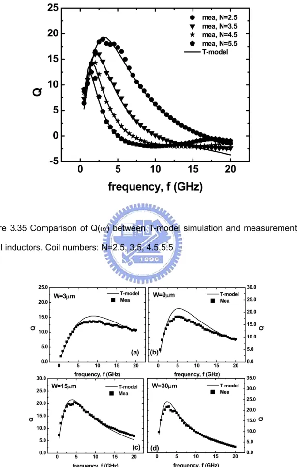
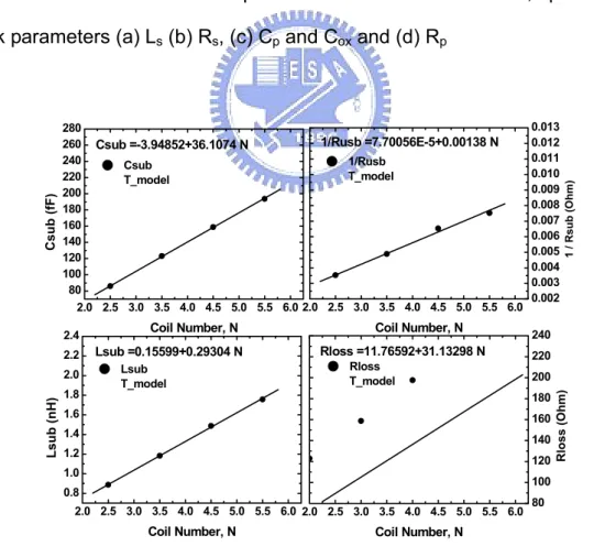
(14) W=15μm, (d) W=30μm…………………………………………………... Fig. 3.33. Comparison. of. Re(Zin(ω)). between. T-model. simulation. and. measurement for spiral inductors. Coil numbers (a) N=1.5, (b). 63. N=2.5, (c) N=3.5, (d) N=4.5……………………………………………… Fig. 3.34. Comparison. of. Re(Zin(ω)). between. T-model. simulation. and. measurement for spiral inductors. Width for N=1.5 (a) W=3μm, (b). 64. W=9μm, (c) W=15μm, (d) W=30μm……………………………………. Fig. 3.35. Comparison of Q(ω) between T-model simulation and measurement 65 for spiral inductors. Coil numbers: N=2.5, 3.5, 4.5, 5.5………………... Fig. 3.36. Comparison of Q(ω) between T-model simulation and measurement for spiral inductors. Width for N=1.5 (a) W=3μm, (b) W=9μm, (c). 65. W=15μm, (d) W=30μm…………………………………………………... Fig. 3.37. Comparison. of. Q(ω). and. self-resonance. frequency. fSR. corresponding to Q=0 among T-model, reduced T-model (Lsub = Rloss. 66. =0) and measurement for spiral inductors with various coil numbers. Fig. 3.38. (a) Self-resonance frequency fSR of on –chip spiral inductors with various coil numbers, N=2.5, 3.5, 4.5, 5.5 (a) comparison between measurement, ADS simulation, and analytical model. (b) Cp, Cox, and Csub effect on fSR calculated by ADS simulation and analytical model. Comparison with measured fSR to indicate the fSR increase. 68. contributed by eliminating the parasitic capacitances, Cp, Cox, and Csub respectively………………………………………………………….. Fig. 3.39. T-model RLC network parameters versus coil numbers, spiral coil’s 71 RLC network parameters (a) Ls (b) Rs, (c) Cp and Cox and (d) Rp……….. Fig. 3.40. T-model RLC network parameters versus coil numbers, lossy. xii i.
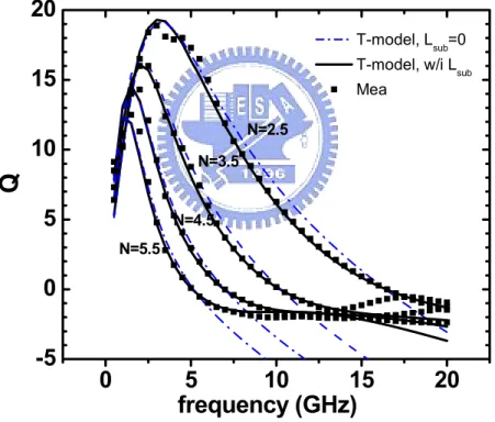
(15) substrate RLC network parameters (a) Csub (b) 1/Rsub, (c) Lsub and. 71. (d) Rloss…………………………………………………………………….. Fig. 3.41. T-model RLC network parameters versus width, spiral coil’s RLC 72 network parameters (a) Ls (b) Rs, (c) Cp and (d) Rp……………………. Fig. 3.42. T-model RLC network parameters versus wdith, lo spiral coil’s RLC 72 network parameters (a) Cox1 (b) Cox2……………………………………. Fig. 3.43. T-model RLC network parameters versus wdith, lossy substrate 73 RLC network parameters (a) Csub (b) 1/Rsub, (c) Lsub and (d) Rloss…... Fig. 3.44. Magnetic field in the single-end spiral inductor……………………….... Fig. 3.45. Improved T-model (a) equivalent circuit schematics, (b) and (c). 74. 76 schematic block diagram for circuit analysis…………………………... Fig. 3.46. Improved T-model parameter formulas and extraction flow chart……. Fig. 3.47. Comparison between ADS momentum simulation, measurement, and improved T-model for on-chip inductor (a) S11 (mag, phase) (b). 78. 80. S21 (mag, phase) (c) L(ω), Re(Zin(ω)) (d) Q(ω)…………………………. Fig. 3.48. (a) Qm (b) fm (c) fLmax (d) fSR under varying ρsi (0.01 ~ 1K Ω −cm) 81 predicted by ADS Momentum simulation……………………………….. Fig. 3.49. Improved T-model parameters under varying ρsi (a) Rsub, Rp (b) Lsub, 83 Lsub1,2, Rloss, Rloss1,2 (c) Cp (d) Cox1,2 Csub……………………………….. Fig. 3.50. Qm vs. Improved T-model parameters under varying ρsi (a) Rp (b) 83 Rsub, (c) Lsub, Lsub1,2 (d) Rloss, Rloss1,2……………………………………. Fig. 3.51. fSR vs. Improved T-model parameters under varying ρsi (a) Cp (b) 84 Csub, (c) Cox1 (d) Cox2………………………………………………………. Fig. 3.52. Comparison of improved T-model and measured S11, S21 (mag, phase) for inductors. Coil numbers (a) N=2.5 (b) N=3.5 (c) N=4.5 (d). xiii i. 85.
(16) N5.5………………………………………………………………………... Fig. 3.53. Comparison of improved T-model and measured L(ω), Re(Zin(ω)) for 86 inductors. Coil numbers (a) N=2.5 (b) N=3.5 (c) N=4.5 (d) N=5.5….... Fig. 3.54. Improved T-model parameters vs. coil number (a) Ls, Cp, Cox1,2 (b) 87 Rs, Rp (c) Csub, Lsub, Lsub1,2 (d) 1/Rsub, Rloss, Rloss1,2…………………….. Fig. 3.55. Improved T-model parameters vs. coil number (a) Ls, Cp, Cox1,2 (b) 88 Rs, Rp (c) Csub, Lsub, Lsub1,2 (d) 1/Rsub, Rloss, Rloss1,2…………………….. Chapter 4 page Fig. 4.1. Top view of a conventional differential inductor........................................ 90. Fig. 4.2. Top view of a fully symmetrical inductor…..………………….................. 91. Fig. 4.3. Qmax and fmax vs. Lmax calculated by ADS momentum for taper inductor optimization design……………………………………………... Fig. 4.4. Fully taper symmetry inductor layout………………………..................... Fig. 4.5. 2T model for fully taper symmetric inductor (a) equivalent circuit. 93 94. schematics (b) intermediate stage (c) final stage of block diagram for circuit analysis…………………………………………………………….. Fig. 4.6. 99. 2T-model parameter derivation formulas and extraction flow chart………………………………………………………………………... 99. . Fig. 4.7. Comparison of 2T-model and measurement for R=30, 60, 90 μm (a) Mag (S11) (b) Phase (S11) (c) Mag (S21) (d) Phase (S21)………………. Fig. 4.8. 104. Comparison of 2T-model and measurement under single-ended excitation for R=30, 60, 90μm (a) L (ω) (b) Re(Zin(ω))…………………. xiv i. 104.
(17) Fig. 4.9. Comparison of 2T-model and measurement under differential excitation for R=30, 60, 90μm (a) Re (Sd) (b) Im (Sd) (c) Ld (ω) (d) Re(Zd(ω))………………………………………………………………….... Fig. 4.10. Comparison of 2T-model and measurement for R=30, 60, 90 m (a) Re(Zdut1(ω)) (b) Im (Zdut1(ω)) (c) Re(Zdut2(ω)) (d) Im (Zdut2(ω))………….... Fig. 4.11. 105. Comparison. of. Q(ω). between. 2T-model. simulation. 105. and. measurement for fully taper symmetry inductor with various radiuses: R=30, 60, 90 μm………………………………………………. Fig. 4.12. 106. 2T-model RLC network parameters versus inner radius, fully taper symmetry coil’s RLC network parameters (a) Ls1,2 (b) Rs1,2 (c) Cp1,2 (d) Cox1,2,3…………………………………………………………………... Fig. 4.13. 107. 2T-model RLC network parameters versus inner radius, fully taper symmetry coil’s RLC network parameters (a) Lsk1,2 (b) Rsk1,2 (c) Rp1,2………………………………………………………………………… 108. Fig. 4.14. 2T-model RLC network parameters versus inner radius, lossy substrate RLC network parameters (a) Csub (b) 1/Rsub (c) Lsub (d) Rloss…………………………………………………………………………. xv i. 108.
(18) Chapter 1 Introduction. 1.1 Research Motivation Wireless communication has been one of major driving force for accelerated semiconductor technology progress in the current electronic industry. High frequency IC product developed for the demand of mobile communication, wireless data/voice transmission is an even more important application for global semiconductor manufacturers. Moreover, it fueled larger demand for low cost, high competitive, portable products for current market. Monolithic inductors have been commonly used in radio frequency integrated circuits (RFICs) for wireless communication systems such as wireless local area networks, personal handsets, and global position systems. The inductor is a critical device for RF circuits such as voltage-controlled oscillators (VCO), Impedance matching networks and RF amplifiers. Its characteristics generally crucially affect the overall circuit performance. However, to meet the increasingly stringent requirements driven by advancement of wireless communication systems, the characteristic of conventional monolithic inductive components is too poor to be used. In order to conform market requirement and achieve system-on-a chip (SoC), the CMOS, BiCMOS, and SiGe technologies are inevitable and passive components must be integrated. Even though SiGe or BiCMOS technologies may offer better performance, lower power, and lower noise, the much higher process complexity and fabrication cost limit their applications in consumer and communication products, which are very. 1.
(19) cost sensitive. Therefore, we focus our research on CMOS due to its higher integration and lower cost.. Besides, the circuit designers generally have critical concern about the accuracy of simulation models for active and passive components. As a result, an accurate RF device model suitable for various manufacturing technologies is strongly demanded. The mentioned requirement triggers our motivation of this work to build an accurate and scalable model for on-chip spiral inductors in RF circuit applications. Besides the accuracy and scalability, a reliable de-embedding method and an efficient model parameter extraction flow are the primary goals of this work. The accurate extraction of intrinsic device characteristics is prerequisite to accurate modeling while the challenges become tougher for miniaturized devices. An efficient model parameter extraction flow can be automated through commercial extraction tool to expedite the model extraction and optimization.. 1.2 Thesis Organization The theme of this thesis is the development of an accurate and scalable on-chip inductor model applicable for RF circuit simulation and design over broadband up to 20 GHz and beyond. In Chapter 2, I will discuss the existing issues for current inductor models, e.g. π-model.. Also, I will introduce briefly the application of pi-model which. is used to build in passive model. In Chapter 3 and Chapter 4, I will focus on the development of a broadband and scalable model for on-chip Inductor. Both single-end and symmetric inductors have been covered in this work. A new symmetric inductor of fully symmetric layout as well as taper metal line have been fabricated and a new de-embedding method has been. 2.
(20) derived to realize accurate extraction of the intrinsic device parameters. A parameter extraction flow has been established through equivalent circuit analysis to enable automatic parameter extraction and optimization. The equivalent circuit, physics phenomenon that is observation from 3D EM simulation, and analysis of extracted parameters will all be explained in these chapters. According to above concepts, we will design new model to present different inductor at the high frequency characteristics. We also improve asymmetrystructures for spiral and conventional symmetry inductor between the S11 and S22. But it can decrease the quality factor (Q) and self-resonant frequency (fSR). So we will design taper inductor to increase quality factor. For the above reason, how to improve the characteristics of passive devices and achieve low cost and high competition simultaneously is worth trying. In Chapter5, the lump-element equivalent circuit verified and analyzed by ADS circuit simulator is to simulate circuit level for different inductor modification. Chapter7 is discussed the future work and Appendixes related to analytical formula for lump-element equivalent circuit. Our analysis and inference will be verified through ADS simulation result for equivalent circuit. And we gives the conclusions to this work and its development in the future.. 3.
(21) Chapter 2 Review on Existing Inductor Models – Remaining Issues. 2.1 Requirements for inductor models for RF circuit simulation The rapid growth of the wireless communication market has fueled a large demand for low cost, high competitive, portable products. Traditionally, radio systems are implemented on the board level incorporating a lot of discrete components. Recently, compared with discrete and hybrid designs, the monolithic approach offers improved reliability , lower cost and smaller size, broadband performance, and design flexibility. In conventional design, bonding wires having a relatively high Q were used to replace on-chip inductors. However, the bonding wires generally suffer worse variations in inductance value because that they cannot be as tightly controlled as the on-chip inductors implemented by integrated circuit process. Recent advancement in silicon based RF CMOS technology can provide RF passive components such as inductors with fair performance suitable for analog and RF IC design up to several giga-hertz, then it can be integrated on a chip to match market demands. Therefore, an accurate on-chip RF passive device model applicable for circuit simulation and design becomes indispensable and the mentioned requirement triggers our motivation of this work. Extensive research work has been done to investigate inductors of various layouts and topologies such as spiral inductor, conventional symmetric inductor, and fully. 4.
(22) symmetric inductors of single-end and differential configuration. All the mentioned inductors have been fabricated on semi-conducting Si substrate for measurement, characterization as well as model parameter extraction for circuit simulation model development. In this chapter, we will introduce existing inductor models targeted for Si based RF circuit simulation. Comparison will be done for various models in terms of accuracy and bandwidth of validity, scalability and geometry of validity as well as model parameter extraction methodologies, etc.. 2.2 Analysis and comparison of existing models. Monolithic inductors have drawn increasing interest for applications in radio frequency integrated circuit (RF ICs), such as low noise amplifier (LNA), voltage controlled oscillator (VCO), Mixer , input and output match network. It is believed that SoC approach can provide benefit of lower cost, higher integration, and better system performance. However, some inherent limitations originated from the low resistivity substrate of bulk Si should be overcomed through effort in process technology and layout or new configurations in circuit operation, e.g. differenentially driven instead of single end operation. To facilitate the RF circuit simulation accuracy and prediction capability, the physical limitation coming from substrate loss, conductor loss, and the mutual interaction should be carefully considered and implemented in the circuit level models. The physical mechanisms, which are well recognized for on Si chip inductors include eddy currents on spiral metal coils and semiconducting substrate due to instantaneous electromagnetic field coupling, crossover capacitance between the spiral coils and under-pass, coupling capacitance between monolithic inductor and substrate, substrate capacitance and substrate ohmic loss, etc. In the following, the. 5.
(23) discussion on mentioned model features will be provided.. 2.2.1 Accuracy and bandwidth of validity. The lack of accurate model for on-chip inductors presents one of the most challenging problems for silicon-based RF IC design. In conventional IC technologies, inductors are not considered as standard components like transistors, resistors, or capacitors, whose equivalent circuit models are usually included in the Spice model for circuit simulation. However, this situation is rapidly changing as the demand for RF IC’s continues to grow. Various approaches for modeling inductors on silicon have been reported in past decade. Most of these models are based on numerical techniques, curve fitting or empirical formulae and therefore are relatively inaccurate for higher frequencies. For monolithic inductor design and optimization, a compact physical model is required. The difficulty of physical modeling stems from the complexity of high frequency phenomena such as the eddy currents in the coil conductor and semiconducting substrate as well as the substrate loss in the silicon. The key to accurate physical modeling is firstly to identify all the parasitic and loss effects and then to implement a physics based model for simulating the identified parasitic and loss effects. Since an inductor is intended for storing magnetic energy, the inevitable resistance and capacitance in a real inductor are counter-productive and thus are considered parasitic effects. The parasitic resistances dissipate energy through ohmic loss while the parasitic capacitances store electric energy. A traditional equivalent circuit model of an inductor generally called π-model is shown in Fig. 2.1. 6.
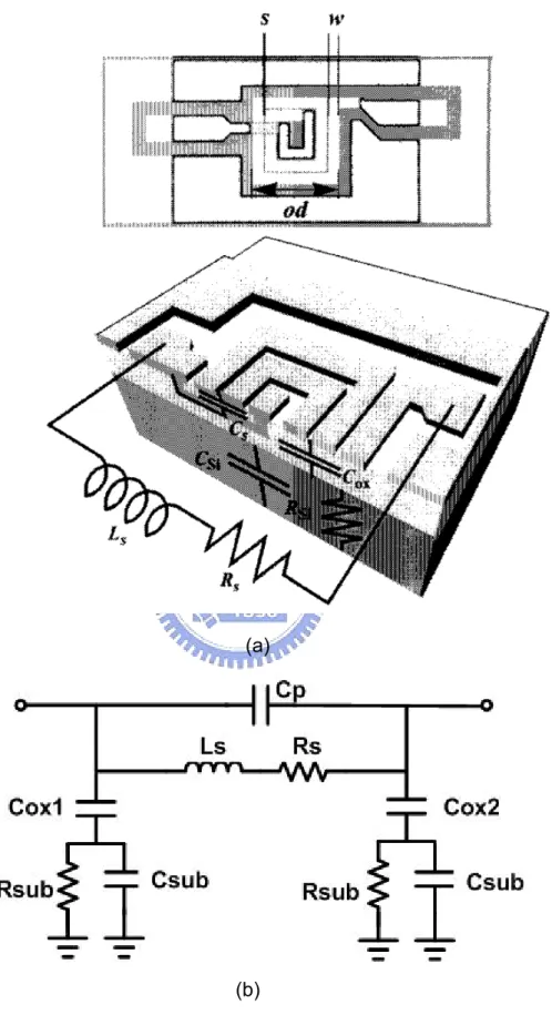
(24) (a). (b). Figure 2.1 (a) Top (die photo);Middle, 3-D view (b)the lumped physical model of a spiral inductor on silicon. 7.
(25) The inductance and resistance of the spiral and underpass is represented by the series inductance, Ls, and the series resistance, Rs, respectively. The overlap between the spiral and the underpass allows direct capacitive coupling between the two terminals of the inductor. The feed-through path is modeled by the parallel capacitance, Cp. The oxide capacitance between the spiral and the silicon substrate is modeled by Cox. The silicon substrate capacitance and resistance are modeled by Csi and Rsi. There are several sources of loss in a monolithic inductor. One relatively obvious loss comes from the series winding resistance. This is because the interconnect metal used in most CMOS processes. The DC resistance of the inductor is easily calculated as the product of this sheet resistance and the number of squares in the metal strip. However, at high frequencies the resistance of the strip increases due to skin effect, proximity effect and current crowding. The substrate loss will increase with frequency due to the dissipative currents that flow in the silicon substrate. In fact, there are two different physical mechanisms that cause the induction of these currents and opposition flux.. Although physical considerations are included in such a structure, the original π-model lacks the following import feature: 1. Strong frequency dependence of series inductance and résistance as a result of the current crowding in the crowding 2. Frequency-independent circuit structure that is compatible with transient analysis and broadband design 3. It is difficulty to match high frequency behaviors, especially for thick metal case where metal-line-coupling capacitance is not negligible and substrate loss.. According to above theory and original π-model, we modify π-model for on-chip spiral. 8.
(26) inductors over again to fit measurement data. Moreover, we add two new element Rp and Lsub to improve above third item, as shown figure 2.2. A parallel Rp is to simulate current crowding in coil’s RLC network and series Lsub1,2 are placed under the Cox1,2 to be represent eddy effect in the substrate RLC network. In order to verify the accuracy of the modify π-model, spiral inductors with various geometrical configurations were fabricated using 0.13 μm eight-metal CMOS technology. To assess the model validity, we compare difference with model and measurement.. Figure 2.2 Modify π-model for on-chip spiral inductors.. Figure 2.3 and 2.4 show the measured and modeled S-parameters, mag(S21) and phase(S21) for a varying coil number of turns. As can be seen from these figures, the S-parameters of model match the measured data worst, especially a lager turn (N=3.5, 4.5, 5.5) at the high frequency. Figure 2.5 (a) ~ (d) reveal the exact match of Mag(S11). 9.
(27) for smaller coils (N= 2.5, 3.5) over full frequency range up to 20GHz, but the other figure 2.6 shows enormous error of phase(S11). Due to above match condition, modify π-model may be not suit to simulate measured S-parameters for spiral inductors. Besides, we also make comparison with performance parameters for spiral inductor, i.e., L(ω), Re(Zin(ω)), and Q(ω). From figure 2.7 ~ 2.9 illustrates, we find that the modify π-model provides very good match with the measurement for L(ω), Re(Zin(ω)), and Q(ω) before self-resonance frequency. According to above comparison, modify π-model may be not simulate all parameters of spiral inductors and maybe can simulate certain specific parameters, especially L(ω), Re(Zin(ω)), and Q(ω). Hence, in the following chapter, we will change equivalent circuit structure over again. We use 3D EM simulation by Ansoft HFSS to simulate on-chip inductor and discover truly conforms to the physics significance parameter to establish new equivalent circuit.. -5. -10. -10. -15. -15. -20. -20. -25. -25. -30 -40 0. 2. 4. 6. 8 10 12 14 16 18 20 0. 2. 4. frequency, f (GHz) 0. 6. -35. 8 10 12 14 16 18 20. -40. frequency, f (GHz) π_model_5.5 mea_5.5. (c). -5. -30. π_model_3.5 mea_3.5. π_model_2.5 mea_2.5. -35. Mag (S21). 0. (d). 0 -5. -10. -10. -15. -15. -20. -20. -25. -25. -30 -40 0. -30. π_model_4.5 mea_4.5. -35 2. 4. 6. Mag (S21). Mag (S21). (b). (a). Mag (S21). 0 -5. -35. 8 10 12 14 16 18 20 0. frequency, f (GHz). 2. 4. 6. 8 10 12 14 16 18 20. -40. frequency, f (GHz). Figure 2.3 Comparison of S21 (magnitude) between π-model simulation and measurement for spiral inductors. Coil numbers (a) N=1.5, (b) N=2.5, (c) N=3.5, (d). 10.
(28) N=4.5. 0. (b). (a). 50. -60. 0. -80. -50. -100 π_model_2.5 mea_2.5. -120 0. 2. 4. 6. -100. π_model_3.5 mea_3.5. 8 10 12 14 16 18 20. 0. 2. 4. frequency, f (GHz) 200. 6. -150. 8 10 12 14 16 18 20. frequency, f (GHz). 200. (d). (c). 150. 50. 50. 0. 0. -50. -50. -100. -100. π_model_5.5 -150 mea_5.5 -200. π_model_4.5 mea_4.5. -150 -200 0. 150 100. 100. phase (S21). phase (S21). 100. -40. -140. 150. 2. 4. 6. phase (S21). phase (S21). -20. 200. 8 10 12 14 16 18 20 0. 2. 4. 6. 8 10 12 14 16 18 20. frequency, f(GHz). frequency, f (GHz). Figure 2.4 Comparison of S21 (phase) between π-model simulation and measurement for spiral inductors. Coil numbers (a) N=1.5, (b) N=2.5, (c) N=3.5, (d) N=4.5. -5. -5. -10. -10. -15. -15. -20. -20. -30 0. π_model_3.5 mea_3.5. π_model_2.5. -25. mea_2.5 2. 4. 6. 8 10 12 14 16 18 20 0. 2. 4. frequency, f (GHz) 0. 6. 8 10 12 14 16 18 20. frequency, f (GHz). (d). (c). Mag (S11). -25 -30 0 -2 -4. -5. -6 -10. -8 -10. -15 -20 0. Mag (S11). 0. (b). (a). π_model_4.5 mea_4.5. 2. 4. 6. 8 10 12 14 16 18 20 0. frequency, f (GHz). π_model_5.5 mea_5.5. 2. 4. 6. Mag (S11). Mag (S11). 0. -12 -14. 8 10 12 14 16 18 20. frequency, f (GHz). Figure 2.5 Comparison of S11 (magnitude) between π-model simulation and measurement for spiral inductors. Coil numbers (a) N=2.5, (b) N=3.5, (c) N=4.5, (d). 11.
(29) N=5.5. 100. (b). (a). 20. 0. 0 -20. -50. -40. -150 0. π_model_3.5 mea_3.5. π_model_2.5 mea_2.5. 2. 4. 6. 8 10 12 14 16 18 20 0. 2. 4. frequency, f (GHz). 200. 6. -60 -80. 8 10 12 14 16 18 20. frequency, f (GHz). (c). 150. phase(S11). 40. -100. phase(S11). 60. (d). 200 150. 100. 100. 50. 50. 0. 0 -50. -50 -100. π_model_4.5 mea_4.5. -150 -200 0. 2. 4. 6. -100. π_model_5.5 mea_5.5. 8 10 12 14 16 18 20 0. 2. 4. frequency, f (GHz). 6. phase(S11). phase(S11). 50. 80. -150. 8 10 12 14 16 18 20. -200. frequency, f (GHz). Figure 2.6 Comparison of S11 (phase) between π-model simulation and measurement for spiral inductors. Coil numbers (a) N=2.5, (b) N=3.5, (c) N=4.5, (d) N=5.5. 10.0n π_model_3.5 8.0n mea_3.5 6.0n. (b). π_model_2.5 mea_2.5. 4.0n. 4.0n. 2.0n. 2.0n 0.0. 0.0. -2.0n. -2.0n -4.0n 0. -4.0n 2. 4. L (H). 6. 8 10 12 14 16 18 20 0. 2. 4. 8 10 12 14 16 18 20. -6.0n. 20.0n π_model_5.5 15.0n mea_5.5. (d). π_model_4.5 mea_4.5. (c). 6. frequency, f (GHz). frequency, f (GHz). 20.0n 15.0n. L (H). L (H). 6.0n. (a). 10.0n. 10.0n. 5.0n. 5.0n 0.0. 0.0. -5.0n. -5.0n -10.0n 0. L (H). 8.0n. -10.0n 2. 4. 6. 8 10 12 14 16 18 20 0. frequency, f (GHz). 2. 4. 6. 8 10 12 14 16 18 20. frequency, f (GHz). Figure 2.7 Comparison of L(ω) between π-model simulation and measurement for. 12.
(30) spiral inductors. Coil numbers (a) N=2.5, (b) N=3.5, (c) N=4.5, (d) N=5.5. 400. 400. 200. 200. 0. 2. 4. 6. 8 10 12 14 16 18 20 0. 2. 4. frequence, f (GHz). 1000. π_model_4.5 mea_4.5. 800. 6. 8 10 12 14 16 18 20. Re(Zin) (Ohm). 600. 0. frequence, f (GHz). 1000 π_model_5.5 mea_5.5 800. (d). (c). 600. 600. 400. 400. 200. 200. 0. 0. 2. 4. 6. 8 10 12 14 16 18 20 0. 2. 4. 6. 8 10 12 14 16 18 20. Re(Zin) (Ohm). Re(Zin) (Ohm). π_model_3.5 800 mea_3.5. 600. 0. Re(Zin) (Ohm). (b). (a). π_model_2.5 meal_2.5. 800. 0. frequence, f (GHz). frequence, f (GHz). Figure 2.8 Comparison of Re(Zin(ω)) between π-model simulation and measurement for spiral inductors. Coil numbers (a) N=2.5, (b) N=3.5, (c) N=4.5, (d) N=5.5. mea_2.5 mea_3.5 mea_4.5 mea_5.5 π_model. 20 15. Q. 10 5 0 -5. 0. 5. 10. 15. 20. frequency, f (GHz) Figure 2.9 Comparison of Q(ω) between π-model simulation and measurement for. 13.
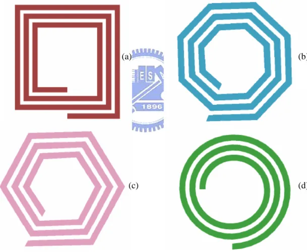
(31) spiral inductors. Coil numbers (a) N=2.5, (b) N=2.5, (c) N=3.5, (d) N=4.5. 2.2.2 Scalability and geometries of validity. There are various geometries available for a monolithic inductor to be implemented, e.g. rectangular, hexagonal, octagonal, and circular as shown in figure 2.10.. (a). (b). (c). (d). Figure 2.10 Spiral inductor geometries.. Electromagnetic (EM) simulation can help to verify the layout geometry effect on inductors and the results suggest that circular spiral can provide the best performance. 14.
(32) in terms of higher quality factor and smaller chip area.. The mechanism responsible. for the improved performance realized by circular spiral comes from the reduced current crowding effect. The circular inductor as shown in figure 2.2 (d) can place the largest amount of conductor in the smallest possible area, reducing the series resistance and parasitic capacitance of the spiral inductors. However, one major drawback of the circular structure is its layout complexity. It is because that its metal line consists of many cells rotated with different angles. In general, specific coding is required to generate this structure by layout tools. In fact, a good model is developed to accurately simulate the broadband characteristics of on-Si-chip for different geometries of the inductive passive components, up to 20GHz. Besides the broadband feature, scalability is justified by good match with a liner function of geometries of the inductive passive components for all model parameters employed in the RLC network. The satisfactory scalability manifest themselves physical parameters rather than curve fitting.. 2.2.3 Model parameter extraction flow and automation. Which a new model or a conventional model has been developed to accurately simulate the broadband characteristics, its all the unknown R, L,C parameters haven’t been determined initial value. So we must establish a parameter extraction flow through equivalent circuit analysis to determine initial guess value and to enable automatic parameter extraction and optimization. All the unknown R,L,C parameters are extracted from analytical equations derived from different equivalent circuit analysis. We can use Z-matrix and /or Y-matrix to extract all parameters. Above extraction and optimization principle, we use some principle to define a set of. 15.
(33) analytical equation from measurement and to generate all unknown parameters at the equivalent circuits. Due to the necessary approximation, the extracted R,L,C parameters in the first run of low are generally not the exactly correct solution but just serve as the initial guess or further optimization through best fitting to the measured S-parameters, L(ω), Re(ω), and Q(ω).. 2.3 Model enhancement strategies The lack of an accurate and scalable model for on-chip inductors becomes one of the most challenging problems for Si-based RF IC design. The existing models suffer two major drawbacks in terms of accuracy for limited bandwidth and poor scalability. Many reference publications reported improvement on the commonly adopted π-model by modification on the equivalent circuit schematics. However, limited band width to few gigahertz remains an issue for most of the modified π-models. A two π-model was proposed to improve the accuracy of R(ω) and L(ω) beyond self-resonance frequency. Unfortunately, this two π-model suffers a singular point above resonance. Besides, the complicated circuit topology with double element number will lead to difficulty in parameter extraction and greater time consumption in circuit simulation. Recent work using modified T-model demonstrated promising improvement in broadband accuracy and suggested the advantage of T-model over π-model. However, the scalability of model’s major concern was not presented. To solve the mentioned issues, a new T-model was proposed and developed in this work. This T-model is proposed to realize two primary features, i.e., broadband accuracy and scalability. The T-model is composed of two RLC networks to account for spiral coils, lossy substrate, and their mutual interaction. Four physical elements, Rs Ls Rp and Cp are incorporated to describe the spiral coils above Si substrate and other elements. All the physical elements are constants independent of frequencies and can. 16.
(34) be expressed by a close form circuit analysis on the proposed T-model. Parameter extraction and optimization can be conducted with an initial guess extracted by approximation valid for specified frequency range. All the model parameters manifest themselves with predictable scalability w.r.t. coil numbers and physical nature. A parameter extraction flow has been established to enable automatic parameter extraction and optimization that is easy to be adopted by existing circuit simulators like Agilent ADS or parameter extractor such as Agilent IC-Cap. The model accuracy over broadband is validated by good agreement with the measured S-parameters, L(W), Re(Zin(W)), and Q(W) up to 20GHz that this scalable inductor model can effectively improve RF circuit simulation accuracy in broad bandwidth and facilitate the design optimization using on-chip inductors.. 2.4 Fundamental of quality factor for an inductor. For an ideal inductor free from energy loss due to parasitic resistance and substrate coupling effect, the magnetic energy stored can be given by (2.1),. EL = Where. iL. 1 2 LiL 2. (2.1). is the instantaneous current through the inductor.. From (2.1), the peak magnetic energy stored in an inductor in sinusoidal steady state is given by, 2. E peak inductor Where. IL. and. VL. V 1 2 = L I L = L2 2 2ω L. (2.2). correspond to the peak current through and the peak voltage. across the inductor.. 17.
(35) The quality factor (Q) of an inductor is a measure of the performance of the elements defined for a sinusoidal excitation and given by,. Q = 2π. energy stored energy stored =ω energy loss per cycle average power loss. (2.3). The above definition is quite general which causes some confusion. However, in the case of an inductor, energy stored refers to the net peak magnetic energy. To illustrate the determination of Q, consider an ideal inductor in series with a resistor in Figure 2.11. This models an inductor with resistance in the winding.. Figure 2.11 Inductor with a series resistance. Since the current in both elements is equal, we use the equation for the peak magnetic energy in terms of current given in (2.2) to write,. peak magnetic energy stored energy loss per cycle 1 2 I s Ls ω L s 2 = 2π = 1 2 Rs I s Rsτ 2 where. Q = 2π. 2π. τ. =ω. Where τ is the period of the sinusoidal excitation. 18. (2.4).
(36) Note that the quality factor of an inductor with a lossy winding increases with frequency. Also note that as the resistance in the inductor decreases, the quality of the inductor increases and in the limit Q becomes infinite since there is no loss. Using the above procedure, the quality factor of another pure lossy inductor can be determined. We repeat the detail in the following.. Figure 2.12 Inductor with a parallel resistance.. Since the voltage in both elements is equal, we use the equation for the peak magnetic energy in terms of voltage given in (2.2) to write,. Q = 2π. peak magnetic energy stored energy loss per cycle 2. Vp. 2ω 2 Lp. = 2π. Vp. 2. 2ω Rp 2. =. (2.5). τ. Rp. ω Lp. Where τ is the period of the sinusoidal excitation. 19.
(37) The definition of quality factor is general in the sense that it does not specify what stores or dissipates the energy. The subtle distinction between an inductor and an LC tank Q lies in the intended form of energy storage. For example, only the magnetic energy stored is of interest and any electric energy stored because of some inevitable parasitic capacitance in a real inductor is counterproductive. Therefore, the Q of an inductor is proportional to the net magnetic energy stored and is given by,. peak magnetic energy stored energy loss per cycle peak magnetic energy stored-peak electric energy = 2π energy loss per cycle. Qinductor = 2π. (2.6). An inductor is said to be self-resonant when the peak magnetic and electric energies are equal. Therefore, Q of an inductor vanishes to zero at the self-resonant frequency. At frequencies above the self-resonant, no net magnetic energy is available from an inductor to any external circuit. In contrast, for an LC tank, the Q is defined at the resonant frequency. ωo , and the energy stored term in the wxpression. for Q given by (2.3) is the sum of the average magnetic and electric energy. Since at resonance the average magnetic and electric energies are equal, so we have,. Qinductor = 2π. average magnetic energy + average electric energy energy loss per cycle ω =ωo. peak magnetic energy = 2π energy loss per cycle. ω =ωo. peak electric energy = 2π energy loss per cycle ω =ωo. (2.7). The average magnetic or electric energy at resonance for sinusoidal excitation is. 20.
(38) 1 1 2 2 L I L = C Vc 4 4. which are half the peak magnetic energy given by (2.2) Lets. look at the parallel RLC circuit of figure 2.5 to clarify its inductor and tank Q.. Figure 2.13 Parallel RLC circuit.. The quality factor of the inductor is calculated as follows,. Qinductor = 2π. peak magnetic energy - peak electric energy energy loss per cycle. Vp. = 2π. 2. 1 − C p Vp 2 2ω Lp 2 Vp. 2. 2. 2 Rp. T. 1 − ωC p ω Lp = 1 Rp. (2.8). 2 Rp ⎧⎪ ⎛ ω ⎞ ⎫⎪ = ⎨1- ⎜ ⎟ ⎬ ω Lp ⎪ ⎝ ωo ⎠ ⎪ ⎩ ⎭. where the resonant frequency. Here. Rp. ω Lp. ω0 =. 1 Lp C p. .. accounts for the magnetic energy stored and ohmic loss of the parallel. resistance in figure 2.4. The second term in equation 2.8 is the self-resonance factor describing the reduction in Q due to the increase in the peak electric energy with. 21.
(39) frequency and the vanishing of Q at the self-resonant frequency. In the parallel RLC circuit, VL = VC = VP which is depicted in the figure 2.5. Note that in each quarter cycle, when energy is being stored in the inductor, it is being released from the capacitor and vice versa. As ω increases, the magnitude of. IC. IL. decreases while the magnitude of. increases until they become equal at the resonant-frequency ω0, so that an equal. amount of energy is being transferred back and forth between the inductor and. Qinductor given. capacitor. At this frequency, above ω0, the magnitude of. IL. by equation 2.8 is zero. As ω increases. becomes increasingly more negative. That is, as the. previous mention, no net magnetic energy is available from an inductor to any external circuit at frequency above ωo . The inductor is capacitive in nature, and. Qinductor given by (2.8) is negative. Now using (2.7) to calculate the tank Q we have. Qtan k = 2π. peak magnetic energy energy loss per cyle ω =ω. o. Vp = 2π. 2. 2ω 2 Lp Vp. =. 2. 2 Rp. T ω=. Rp Lp. =ω0 Rp C p. (2.9). Cp. 1 Lp C p. Note that the tank Q isn’t zero unlike the inductor Q which is zero at resonance. Also, note that the same result can be derived using the ratio of the resonant-frequency to -3 dB bandwidth as follows,. 22.
(40) Qtan k =. =. f BW−3dB f 1 2π Rp C p. f = fo. = f=. 1 2π L p C p. Rp Lp. ω0 Rp C p. (2.10). Cp. (2.9) and (2.10) are the same as we expect.. Both Q definitions discussed above are important, and their applications are determined by the intended function in a circuit. While evaluating the quality of on-chip inductors as a single element, the definition of inductor quality given by (2.6) is more appropriate. However, if the inductor is being used in a tank, the definition given by (2.7) is more appropriate. Figure 2.6 shows a real inductor can be replaced by a parallel RLC circuit of π-model.. Figure 2.14 Alternative method for determining the Q in real inductors. In contrast with (2.8), it can be easily determined that the real inductor quality. 23.
(41) factor of a parallel RLC circuit is given by the negative of the ratio of the imaginary part to the real part of the input admittance, namely the ratio of the imaginary part to the real part of the input impedance. The above statements are summarized in (2.11) and are appropriate for determining the Q of inductors from simulation or measurement results.. Qtan k =. Im {Zin }. Re {Zin }. =−. Im {Yin }. Re {Yin }. 24. (2.11).
(42) Chapter 3 Broadband and Scalable On-chip Inductor Model. 3.1 Broadband accuracy for on-chip inductors. In silicon-based radio-frequency (RF) integrated circuits (ICs), on chip spiral inductor are widely used due to their low cost and ease of process integration. As a necessary tool for circuit design, equivalent circuit models of spiral inductors, using lumped RLC elements, efficiently represent their electrical performance for circuit simulation with other design components. Compared with the generic 3D electromagnetic field solver (e.q., HFSS) or other 2.5D electromagnetic field solver (e.q., ADS Momentum), a lumped equivalent-circuit model dramatically reduces computation time and supports rapid performance optimization. On the other hand, model inaccuracy, which stems from the complexity of on-chip inductor structures and high-frequency phenomena, presents one of the most challenging problems for RF IC designers. Current equivalent-circuit approaches simply represent the inductor as a lumped circuit and π-model is one of examples. π-model includes series metal resistance and inductance, feedthrough capacitance, dielectric isolation, and substrate effects. A physical model is proposed to capture the high-frequency behavior as shown in Fig. 3.1.. Herein, the spiral inductor was built on Si substrate where the high-frequency. behavior is complicated due to semi-conducting substrate nature. The conventional π-model reveals limitation in broadband accuracy due to some neglected effects such as eddy current on substrate. In order to overcome this disadvantage, 3D EM. 25.
(43) simulation was done using HFSS to investigate the lossy substrate effect. Following the HFSS simulation results, a new T-model has been developed to accurately simulate the broadband characteristics of on-Si-chip spiral inductors, up to 20 GHz.. Figure 3.1 Conventional π-model. 3.1.1 Simulation tool and simulation method Some electromagnetic (EM) field simulators are used, like sonnet, microwave office, HFSS and ADS Momentum to predict the component characteristics such as S-parametera, quality factor, and self-resonant frequency. However, we found that the simulation time of HFSS for 3D is slower than the others. Because it can estimate the magnetic substrate eddy current effect, we can obtain more accurate S-parameter. ADS Momentum EM simulation is a planar full-wave EM solver that can calculate the fields in the substrate and the dielectric and spend less time, but this simulation tools for 2.5D is less accurate than HFSS. Thus, the capacitance between the spiral windings and the eddy current in the windings are not modeled. The advantage of. 26.
(44) these EM simulators is that they can report their simulation results in S-parameters. These results can then be numerically fitted to the circuit model. But in general, it is desirable to simulate circuits with these components by directly using the S-parameters extracted from the EM simulator or measured from the instruments. This is because a number of the component values in this circuit model vary with frequency due to the skin effect, substrate loss and so on. For the mentioned reason, the fast and adequately accurate simulation program is strongly demanded. In order to predict the frequencies corresponding to Qmax and self-resonance (fSR), the amount of the parasitic capacitance should be predicted accurately. Due to the requirement, we select HFSS for EM simulation and analysis in this work.. Figure 3.2 layer stackup simulation by HFSS. 27.
(45) Spiral inductors were fabricated by 0.13um back end technology with eight layers of Cu and low-k inter-metal dielectric (k=3.0). The top metal of 3μm Cu was used to implement the spiral coils of width fixed at 15μm and inter-coil space at 2μm. The inner radius is 60μm and outer radius is determined by different coil numbers N=2.5, 3.5, 4.5, 5.5 for this topic. The physical inductance achieved at sufficiently low frequency are around 1.96~8.66nH corresponding to coil numbers N=2.5~5.5. S-parameters were measured by using Agilent network analyzer up to 20 GHz and de-embedding was carefully done to extract the truly intrinsic characteristics for model parameter extraction and scalable model build up. In Figure 3.2, it is clear that HFSS simulation environment is a solid structure. In HFSS simulation window, it can’t simulate 0.13um back end technology with eight layers of Cu and low-k inter-metal dielectric (k=3.0), so we must make some modifications for simulation setup.. Figure 3.3 effective oxide dielectric constant equivalents from M1 to M2. From Figure 3.3, we give an example for dielectric constant equivalent from Metal-1 to Metal-2. In 0.13um back end technology, the inter-metal dielectrics is a complex layer structure of various dielectric constants. In order to simplify these layers, we make two. 28.
(46) series capacitances be equal to one capacitance. We use above theory to extend complex type and show the formula as follows n. Deff = ∑ di. (3.1). i =1. ε r ,eff. ⎛ n di ⎞ = Deff × ⎜ ∑ ⎟ ⎝ i =1 ε ri ⎠. −1. (3.2). Where εr is relative permittivity and di is thickness. In the layout of the inductor, to prevent flux radiation to cause flux degradation in the center area, we generally plot ground ring to protect flux radiation. As shown in Fig 3.4, in order to simulate ground ring by HFSS, we could setup ground ring material for PEC to decrease the loss. Adopting the described simulation method, we will discuss T-model build-up for single-end spiral inductor in the next section.. Figure 3.4 Ground ring setup by HFSS. 29.
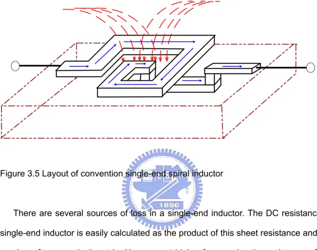
(47) 3.1.2 Conductor and substrate loss effect – model and theory. Figure 3.5 Layout of convention single-end spiral inductor. There are several sources of loss in a single-end inductor. The DC resistance of single-end inductor is easily calculated as the product of this sheet resistance and the number of squares in the strip. However, at higher frequencies the resistance of the strip increases due to the skin effect and current crowding. Moreover, substrate losses increase with frequency due to the dissipative currents that flow in the silicon substrate. According to Maxwell equation, there are tow different mechanisms that cause the induction of these loss effects. One is the capacitive coupling between the strip and the substrate induces display current, namely electric substrate losses. The other is the magnetic is the magnetic coupling caused by the time varying magnetic field linked to the strip induces eddy currents under the strip and in the inner turns of the strip, namely magnetic substrate losses. From (3.3) and (3.4) of Maxwell equation, we can show above theory.. 30.
(48) G G ∂B ∇× E = − ∂t. (3.3). G G G G ∂ ∇ × E • dS = − B • dS ∫∫ ∂t ∫∫ G G ∂Φ A E • d = − v∫ c ∂t. (3.4). Figure 3.5 show the electric and magnetic substrate losses of single-end spiral inductor. The magnetic field. JJJJG B(t ). extends around the windings and into the. substrate. Faraday’s Law states that this time-varying magnetic field will induce an electric field in the substrate. This field will force an image current to flow in the substrate in opposite direction of the current in the winding directly above it. The magnetic field will not only penetrate into the substrate but also into the other windings of the coil. The effect causes the inner turns of the strip to contribute much more loss to the inductor while having a minimal impact on the actual inductance. This phenomenon is sometimes referred to as current crowding. For on-chip single-end spiral inductors, the line segments can be treated as microstrip transmission lines. In this case, the high frequency current recedes to the bottom surface of the wire, which is above the ground plane. Please see figure 3.6.. Figure 3.6 cross section for single-end spiral inductor coils. 31.
(49) 2. The attenuation of the current density ( J in A / m ) as a function of distance (y) away from the bottom surface can be represented by the function. J = Jo × e. −. y. δ. (3.5). The skin depth ( δ ) shows below equation 3.6. 2. δ=. The current ( I in A) is obtained by integrating Since. J. (3.6). ωμσ. I. only varies in the y direction,. J. over the wire cross-sectional area.. can be calculated as. G G i = ∫ J • dS s. d. −. y. = ∫ J o × e × w • dy δ. (3.7). 0. −. d. = J o wδ (1 − e δ ) Where. d. is the physical thickness of the wire. The last term in equation 3.6 can be. defined as an effective thickness −. d. deff = δ (1 − e ) δ. (3.8). The dc series resistance, Rdc, can be expressed as. RDC = Rsh. l w. (3.9). The series resistance, Rs, can be expressed as. Rs =. l −. (3.10). d. σ wδ (1 − e ) δ. We can use Taylor’s expansion, so we can obtain frequencies.. Rs = RDC. at the low. At the higher frequencies, we will include skin effect depended on. 32.
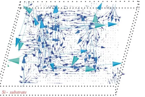
(50) frequency in the (3.10). Regarding to substrate effect, we use 3D simulation tools, for example, HFSS to simulate current flow direction on the substrate surface to verify above theory. The simulated current flow expressed by vectors is shown in figure 3.7. Figure 3.7 simulate eddy current on the substrate surface by HFSS. Figure 3.7 indicates that the eddy current on the Si substrate flows in the opposite direction w.r.t that of spiral coils. According to Faraday’s Law states that this time-varying magnetic field will induce an electric field in the substrate and generate a current on the substrate surface. But in the interior substrate also is generated, we also obtain result from 3D simulation tools by HFSS. From figure 3.8, we find current generated in the interior substrate. This effect also causes Q degeneration of the single-end spiral inductors. In order to decrease magnetic field coupling to substrate, we usually use pattern ground shield at the lower metal and increase Q value.. 33.
(51) Figure 3.8 simulate eddy current in the interior substrate surface by HFSS. According to above method, we will present a new T-model developed to accurately simulate the broadband characteristics of single-end spiral inductors. In figure 3.9, we integrate all physic parameters and obtain a compact model. Please see figure 3.9, and we will use equivalent circuit to analysis in the next section.. 34.
數據
+7

相關文件
Step 3: : : :模擬環境設定 模擬環境設定 模擬環境設定 模擬環境設定、 、 、 、存檔與執行模擬 存檔與執行模擬
Finally, we use the jump parameters calibrated to the iTraxx market quotes on April 2, 2008 to compare the results of model spreads generated by the analytical method with
The objective of the present paper is to develop a simulation model that effectively predicts the dynamic behaviors of a wind hydrogen system that comprises subsystems
It is concluded that the proposed computer aided text mining method for patent function model analysis is able improve the efficiency and consistency of the result with
This study integrates consumption emotions into the American Customer Satisfaction Index (ACSI) model to propose a hotel customer satisfaction index (H-CSI) model that can be
Meanwhile, the customer satisfaction index (SII and DDI) that were developed by Kuo (2004) are used to provide enterprises with valuable information for making decisions regarding
IPA’s hypothesis conditions had a conflict with Kano’s two-dimension quality theory; in this regard, the main purpose of this study is propose an analysis model that can
在軟體的使用方面,使用 Simulink 來進行。Simulink 是一種分析與模擬動態
