行政院國家科學委員會專題研究計畫 成果報告
後次微米時代新興電子設計自動化技術之研究--子計畫
三:角落錯誤之矽除錯(3/3)
研究成果報告(完整版)
計 畫 類 別 : 整合型 計 畫 編 號 : NSC 99-2220-E-009-010- 執 行 期 間 : 99 年 08 月 01 日至 100 年 07 月 31 日 執 行 單 位 : 國立交通大學電子工程學系及電子研究所 計 畫 主 持 人 : 周景揚 共 同 主 持 人 : 趙家佐 計畫參與人員: 碩士班研究生-兼任助理人員:石銘恩 碩士班研究生-兼任助理人員:張玟翔 碩士班研究生-兼任助理人員:徐浩文 碩士班研究生-兼任助理人員:黃欽遠 博士班研究生-兼任助理人員:雷永群 博士班研究生-兼任助理人員:潘&;#30026;宇 博士班研究生-兼任助理人員:楊皓宇 博士班研究生-兼任助理人員:穆思邦 博士班研究生-兼任助理人員:黃雅詩 公 開 資 訊 : 本計畫可公開查詢中 華 民 國 100 年 10 月 31 日
中文摘要: 由於越來越高的晶片複雜度、製程的不穩定性以及先進製成技 術的不完整特徵曲線,在今日的晶片設計中第一次製作的晶片 經常都是失敗或是因為太低的良率而無法被接受。根據從失敗 的晶片中蒐集錯誤的訊息,錯誤分析被使用以找出錯誤的原因 所在,稍後可被使用以更正設計、改進製成或是增進下次量產 晶片時的良率。但是,由於今日設計以及製程複雜度不停地增 加,使得錯誤分析越來越困難並且需要更多的時間來達成。因 此,時間、成本以及錯誤分析的效率很明顯地影響晶片設計的 時程以及成本。 在這個子計畫中,我們對於多重 stuck-at 錯誤提出了一個錯誤 診斷架構。這個架構包括了兩個主要部分:錯誤區域辨識以及 錯誤候選邏輯閘排序。在錯誤區域辨識中,我們使用了錯誤以 及通過的測試向量,並使用 X 模擬技術以及位元翻轉技術藉以 迅速的縮小包括了所有錯誤的區域。與其他區域基礎的方法不 同,我們的架構並不需要對於錯誤區域做出半徑假設,因此是 更具有彈性的。在錯誤候選邏輯閘排序中,我們辨認以及排序 這些錯誤候選邏輯閘根據之前錯誤區域辨認時所蒐集之資訊。 實驗數據說明了我們提出的診斷架構,在即使 SLAT 測試向量 的數目以及錯誤向量所佔的百分比率都很低的情況之下,仍然 可以有效率並迅速地縮小錯誤區域並且從錯誤區域中找出真實 的錯誤位置。這部分對於傳統的以 SLAT 為基礎或是區域基礎 的方法仍然是非常困難的部分。 本子計畫的另一部分是要定一設計在矽除錯時的可偵錯度,並 利用可見度計畫來選取在矽除錯中可被觀察之訊號,以最大化 此設計之可偵錯度。在錯誤分析中,給定錯誤模型之下,一種 被稱為錯誤診斷的技術被使用於找出可能的錯誤候選邏輯閘。 藉由這些回報出的錯誤候選邏輯閘,晶片設計師可以較容易藉 由聚焦離子束 focused-ion-beam (FIB)技術找到可能錯誤的實際 位置。這些物理直接檢查的技術在目前的工業界中仍是非常的 緩慢以及昂貴。因此,一種具有高精準度以及高效率的錯誤診 斷架構是非常迫切的需求用以加速以及降低錯誤診斷整個過程 的時間與成本。然而由於製程的演進,在偵錯的過程中,僅有 非常少的訊號能夠藉由 FIB 技術被觀察到。因此我們提出一個 偵錯導向的設計架構,對於完成擺放及繞線的版圖進行調整, 使得在偵錯階段有更多的訊號能夠被 FIB 技術觀察甚至修正。 在 90 奈米的製程下,實驗證明我們提出的方法能夠有效地提升 訊號被 FIB 技術觀測及修正的比率。此外,整體電路的面積及 速度幾乎不受影響。
英文摘要: Due to the high complexity, high variation, and incomplete
silicons of today’s ICs usually fail or suffer an unacceptable low yield. Based on the collected responses of failed chips, the failure analysis is applied to identify the root causes of the failure, which are then used to correct the design, improve the process, or enhance the yield for the next silicon. However, the nonstop increase of today’s design complexity and process complexity has made the failure analysis more and more difficult and time-consuming. Therefore, the time, cost, and effectiveness of the failure analysis significantly affects IC’s time-to-market and total cost.
In this project, we propose a diagnosis framework targeting multiple stuck-at faults. This framework consists of two main components, the faulty-region identification followed by the fault-candidate ranking. In the faulty-region identification, we utilize the X-simulation technique and the bit-flipping technique to gradually shrink the suspect region covering all real faults based on both failing and passing patterns. Unlike the region-based methods, our framework requires no assumption for the radius of the suspect region and hence is more flexible. In the fault-candidate ranking, we classify and rank the fault candidates based on the information collected from the faulty-region identification. The experimental results show that the proposed diagnosis framework can efficiently and effectively minimize the suspect region and sieve out the real faults from the region even when the failing-pattern percentage and the number of SLAT patterns are both low for the circuits under diagnosis (CUDs). Those are the difficult cases to be diagnosed by the traditional SLAT-based and region-based methods.
Another part of this project is to define the diagnosibility for silicon debug and to maximum the diagnosibility of designs by the signals which are selected from visibility planning. In the failure analysis, a process called fault diagnosis is used to find out the possible
candidates of real defects represented by a given fault model. Based on the reported fault candidates, the designers could infer the locations of real defects and then physically examine those possibly defective locations through the focused-ion-beam (FIB) techniques. Besides, the overall area and performance of the IC remain the same.
行政院國家科學委員會補助專題研究計畫
■ 成 果 報 告 □期中進度報告計畫名稱: 後次微米時代新興電子設計自動化技術之
研究 – 子計畫三:角落錯誤之矽除錯(3/3)
計畫類別:□ 個別型計畫 ■ 整合型計畫
計畫編號:NSC 99-2220-E-009-034-
執行期間:
97 年 8 月 1 日至 100 年 7 月 31 日
計畫主持人:周景揚
共同主持人:趙家佐
計畫參與人員:雷永群
、石銘恩、潘畊宇、楊皓宇、穆思邦、張玟翔、
徐浩文、黃欽遠、黃雅詩
成果報告類型(依經費核定清單規定繳交):□精簡報告 ■完整報告
本成果報告包括以下應繳交之附件:
□赴國外出差或研習心得報告一份
□赴大陸地區出差或研習心得報告一份
□出席國際學術會議心得報告及發表之論文各一份
□國際合作研究計畫國外研究報告書一份
處理方式:除產學合作研究計畫、提升產業技術及人才培育研究計畫、列管計畫 及下列情形者外,得立即公開查詢 ■涉及專利或其他智慧財產權,□一年■二年後可公開查詢執行單位:
中 華 民 國 100 年 10 月 22 日
後次微米時代新興電子設計自動化技術之研究 – 子計畫三:
角落錯誤之矽除錯(3/3)
Emerging EDA Technologies beyond DSM Era – Sub-Project 3:
Silicon Debug for Hard-Corner Design Errors
計畫編號: NSC99-2220-E-009-034
執行期間: 97 年 8 月 1 日 至 100 年 7 月 31 日
主持人: 周景揚 交通大學電子工程系教授
共同主持人: 趙家佐 交通大學電子工程系副教授
一、 中文摘要
由於越來越高的晶片複雜度、製程的不穩定性以及先進製成技術的不完整特 徵曲線,在今日的晶片設計中第一次製作的晶片經常都是失敗或是因為太低的良 率而無法被接受。根據從失敗的晶片中蒐集錯誤的訊息,錯誤分析被使用以找出 錯誤的原因所在,稍後可被使用以更正設計、改進製成或是增進下次量產晶片時 的良率。但是,由於今日設計以及製程複雜度不停地增加,使得錯誤分析越來越 困難並且需要更多的時間來達成。因此,時間、成本以及錯誤分析的效率很明顯 地影響晶片設計的時程以及成本。 在這個子計畫中,我們對於多重stuck-at 錯誤提出了一個錯誤診斷架構。這 個架構包括了兩個主要部分:錯誤區域辨識以及錯誤候選邏輯閘排序。在錯誤區 域辨識中,我們使用了錯誤以及通過的測試向量,並使用 X 模擬技術以及位元 翻轉技術藉以迅速的縮小包括了所有錯誤的區域。與其他區域基礎的方法不同, 我們的架構並不需要對於錯誤區域做出半徑假設,因此是更具有彈性的。在錯誤 候選邏輯閘排序中,我們辨認以及排序這些錯誤候選邏輯閘根據之前錯誤區域辨 認時所蒐集之資訊。實驗數據說明了我們提出的診斷架構,在即使SLAT 測試向 量的數目以及錯誤向量所佔的百分比率都很低的情況之下,仍然可以有效率並迅 速地縮小錯誤區域並且從錯誤區域中找出真實的錯誤位置。這部分對於傳統的以 SLAT 為基礎或是區域基礎的方法仍然是非常困難的部分。 本子計畫的另一部分是要定一設計在矽除錯時的可偵錯度,並利用可見度計 畫來選取在矽除錯中可被觀察之訊號,以最大化此設計之可偵錯度。在錯誤分析中,給定錯誤模型之下,一種被稱為錯誤診斷的技術被使用於找出可能的錯誤候 選邏輯閘。藉由這些回報出的錯誤候選邏輯閘,晶片設計師可以較容易藉由聚焦 離子束focused-ion-beam (FIB)技術找到可能錯誤的實際位置。這些物理直接檢查 的技術在目前的工業界中仍是非常的緩慢以及昂貴。因此,一種具有高精準度以 及高效率的錯誤診斷架構是非常迫切的需求用以加速以及降低錯誤診斷整個過 程的時間與成本。然而由於製程的演進,在偵錯的過程中,僅有非常少的訊號能 夠藉由 FIB 技術被觀察到。因此我們提出一個偵錯導向的設計架構,對於完成 擺放及繞線的版圖進行調整,使得在偵錯階段有更多的訊號能夠被 FIB 技術觀 察甚至修正。在90 奈米的製程下,實驗證明我們提出的方法能夠有效地提升訊 號被FIB 技術觀測及修正的比率。此外,整體電路的面積及速度幾乎不受影響。
關鍵字
除錯、矽除錯、可偵錯度、角落錯誤、錯誤區域辨識、錯誤候選邏輯
閘排序、錯誤診斷架構、聚焦離子束、版圖調整、可移動訊號候選排
序
二、 英文摘要
Due to the high complexity, high variation, and incomplete characterization of advanced process technologies, the first couple silicons of today’s ICs usually fail or suffer an unacceptable low yield. Based on the collected responses of failed chips, the failure analysis is applied to identify the root causes of the failure, which are then used to correct the design, improve the process, or enhance the yield for the next silicon. However, the nonstop increase of today’s design complexity and process complexity has made the failure analysis more and more difficult and time-consuming. Therefore, the time, cost, and effectiveness of the failure analysis significantly affects IC’s time-to-market and total cost.
In this project, we propose a diagnosis framework targeting multiple stuck-at faults. This framework consists of two main components, the faulty-region
identification followed by the fault-candidate ranking. In the faulty-region identification, we utilize the X-simulation technique and the bit-flipping technique to gradually shrink the suspect region covering all real faults based on both failing and passing patterns. Unlike the region-based methods, our framework requires no assumption for the radius of the suspect region and hence is more flexible. In the fault-candidate ranking, we classify and rank the fault candidates based on the information collected from the faulty-region identification. The experimental results show that the proposed diagnosis framework can efficiently and effectively minimize the suspect region and sieve out the real faults from the region even when the failing-pattern percentage and the number of SLAT patterns are both low for the circuits under diagnosis (CUDs). Those are the difficult cases to be diagnosed by the traditional SLAT-based and region-based methods.
Another part of this project is to define the diagnosibility for silicon debug and to maximum the diagnosibility of designs by the signals which are selected from visibility planning. In the failure analysis, a process called fault diagnosis is used to find out the possible candidates of real defects represented by a given fault model. Based on the reported fault candidates, the designers could infer the locations of real defects and then physically examine those possibly defective locations through the focused-ion-beam (FIB) techniques. Those physical-examination techniques are still slow and expensive in current industry. Thus, a robust fault-diagnosis framework with high accuracy and efficiency is highly desired to speedup and cost down the entire process of the failure analysis. However, due to the advanced fabrication technology, only a few signals can be observed by the FIB technique in the fault-diagnosis process. Hence we propose a design-for-debug framework to adjust layout after placement and routing so that more signals can be observed or even repaired by the FIB technique. In 90nm process, experimental results show that our proposed method can effectively the observation rate and repair rate by the FIB technique. Besides, the overall area and
performance of the IC remain the same.
Keywords
Debug, Silicon debug, Diagnosibility, Hard-corner errors, Faulty-region
identification, Fault-candidate ranking, Fault diagnosis architecture,
Focused-ion-beam, Layout adjustment, moving-signal candidate ranking
三、 研究方法及成果
Faulty-Region Identification for Multiple Stuck-at Faults
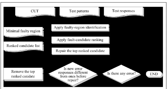
Figure 1 shows the overall flow of the proposed fault-diagnosis framework. Given the CUD, the test patterns, and the corresponding test responses obtained from the CUD, we apply the procedure, faulty-region identification, to report a minimal faulty region which covers all real faults. Then, the procedure, fault-candidate ranking, ranks the fault candidates within the faulty region based on the information collected during faulty-region identification. Next, we use the FIB technique to physically repair the fault candidate with the highest rank and then apply the same test patterns to the CUD. If the responses obtained from the repaired CUD are different from the
test responses obtained before the FIB repair, the repaired fault candidate is a real fault. Then we rerun the faulty-region identification and fault-candidate ranking based on the new obtained responses. Otherwise, the repaired fault candidate is not a real fault. Then we use the FIB technique to physically repair the next ranked fault candidate until a real fault is detected.
Key concepts:
In this subsection, we describe three key concepts used in our diagnosis framework: X-region, not-stuck-at-0 (or not-stuck-at-1) signals, and value-flipping technique.
1) X-region:
An X-region is a set of connected gates, whose logic values are set to unknown. When simulating failing patterns along with the unknown values in the X-region, we can determine whether the X-region covers all the real faults by comparing the simulated value on each failing output with the collected erroneous response. If the simulated value on any failing output is opposite to the value of its erroneous response, it means that the value on the failing output cannot be corrected no matter how the unknown values in the X-region are assigned. In such a case, this failing output must result from a fault outside the X-region and hence such an X-region does not cover all the real faults.
2) Not-stuck-at-0 & not-stuck-at-1 (NSA0 & NSA1):
Unlike other dictionary-based or region-based diagnosis methods, which attempt to identify a modeled fault or region matching the actual faulty syndrome, our diagnosis framework attempts to identify the signals which cannot be a fault, i.e., to identify the not-stuck-at-0 or not-stuck-at-1 signals. If a candidate signal can be proved that its value
on the defective chip is 0 (1) for any pattern, the candidate signal is then proved as a not-stuck-at-1 (not-stuck-at-0) signal. A candidate signal is guaranteed to be fault-free if this signal is proved to be both not-stuck-at-0 and not-stuck-at-1.
3) Value flipping on X-region’s boundary signals:
For each test pattern, we check whether a target signal on the X-region’s boundary is NSA0 or NSA1. A signal g is said to be on the boundary of an X-region if g ∈ X-region and there exists at least one g’s fan-out signal p, where p / ∈ X-region. We first calculate the good-circuit value v of the target signal through simulation. Then, we flip the value on the target signal to v’ and simulate the pattern again with all other boundary signals remaining the unknown value. If the simulated value on any output is different from its collected responses, then the target signal cannot be a stuck-at-v’ fault (or is NSAv’ ).
In the following, we explain our proposed methods about faulty-region identification and fault candidate ranking.
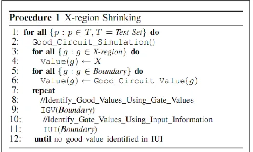
Faulty-region identification:
Figure 2 shows the X-region shrinking’s algorithm, and the algorithm attempts to identify the NSAv signals based on both passing and failing patterns. For each pattern, we first run good-circuit simulation to obtain the simulated good-circuit value for each signal (Line2). Second, we replace the value of signals within the X-region with the unknown value (Line3-6). Then, the sub-procedure IGV utilizes the value-flipping technique to check whether each signal on X-region’s boundary is NSAv0 if the simulated good-circuit value of the signal is v (Line9). During IGV, some boundary signals are identified to have the good value. Next, the sub-procedure IUI performs the backward and forward implication based on the new identified good values to further derive more good values on the boundary (Line11). We repeatedly perform IGV and IUI until no more good value can be found for the given pattern. The procedure IGV and procedure IUI are explain in the following.
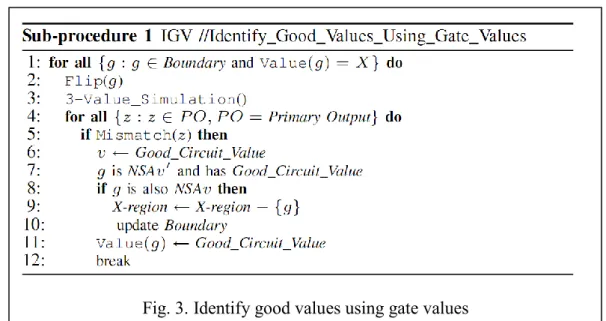
The detail steps of the sub-procedure IGV are listed in Figure 3. For each signal on X-region’s boundary with the unknown value, we first assign the signal’s value opposite to its simulated good-circuit value v (Line2), and then obtain the value-flipping value for each output through the 3-value simulation (Line3). Next, if there exists a simulated value-flipping value on any output different from its response
value, then the target signal is NSAv0 and guaranteed to have good value for the given pattern (Line5-7). We also check if the target signal has been recognized as a NSAv for previous patterns. If yes, then we remove it from the X-region (Line8-10). Last, we assign the value of the target boundary signal as the good
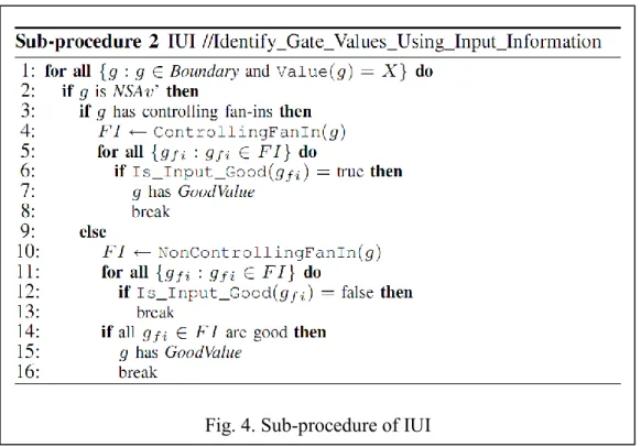
Figure 4 shows the detail steps of the sub-procedure IUI, which applies the implication technique and the value-flipping technique on the fanins of the boundary signals to further identify more boundary signals having the good value. Those new identified good values can then help the sub-procedure IGV in the next iteration to find more NSA0 and NSA1 signals. For each boundary signal with the unknown value, the sub-procedure IUI attempts to prove that this signal has the good value v, where v is the simulated good-circuit value for the given pattern. If the target signal has been proved NSAv0 and its fanins’ good values can propagate to the target signal, then the target signal has the good value. Two cases are discussed in the sub-procedure IUI to determine whether the signal’s fanins have the good value and
can propagate to the signal. If the simulated good-circuit value of any its fanin is the controlling value, then the target signal has the good value if any of its controlling fanin has the good value (Line4-8). Otherwise, the target signal has the good value if all of its non-controlling fanins have the good value (Line10-16).
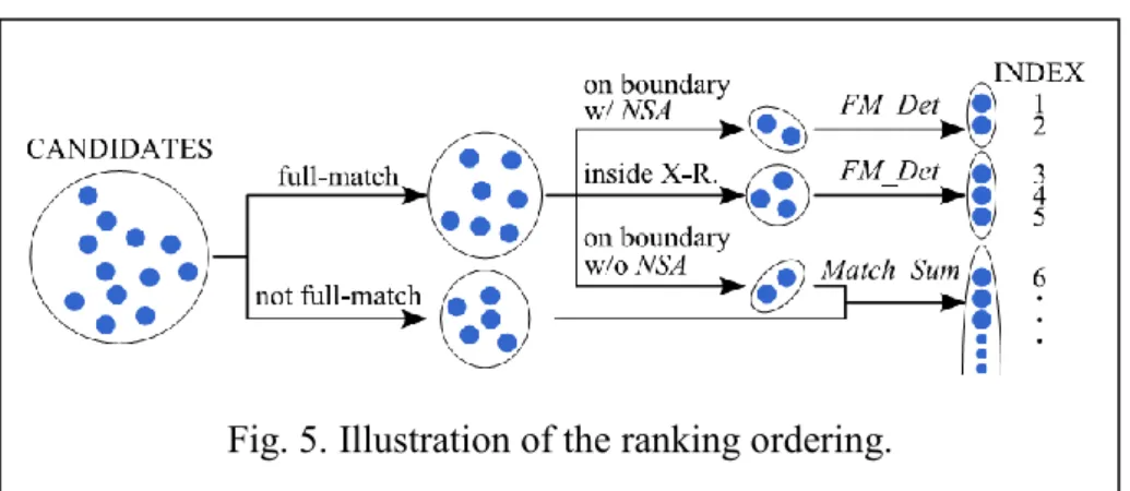
Fault candidate ranking:
Figure 5 summarizes our fault candidate ranking method. A fault c with at least one full-matched pattern is more likely to be a real fault than a fault without any full-matched pattern even if the fault c has less Match Sum(c). Therefore, our ranking method generally ranks the faults with a full-matched pattern higher than the faults without a full-matched pattern. We further divide the full-matching faults into three types, (1) the faults on the X-region’s boundary and the fault site is identified as a NSA0 or NSA1 signal during the X-region shrinking, (2) the faults inside the X-region, and (3) the faults on the X-region’s boundary and the fault site cannot be identified as a NSA0 or NSA1 signal during the X-region shrinking. A 1st-type fault ranks higher than the other two types because (i) a NSAv signal shows the possibility of generating a mismatch output from the fault site, and (ii) the existence of the 1st-type fault may be the reason why this fault site cannot be proved NSAv0. A 3rd-type fault ranks lower than the other two types because if the 3rd-type fault is the real fault
Experiments:
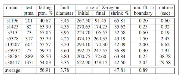
In the following experiment, we inject 3 nearby stuck-at faults at a time to sample a CUD, and then apply our diagnosis framework. Table I lists the average results after applying the proposed method over 100 sampled CUDs. Column 2 shows the number
of test patterns used in the experiments. Column 3 and 4 list the percentage of failing patterns and the fault diameter associated with the injected faults, respectively. The definition of the fault diameter is the maximum length of all the shortest paths on netlist between any two injected faults, which is used to measure the locality of the injected faults. Column 5 and 6 list the size of the X-region, that is the number of signals covered by the X-region, before and after applying the X-region-shrinking procedure, respectively. Column 7 lists the shrinking percentage from the initial X-region to the final X-region. Column 8 lists the minimum fault-to-boundary distance after applying the X-region shrinking, which is defined as the minimum netlist distance from an injected fault to the boundary of the final shrunk X-region. This minimum fault-to-boundary distance represents how effectively the X-region-shrinking procedure can reduce the X-region. The lower the distance, the better performance of the X-region-shrinking procedure. Last, Column 9 lists the runtime of the X-region shrinking in seconds.
As the result shows, the average shrinking percentage and minimal fault-to-boundary distance achieved by the X-region shrinking are 47.81% and 0.89, respectively. This result first demonstrates that the X-region shrinking can effectively eliminate the false candidate signals and minimize the suspect region such that the resulting X-region’s boundary is very close to real faults. Once the X-region’s boundary is reaching the real faults, it is difficult to further move the X-region’s boundary inward and the fan-in cones connecting to the real faults still remain in the X-region. Also, this result shows the efficiency of the X-region shrinking. The longest runtime among all benchmark circuits is 79.58 seconds (including the runtime of fault-candidate ranking).
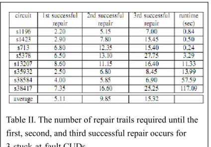
Table II shows the results of the fault-candidate ranking. Column 2, 3, and 4 list the number of repair trails required until the first, second, and third successful repair occurs, respectively. After a real fault is detected, we run the X-region shrinking again based on the new CUD, which removes the detected fault already. The runtime reported in the Column 5 is the sum of the runtime of each individual X-region shrinking and fault-candidate ranking. As the result shows, it requires in average 5.11,
Table II. The number of repair trails required until the first, second, and third successful repair occurs for 3-stuck-at-fault CUDs.
9.85, and 15.32 repair trails to hit the first, second, and third successful repair, respectively. It implies that almost 5 trials are required to hit a successful repair. Note that the equivalent faults are viewed as individual ones in our diagnosis framework and hence the reported results may not look as promising as it could be.
Diagnosibility for Silicon Debug
The first step of debugging is to infer the forward or backward implications according to the observed signals. We call these values to be conflict values, which are different between the implications and golden simulation values. By the conflict values, we can infer the values of other gates and sieve out the real location of errors. The more conflict values we can obtain from the forward or backward implications, the more diagnosibilities of a design has.
Due to the high complexity, the signals on-chip usually cannot be obtained from software simulation in limited time. In silicon debug, we have to do forward or
(a) (b)
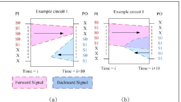
Fig. 5. The regions of forward and backward implications without and with intersection. (a) There is no intersection between these two regions. (b) The intersection region can help designers to infer the conflict values for debugging.
backward implications to find where the conflict values located from the limited signals we obtained. Thus, the diagnosibility in the silicon debug is defined by the number of the gates in the intersection between forward and backward implications. The more signals in the intersection, we have more chance to find the conflict values. For example, in figure 4, the signals obtained from forward implication are in pink region and the signals obtained from the backward implication are in blue region. Although there are more signals from forward and backward implications in figure 4 (a), there is no intersection of these two implications and we cannot obtain any conflict value. On the other hand, if there is any error, we could get the conflict values from the intersection of forward and backward implications of figure 6(b) and the diagnosibility of figure 6(b) is higher than figure 6(a).
Figure 7 shows the flow about computing the design diagnosibilty for silicon debug. First, given the netlsit without errors, we calculate the signal probability, P0
(P1), of the signal to be 0 (1). Then, with the signal correlations between flip-flops, we
can calculate the expected values of regions for forward and backward implications. Further, the expected values of the possible conflict region can be obtained from the intersection of the two regions for the design diagnosibility.
To calculate the possible implication region more accurate, the correlation of signals has to be concerned. The correlation between signals may suffer from the reconvergent fanouts or the same fanin cones of signals. Actually, the correlation exists in many signals in the same time and it is impossible to record all the
Calculate Signal Probability Calculate Expectation Value of Possible Conflict Region Netlist Observable signals and Unobservable signals Design Diagnosibility Signal probability and Signal correlation between flip-flops
correlations for each signal. In our calculations, we record the correlation for each pair of signals and, for approximation, the correlations of more than two signals are calculated from the correlation of signal pairs. Due to the approximation, the computation complexity becomes acceptable and the accuracy is higher than the calculation of independent probability for each signal.
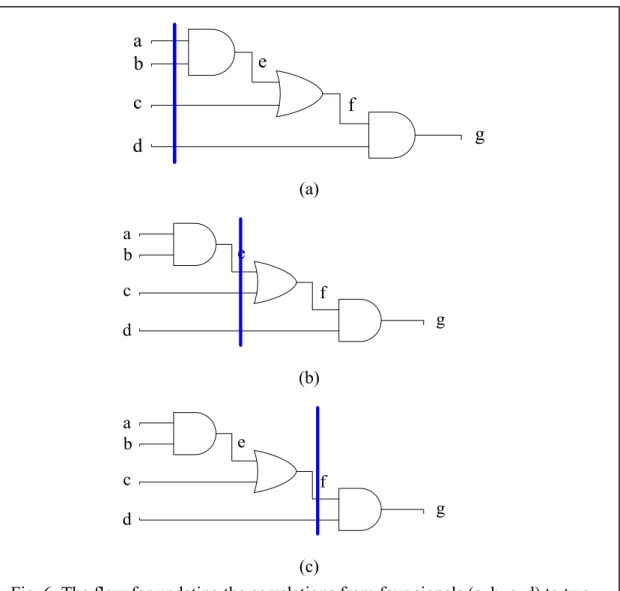
In figure 8(a), we already know the correlation for the signal lines, a, b, c, and d, as shown in the blue line. Once the P0 and P1 for signal e have been calculated from
a b c d e f g (a) a b c d e f g (b) a b c d e f g (c)
Fig. 6. The flow for updating the correlations from four signals (a, b, c, d) to two signals (f, d). (a) The signal correlations are between signal a, b, c, and d. (b) The correlations are updating to signals e, c, and d. (c) The correlation is updating to signals f and d.
signal lines of a and b, the correlations of a, b, c, and d will be updated to the correlations of e, c, and d, as shown in the blue line of figure 8(b). Similarly, when the P0 and P1 for signal f have been calculated from signal lines e and c, the correlation of
these signals will be updated to the correlation of f and d, as shown in the blue line in figure 8(c). Using the approximation of correlation for signal pairs, the signal probabilities of all signals are available for design diagnosibility.
Experiments:
We test our method on some ISCAS89 circuits and one result of s15850 is shown as following:
For first experiment as shown in table III, we set the probabilities, P0 and P1, of
each input to be both 0.5 and we calculate the probability from the inputs to the outputs and treat the circuit as a combinational circuit. After the calculation, we got the probability of P0 for this test circuit. Once we have the probability of P0, the
probability of P1 can be calculated easily. We show probability difference between the
calculation of our method and the results from simulation. In the first column, the Dffs mean the difference between filp-flops and the Outs means the difference between primary outputs. In the second column, the Max means the maximum difference among all Dffs or Outs. The third column, Min, means the minimum difference, and the last column, average, mean the average difference of all Dffs or Outs. From the experimental results, the Min differences are only from 1.1% to 1.2% and the average differences are from 2.1% to 3.6%, these results mean we can estimate the probability of P0 of each gate accurately.
S15850 Max Min Average Dffs 5.4% 1.1% 3.6% Outs 3.9% 1.2% 2.1%
Table III. The experiment results for S15850, we calculate the probabilities of all filp-flops and primary outputs from inputs to outputs one time and treat it as a combinational circuit.
For the second experiment as shown in table IV, the settings are the same as the first one, but we use the probabilities of the outputs to be the probabilities of inputs for next round if the signals are looped from some filp-flops. As we can see, the average differences are from 16.1% to 16.5% because we have the bigger estimation errors in Max differences. For Min difference, the differences are from 2.7% to 3.5%, and are still acceptable.
Layout Adjustment for FIB Technique
Figure 7 shows the overall flow of the layout adjustment framework for FIB S15850 Max Min Average
6326 21.1% 3.5% 16.1% 6327 20.3% 2.7% 16.5% Table IV. We continue to calculate the probabilities of all filp-flops and primary outputs until them convergence.
probing. We adjust the circuit layout to maximize the probability that a signal can be observed by FIB probing. The layout adjustment is done through a few pre-defined actions, which moves a small portion of the existing metal lines to different metal layers with new vias, instead of performing a complete rerouting. Therefore, the proposed DFD framework can be applied in conjunction with any APR tool and its impact on the timing of critical paths is limited. Also, the proposed DFD framework can restrict the layout adjustment on only the non-timing-critical paths if modifying certain critical paths may violate their timing constraint.
For FIB probing, the location to be probed corresponds to a net in the design netlist, which can be reported from a diagnosis tool and its observed value is used to confirm the assumption of an error candidate. A net in the design netlist corresponds to several metal lines across different metal layers and connected with vias. In our framework, a net is FIB observable if any of its metal line can satisfy all of the following conditions: (1) an FIB hole can be dug with a given edge slope and reach the surface of the line, (2) no other metal lines originally locate in the dug hole, (3) the target line lays in the middle of the hole’s baseline window, and (4) the overlap between the target line and the hole’s baseline window exceeds the given minimal sufficient width.
In the proposed framework, we adjust the layout based on only two basic operations, named move-up and move-down. Each operation is performed on a metal line of a net. As its name, a move-up operation will move a portion of the target metal line to a higher layer with extra vias. The function of this move-up operation is to create a long-enough metal line at a higher layer to successfully land an FIB hole on it when the original target line at a lower layer is blocked by other metal lines on top. As a result, the moved-up portion of a line must be longer than the minimal sufficient width of a baseline window.
Figure 8 illustrates an example of using a move-up operation, where metal line b is originally unobservable in Figure 8(a) since metal line a blocks the space on top of b for digging a sufficient FIB hole (as shown by the dashed shape). After applying a move-up operation to b in Figure 8(b), the moved-up portion of b can successfully land a sufficient FIB hole and hence b becomes observable. On the other hand, a move-down operation will move the target metal line to the empty space on a lower layer with vias. The function of this move-down operation is to remove the target line which originally blocks the observation of other lines below it, such that certain lines below it may become observable after the move-down operation.
Figure 9 illustrates an example of using a move-down operation, where line b is Fig. 8. Moving-up operation.
originally unobservable due to line a and c blocking the space above b as shown in Figure 9(a). After applying a move-down operation to a, line b becomes observable as shown in Figure 9(b).
The move-up and move-down operations need not necessarily be applied
individually. They can be applied together to make an unobservable line observable as illustrated in Figure 10, where line c is originally unobservable in Figure 10(a). After applying move-down operation to b and move-up operation to c, line c becomes observable in Figure 10(b).
Note that the move-up and move-down operations move the metal line only vertically, and hence the total metal length of the layout is almost the same, except that an extra length of a via needs to be added to connect the new via if only a portion of the line is moved. Also, all made move-up or move-down operations must be feasible, i.e., following the design rules, such as the spacing between the moved metal line and its new neighbors. In addition, some process technologies do not allow stacked vias, meaning that a via can pass through only a certain number of metal layers (3 in the UMC 90nm technology used in our experiments), which is another constraint of using a move-up or move-down operation.
The objective of this framework is to maximize the FIB observable rate without Fig. 10. Using both moving-up and moving-down operations.
violating any design rule or timing constraint. After parsing in the input files, the first step of the framework is to examine whether each metal line in the layout is FIB observable or unobservable. Among the unobservable lines, we further determine whether an unobservable line can become observable by using the basic operations, assuming all other layout remains the same. If yes, we consider how many operations are required. Those unobservable lines which can potentially turn into an observable one through basic operations are defined as the potentially observable lines. Based on the classification of all metal lines, we can determine whether a net is observable, potentially observable, or unobservable. Note that a net is (potentially) observable if any of its lines is (potentially) observable.
Next, our framework will iteratively select an untried potentially observable net and adjust the layout to turn it into an observable one until no untried potential exists. In fact, adjusting the layout for a potentially observable net may eliminate the chance of other potentially observable nets becoming an observable one. Therefore, in order to maximize the FIB observable rate, we need to find a proper order for the potentially observable nets being processed. In our framework, this process order of the potentially observable nets is determined by a proposed ranking method. Note that the layout adjustment here is performed based on a greedy-based principle. In other words, if an adjustment for a potentially observable net may turn an originally observable net into an unobservable or potentially observable one, the adjustment will not be performed. Any made layout adjustment must increase the overall FIB observable rate.
After the layout adjustment stops, we will perform connection check, design-rule check, and equivalence check to guarantee the correctness of the adjusted layout. Then we perform the RC extraction for the layout. Last, a timing analysis is applied based on the RC information, design netlist, and technology files. If any timing violation occurs, we will rerun the whole framework without adjusting the
timing-violated nets and the critical paths (if setup-time violated). In practice, timing violations rarely occur after our layout adjustment.
Experiments:
Table V reports the FIB observable rate based on a 1000nm minimum sufficient width of the baseline window and a 1-to-10 edge slope of an FIB hole. The cell-utilization rate is set to 80% to generate the initial layout with SoC Encounter. Also, dynamic ranking is used in MFOB to determine the order of nets for layout adjustment. In Table V, Column 1 and 2 list the circuit name and its total number of nets, respectively. Column 3 and 4 list the FIB observable rate before and after applying our proposed framework MFOB, respectively. Their difference is listed on Column 5. As the result shows, our proposed framework MFOB can successfully increase the FIB observable rate from 29.50% to 61.67% in average by properly adjusting the initial layout. The improvement in FIB observable rate ranges from 28.85% to 36.34% for different circuits. Column 6 of Table V lists the upper bound of the observable rate by using MFOB, which is actually the percentage of potentially observable nets estimated based on the initial layout. This upper bound can only be achieved when the layout adjustment for all the potentially observable nets will not
interfere with one another, which is not the case in practice. Hence, the true maximum observable rate that can be achieved is limited by the listed upper bound. As Table V reports, the difference between the observable rate of MFOB and the corresponding upper bound is 1.97% in average, showing that the observable rate achieved by MFOB is already not far away from the true maximum value. Column 7 of Table V lists the runtime of MFOB in seconds. The longest runtime is 290 seconds for a circuit with more than 16K nets.
Table VI reports the observable rate of the initial layout generated by setting the cell-utilization rate to 80%, 85%, and 90%, as well as its corresponding observable rate after applying MFOB. As the result shows, a higher cell-utilization rate always leads to a lower observable rate for the initial layout. Also, the observable-rate improvement achieved by MFOB is 32.17% (61.67-29.50), 31.53% (59.13-27.60), and 32.03% (57.75-25.72) for an 80%, 85%, and 90% cell-utilization rate, respectively. This result demonstrates that MFOB can still effectively improve the FIB observable rate for the layouts with different cell utilization rates.
Even though a move-up or move-down operation may add extra vias to a net, which increases its resistance, the circuit’s timing after applying our proposed framework usually becomes faster than its initial layout. Figure VII lists the longest path delay before and after applying MFOB, which is reported by a commercial timing analysis tool with the result of layout RC extraction. As the result shows, the timing after applying MFOB can indeed become faster than the timing of its initial layout for every benchmark circuit. Also, every modified layout passes the connection checking and equivalence checking.
四、 結論與討論
We proposed a diagnosis framework targeting multiple stuck-at faults. This framework utilizes the faulty-region identification to obtain a minimal suspect region covering all real faults, and the proposed ranking method ranks the fault candidates within the suspect region using the information obtained during the faulty-region identification. The experimental results demonstrate that the proposed diagnosis framework can effectively minimize the suspect region and its runtime is scalable to the circuit and the number of existing faults. In addition, the proposed framework requires no assumption on the number of existing faults as well as the size of the possible faulty region, which greatly increases the flexibility of its application.
For diagnosibility for silicon debug, we propose the flow to estimate the region of forward and backward implications and use an approximation method to calculate the correlation of each signal and the probability of every signal. The experimental results demonstrate we have very good approximation results in combination circuits.
We also proposed a DFD framework, which can increase the FIB observable rate by using a greedy-based algorithm to iteratively adjust the layout for a selected signal. A series of experiments have demonstrated that the targeted observable rate of the initial layout can be significantly increased without violating any design rule. Meanwhile, the adjusted layout can remain the same size and its timing can even become slightly better. In addition, the proposed frameworks can be easily integrated into the current design flow and applied in conjunction with any commercial APR tool.
五、 參考文獻
[1] M. Abramovici, P. Bradley, K. Dwarakanath, P. Levin, G. Memmi, and D. Miller, “A Reconfigurable Design-for-Debug Infrastructure for SoCs,” Design Automa-tion Conference, pp. 7–12, 2006.
[2] K.-H. Chang, I. L. Markov, and V. Bertacco, “Automating Post-Silicon Debug-ging and Repair,” International Conference on Computer-Aided Design, pp. 91–98, 2007.
[3] P. Bernardi, M. Grosso, M. Rebaudengo, and M. Sonza Reorda, “A Pattern Ordering Algorithm for Reducing The Size of Fault Dictionaries,” VLSI Test Symposium, pp. 386–391, 2006.
[4] I. Pomeranz and S. M. Reddy, “A Same/Different Fault Dictionary: An Extended Pass/Fail Fault Dictionary with Improved Diagnostic Resolution,” Design, Automation and Test in Europe, pp. 1474–1479, 2008.
on Computer-Aided Design of Integrated Circuits and Systems, vol. 18, no. 3, pp. 346–356, 1999.
[6] B. Arslan and A. Orailoglu, “Fault Dictionary Size Reduction Through Test Response Superposition,” International Conference on Computer Design, pp. 480–485, 2002.
[7] W. Zou, W.-T. Cheng, S. Reddy, and H. Tang, “Speeding Up Effect-Cause Defect Diagnosis Using a Small Dictionary,” VLSI Test Symposium, pp. 225–230, 2007. [8] Z. Wang, K.-H. Tsai, M. Marek-Sadowska, and J. Rajski, “An Efficient and Effective Methodology on The Multiple Fault Diagnosis,” International Test Conference, vol. 1, pp. 329–338, 2003.
[9] V. Boppana, R. Mukherjee, J. Jain, M. Fujita, and P. Bollineni, “Multiple Error Diagnosis Based on XLISTs,” Design Automation Conference, pp. 660–665, 1999. [10] A. L. D’Souza and M. S. Hsiao, “Error Diagnosis of Sequential Circuits Using Region-Based Model,” Journal of Electronic Testing, vol. 21, no. 2, pp. 115–126, 2005.
[11] Yu-Chin Hsu; Furshing Tsai; Wells Jong; Ying-Tsai Chang, "Visibility enhancement for silicon debug," Design Automation Conference, pp. 13-18, July 2006.
[12] Desineni, R.; Blanton, R.D., "Diagnosis of arbitrary defects using neighborhood function extraction," VLSI Test Symposium, pp. 366-373, May 2005.
[13] Savir, J; Ditlow, G S; Bardell, P H, “Random Pattern Testability,” IEEE TRANS. COMP. Vol. C-33, no. 1, pp. 79-90. 1984.
[14] Goldstein, L.H.; Thigpen, E.L., "SCOAP: Sandia Controllability/Observability Analysis Program," Design Automation Conference, pp. 190-196, June 1980.
[15] Reddy, P.V.C.V., "Testability measure and analysis," ASIC Conference and Exhibit, 1992., Proceedings of Fifth Annual IEEE International, pp.129-138, Sep 1992.
[16] M. Abramovici, P. Bradley, K. Dwarakanath, P. Levin, G. Memmi, and D. Miller, ”A Reconfigurable Design-for-Debug Infrastructure for SoCs”, Design Automation Conference, pp. 7-12, 2006.
[17] R. Goering, ”Post-Silicon Debugging Worth a Second Look”, EETimes, Feb. 05, 2007.
Boston, 2000.
[19] E. Anis and N. Nicolico, ”On Using Lossless Compression of Debug Data in Embedded Logic Analyis”, International Test Conference, pp. 1-10, 2007.
[20] E. Anis and N. Nicolico, ”Low Cost Debug Architecture using Lossy Compression for Silicon Debug”, Design Automation, and Test in Europe, pp. 1-6, 2007.
[21] J.-S. Yang and Nur A. Touba, ”Expanding Trace Buffer Observation Window for In-System Silicon Debug through Selective Capture”, VLSI Tset Symposium, pp. 345-351, 2008.
[22] C. Shawn, C. C. Tsao, and T. R. Lundquist, ”Measuring backside voltage of an integrated circuit”, U.S. Patent 6,872,581 B2, 2005.
[23] W.-M. Yee, M. Paniicia, T. Eiles, and V. Rao, ”Laser Voltage Probe (LVP): a Novel Optical Probing Technology for Flip- Chip Package Microprocessors”, Internation Symposium on the Physical and Failure Analysis of Integrated Circuits, pp. 15-20, 1999.
[24] M. T. Abramo and L. L. Hahn, ”The Application of Advanced Techniques for Complex Focused-Ion-Beam Device Modification”, Microelectronics Reliability, Vol. 36, Issues 11-12, pp. 1775-1778, 1996.
[25] C. G. Talbot, M. Park, N. Richardson, P. Alto, and D. Masnaghetti, ”IC Modification with Foucused Ion Beam System”, U.S. patent 5,140,164, 1992.
[26] D. C. Shaver and B. W. Ward, ”Integrated Circuit Diagnosis Using Foucused Ion Beams”, Journal of Vacuum Science & Technology B; Microelectronics and Nanometer Structures, Vol. 4, Issuse 1, pp. 185-188, 1986.
[27] R. Schlangen, R. Leihkauf, U. Kerst, C. Boit, and B. Kruger, ”Functional IC Analysis Through Chip Backside With Nano Scale Resolution - E-Beam Probing in FIB Trenches to STI Level”, International Symposium on the Physical and Failure Analysis of Integrated Circuits, pp. 35-38, 2007.
[28] J. Nonaka, ”Design for Failure Analysis by using LVP Measurement Elements”, Semi Technology Symposium, pp45-48, 2003.
[29] J. Nonaka, T. Ishiyama, and K. Shigeta, ”Design for Failure Analysis inserting Replacement-type Observation Points for LVP”, International Testing Conference, pp. 1-10, 2009.
[30] Y.-R. Wu, S.-Y. Kao, and S.-A. Hwang, ”Minimizing ECO routing for FIB”, VLSI Design Automation and Test, pp. 351-354, 2010.
[31] FEI Company, ”Focused Ion Beam Technology, Capabilites and Applications”, http://www.fei.com.
[32] Cadence, ”EncounderR User Guide,” version 8.1.2, 2009. [33] Synopsys, PrimeTime, version B-2008.12-SP3-2, 2009.
六、 計畫成果自評
These years, we have developed:
1) A new diagnosis algorithm based on faulty-region identification for silicon debug 2) A new ranking method for our diagnosis algorithm
3) A new flow to calculate the signal probability with signal correlations 4) An estimation method for approximated calculation about signal probability 5) A new layout-adjustment method to maximize the observation rate for FIB probing 6) A new ranking method for movable nets in our layout-adjustment method
Our works have been published on international journals and conferences, and the paper is listed as follows:
Megn-Jia Tsai, Mango C.-T. Chao, Jing-Yang Jou, Meng-Chen Wu “Multiple-Fault Diagnosis Using Faulty-Region Identification,” VLSI Test Symposium, pp. 123–128, 2009.
Kuo-An Chen, Tsung-Wei Chang, Meng-Chen Wu, Mango Chia-Tso Chao, Jing-Yang Jou, and Sonair Chen, “Design-for-Debug Layout Adjustment for FIB Probing and Circuit Editing”, accepted, International Test Conference, Sep. 2011.
Meng-Chen Wu, Hung-Ming Chen, and Jing-Yang Jou, “Mixed Non-Rectangular Block Packing for Non-Manhattan Layout Architectures,” International Symposium on Quality Electronic Design (ISQED), pp. 257-262, Mar. 2011.
Meng-Chen Wu, Ming-Ching Lu, Hung-Ming Chen, and Jing-Yang Jou, “Performance-constrained Voltage Assignment in Multiple Supply Voltage SoC Floorplanning,” ACM Transactions on Design Automation of Electronic Systems (TODAES), vol. 15, no. 1, Dec. 2009.
國科會補助專題研究計畫成果報告自評表
請就研究內容與原計畫相符程度、達成預期目標情況、研究成果之學
術或應用價值(簡要敘述成果所代表之意義、價值、影響或進一步發
展之可能性)
、是否適合在學術期刊發表或申請專利、主要發現或其
他有關價值等,作一綜合評估。
1. 請就研究內容與原計畫相符程度、達成預期目標情況作一綜合評
估
■ 達成目標
□未達成目標(請說明,以
100 字為限)
□實驗失敗
□因故實驗中斷
□其他原因
說明:
2. 研究成果在學術期刊發表或申請專利等情形:
論文:■已發表 □未發表之文稿 □撰寫中 □無
專利:□已獲得 □申請中 ■無
技轉:□已技轉 □洽談中 ■無
其他:
(以
100 字為限)
3. 請依學術成就、技術創新、社會影響等方面,評估研究成果之學
術或應用價值(簡要敘述成果所代表之意義、價值、影響或進一
步發展之可能性)(以
500 字為限)
我們在此子計畫中提出的兩個主要貢獻,錯誤分析以及針對 FIB
的繞線調整。前者可大幅降低錯誤診斷的時間成本,而後者則是
第一個提出對 FIB 來做繞線調整的技術。我們提出的方法皆可以
被整合進目前的設計流程之中,且不會對原有的設計或流程造成
太大的額外負擔。兩者在先進製程的測試階段皆有實質的影響,
隨著製成持續演進,預期未來還有更多的發展空間。
國科會補助計畫衍生研發成果推廣資料表
日期:2011/10/28國科會補助計畫
計畫名稱: 子計畫三:角落錯誤之矽除錯(3/3) 計畫主持人: 周景揚 計畫編號: 99-2220-E-009-010- 學門領域: 晶片科技計畫--整合型學術研究 計畫無研發成果推廣資料
99 年度專題研究計畫研究成果彙整表
計畫主持人:周景揚 計畫編號:99-2220-E-009-010- 計畫名稱:後次微米時代新興電子設計自動化技術之研究--子計畫三:角落錯誤之矽除錯(3/3) 量化 成果項目 實際已達成 數(被接受 或已發表) 預期總達成 數(含實際已 達成數) 本計畫實 際貢獻百 分比 單位 備 註 ( 質 化 說 明:如 數 個 計 畫 共 同 成 果、成 果 列 為 該 期 刊 之 封 面 故 事 ... 等) 期刊論文 0 0 100% 研究報告/技術報告 0 0 100% 研討會論文 0 0 100% 篇 論文著作 專書 0 0 100% 申請中件數 0 0 100% 專利 已獲得件數 0 0 100% 件 件數 0 0 100% 件 技術移轉 權利金 0 0 100% 千元 碩士生 4 5 80% 博士生 5 3 100% 博士後研究員 0 0 100% 國內 參與計畫人力 (本國籍) 專任助理 0 0 100% 人次 期刊論文 1 1 100% 研究報告/技術報告 0 0 100% 研討會論文 3 3 100% 篇 論文著作 專書 0 0 100% 章/本 申請中件數 0 0 100% 專利 已獲得件數 0 0 100% 件 件數 0 0 100% 件 技術移轉 權利金 0 0 100% 千元 碩士生 0 0 100% 博士生 0 0 100% 博士後研究員 0 0 100% 國外 參與計畫人力 (外國籍) 專任助理 0 0 100% 人次其他成果