Efficiency Improvement of Blue LEDs Using a
GaN Burried Air Void Photonic Crystal With
High Air Filling Fraction
Jia-Zhe Liu, Martin D. B. Charlton, Chung-Hsiang Lin, Kang-Yuan Lee,
Chirenjeevi Krishnan, and Meng-Chyi Wu
Abstract— In this paper, we investigate the efficiency
enhance-ment of blue InGaN/GaN light-emitting diodes (LEDs) by incor-porating a burried air void photonic crystal (BAVPC) layer within the epitaxial structure. As compared with the conventional patterned sapphire substrate (C-PSS) LEDs and flat sapphire substrate LEDs with BAVPC, the fabricated patterned sapphire substrate (PSS) LEDs with BAVPC exhibit the lowest full-width at half-maximum of (002) and (102) diffraction peaks, the highest light output power of 20.6 mW, and the highest external quantum efficiency of 37.4%. Remarkable performance improvement in the PSS LED with BAVPC is attributed to the better epitaxial quality with threading dislocations terminated by the BAVPC and the higher scattering at interface between GaN and air-void. By positioning the BAVPC directly below the multiple quantum wells (MQWs), it would cause the reduction in the number of trapped optical modes. The methodology optically isolates the MQWs from the underlying substrate and increases the optical output power. Moreover, threading dislocations are significantly suppressed using the BAVPC with high air filling fraction of
∼50%. It is well proposed that this methodology provides a
promising alternative to C-PSS LEDs.
Index Terms— Light-emitting diode (LED), burried air void
photonic crystal (BAVPC), patterned sapphire substrate (PSS), nanoimprint lithography (NIL).
I. INTRODUCTION
G
aN-BASED light-emitting diodes (LEDs) have diverse mass market applications including general illumination, full-color visual displays, traffic signals, and backlights forManuscript received December 19, 2013; revised February 17, 2014; accepted February 26, 2014. Date of publication March 11, 2014; date of current version March 19, 2014. This work was supported in part by Luxtaltek Corporation, in part by the National Tsing Hua University, in part by the Royal Society International Exchange Scheme, and in part by the National Science Council under Grants 101-2218-E-007-007 and 102-2218-E-007-002.
J.-Z. Liu is with the Institute of Electronics Engineering, National Tsing Hua University, Hsinchu 30013, Taiwan, and also with Luxtaltek Corporation, Miaoli 35059, Taiwan (e-mail: [email protected]).
M. D. B. Charlton and C. Krishnan are with the School of Electronics and Computer Science, University of Southampton, Southampton SO171BJ, U.K. (e-mail: [email protected]; [email protected]).
C.-H. Lin is with Luxtaltek Corporation, Miaoli 35059, Taiwan, and also with the Department of Photonics, National Chiao Tung University, Hsinchu 30010, Taiwan (e-mail: [email protected]).
K.-Y. Lee is with Luxtaltek Corporation, Miaoli 35059, Taiwan (e-mail: [email protected]).
M.-C. Wu is with the Institute of Electronics Engineering, National Tsing Hua University, Hsinchu 30013, Taiwan (e-mail: [email protected]).
Color versions of one or more of the figures in this paper are available online at http://ieeexplore.ieee.org.
Digital Object Identifier 10.1109/JQE.2014.2309137
liquid-crystal display panels. However, the overall efficiency of GaN-based LEDs is still limited due to low light extraction efficiency (LEE) and low internal quantum efficiency (IQE).
In order to improve the LEE, several approaches have been successfully proposed, such as surface texture on the p-GaN layer [1], [2], textured side walls [3], photonic crystals [4]–[10], and nanostructured LEDs [11]–[13]. On the other hand, various techniques have been developed to increase the IQE, such as trapezoidal well [14], electron block layer (EBL) [15], epitaxial lateral overgrowth (ELOG) [16], [17], InGaAlN/InGaN quantum well structures [18], non-polar GaN [19], GaN-nanowire [20], and quantum dot/wire/well hybrid LEDs [21]. However, previous research has focused on LEE or IQE. Recently, excellent progress has been made in simultaneously improving both the LEE and IQE. Methods include using patterned sapphire substrates (PSS) with a variety of proposed shapes [22], [23], novel epitaxial nanostructures [24]–[26], and GaN air-voids structures [27]–[30]. Those results demonstrate the superior light output power and the lower threading dislocation density.
In this study, we present a novel approach using a GaN burried air void photonic crystal (BAVPC) layer with a high air fraction of ∼50%, which not only enhances the LEE by internal reflection but also improves the IQE by the reduction of dislocation density. Most significantly, this technology can be effectively commercialized and provides a simple replace-ment to the conventional PSS (C-PSS) process.
II. EXPERIMENT
In this study, the epitaxial wafer was grown by metal-organic chemical vapor deposition (MOCVD) on the sapphire substrate with a VEECO K465i system. Firstly, a buffer layer of un-doped GaN (U-GaN) with a thickness of ∼30 nm was grown at 550 °C onto the c-plane (0001) flat sapphire substrate (FSS) and PSS. A layer of U-GaN with a thickness of∼3 µm was then grown onto the buffer layer at 1080 °C for both FSS and PSS. The chosen pattern of PSS has periodicity of 3µm with hexagonal lattice, spacing of 0.4 µm, and height of 1.6µm, which is the typical commercial design for PSS-LED substrates.
A BAVPC layer was formed by nanoimprint lithography (NIL) and reactive ion etching (RIE) as follows: A 200 nm thick SiO2layer was deposited by plasma enhanced chemical
vapor deposition (PECVD) onto the U-GaN epitaxial layer
0018-9197 © 2014 IEEE. Personal use is permitted, but republication/redistribution requires IEEE permission. See http://www.ieee.org/publications_standards/publications/rights/index.html for more information.
LIU et al.: EFFICIENCY IMPROVEMENT OF BLUE LEDs 315
surface as a hard mask, then a 200 nm thick polymer layer was spin-coated onto the top. A patterned silicon mold, fabricated by using electron-beam lithography, was then pressed into the polymer film. Whilst applying high pressure the substrate was heated above the glass transition temperature of the polymer. The substrate and mold were cooled down together to room temperature and the mold was released. The residual polymer layer was removed by RIE for 3-min etching time and then the defined pattern was transferred onto SiO2 layer by RIE.
The U-GaN layer was then etched by inductively cou-pled plasma ion etching (ICP-RIE) using a gas mixture of Cl2 and Ar. Finally, a buffered oxide etchant (BOE) was used
to remove the residual SiO2 layer. Related BAVPC process
can be referred in [6] and [25].
In our experiment, the BAVPC was chosen to be a square lattice with periodicity of 1 µm and a square air hole with width of 0.7µm giving an approximate air filling fraction of
∼50%. In order to optically isolate the BAVPC layer from the
underlying epitaxial substrate, the height of the BAVPC was chosen to be∼1.4 µm.
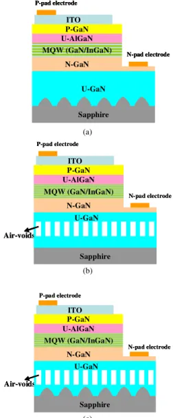
Subsequently, an epitaxial regrowth process was applied to the 2-inch test substrate incorporating the BAVPC, creating the final LED structure consisting of (i) a 2-µm-thick n-type GaN layer, (ii) six periods of InGaN (2.5 nm)/GaN (14 nm) multiple quantum well (MQW) active region, followed by (iii) a 10-nm-thick AlGaN EBL, and (iv) a 200-nm-thick p-type GaN layer. Silane, biscyclopentadienyl magnesium, and trimethylaluminum were used as n-dopant, p-dopant, and Al precursors, respectively. A C-PSS LED was also prepared with the identical epitaxial structure in the same epitaxial growth as the reference sample, in order to exclude the effect of run-to-run variability from the experimental results. Finally, the epitaxial wafers were diced with a chip size of 300 µm × 300 µm by standard photolithographic process. Schematic cross sections of the three types of LEDs are shown in Fig. 1.
III. RESULTS ANDDISCUSSION
Fig. 2(a) shows cross-sectional SEM image of epitaxial LED structure with BAVPC grown on PSS. Nano-columns between air-voids are approximately 1.4 µm high and 290 nm wide, and the air-voids are approximately 1.4 µm high and 700 nm wide. The thickness of epitaxial structure above the BAVPC is approximately 3.2µm. The cross-sectional SEM image of the epitaxial LED structure with a GaN BAVPC on FSS is shown in Fig. 2(b). An inspection of Fig. 2(a) and (b) reveals that both structures have almost identical layer thickness above the sap-phire substrates whether PSS exists or not. Fig. 2(c) shows the enlarged TEM image of the air-voids. It can be observed that threading dislocations (TDs) can only stretch from the bottom layer to the upper epitaxial LED structures in the GaN nano-columns. TDs would provide the leakage current pathway and non-radiative recombination centers, which cause LED performance deterioration. Observed from the TEM image of Fig. 2(d), the air-voids suppress the TDs and therefore improve the epitaxial quality and IQE.
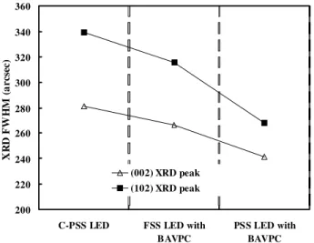
In order to further understand the improvement of epitaxial quality, Fig. 3 shows the full width at half maximum (FWHM)
Fig. 1. Schematic cross-sections of the three types of LEDs: (a) Conventional PSS LED (C-PSS LED), (b) FSS LED with BAVPC, and (c) PSS LED with BAVPC.
of high-resolution X-ray diffraction (HR-XRD) patterns using a PHILIPS X’Pert MRD system for the three LED configura-tions. It can be seen that the PSS LED with BAVPC (right-hand side of x-axis) exhibits the lowest FWHM of (002) and (102) diffraction peaks as compared to the C-PSS LED (left-hand side of x-axis) and FSS LED with BAVPC (centre of x-axis). The FWHM of (102) diffraction peak is related to the densities of TDs and edge dislocations [31], [32]. In addition, the FWHM of the (002) diffraction peak depends on screw and mixed-type dislocations. The FWHM of (002) diffraction peak is 281, 266, and 241 arcsec for C-PSS LED, FSS LED with BAVPC, and PSS LED with BAVPC, respectively. The FWHM of (102) diffraction peak is 339, 316, and 268 arcsec for C-PSS LED, FSS LED with BAVPC, and PSS LED with BAVPC, respectively. Both results show that the PSS LED with BAVPC possesses the best epitaxial quality with the lowest dislocation density. The improved epitaxial quality is attributed to the termination of dislocations under the air-voids array. It shows that our designed BAVPC can effectively
Fig. 2. Cross-sectional SEM and TEM images of epitaxial LED structures: (a) and (b) are SEM images of epitaxial structures with BAVPC grown on PSS and FSS, respectively; (c) and (d) are enlarged TEM images with BAVPC.
Fig. 3. FWHMs of (002) and (102) XRD peaks for three LED configurations.
alleviate the dislocation and obtain better epitaxial quality, which is in good agreement with the observations from SEM and TEM images.
Fig. 4(a) shows the light output power and voltage as a function of injection current for the three types of fabri-cated LEDs. When the current injection increases from 10 to 160 mA, the PSS LED with BAVPC exhibits outstandingly better light output power as compared to the C-PSS LED with BAVPC and FSS LED with BAVPC. At the forward injection current of 20 mA, the output powers are 18.4, 19.5, and 20.6 mW, and the forward voltages are 3.00, 3.00, and 3.06 V for C-PSS LED, FSS LED with BAVPC, and PSS
Fig. 4. (a) Light output power and voltage as a function of injection current for the three types of fabricated LEDs. (b) EQE and peak wavelength as a function of injection current for the three types of fabricated LEDs.
LED with BAVPC, respectively. At the high current injection of 160 mA, the output powers are 77.6, 82.2, and 86.7 mW, and the forward voltages are 4.23, 4.17, and 4.29 V for C-PSS LED, FSS LED with BAVPC, and PSS LED with BAVPC, respectively. The leakage current (IR) at a reverse bias of −6 V for the PSS LED with BAVPC and FSS LED with BAVPC are 0.004 and 0.026µA, respectively, which are clearly better than that of the C-PSS LED. The results confirm that the leakage current can be decreased by using BAVPC technique due to the reduction of dislocations. The wall-plug efficiency (WPE) is improved by 6% for FSS LED with BAVPC and further improved by 10% for PSS LED with BAVPC as compared with C-PSS LED.
Fig. 4(b) shows external quantum efficiency (EQE) and peak wavelength as a function of injection current for the three types of fabricated LEDs. When the current increases from 20 to 50 mA, the peak wavelength has a slight blue-shift of 0.62, 0.59, and 0.34 nm, respectively, for the C-PSS LED, FSS LED with BAVPC, and PSS LED with BAVPC. The less blue-shift for PSS LED with BAVPC could be attributed to the
LIU et al.: EFFICIENCY IMPROVEMENT OF BLUE LEDs 317
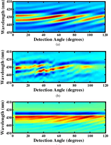
Fig. 5. Angular reflectivity maps for (a) C-PSS LED, (b) PSS LED with BAVPC, and (c) FSS LED with BAVPC.
reduction of the piezoelectric field-induced quantum confined Stark effect (QCSE) by strain relaxation in epitaxial layer. Besides, it is found that the EQE of PSS LED with BAVPC is also higher than that of C-PSS LED and FSS LED with BAVPC as the current injection increases from 20 to 160 mA. At the current injection of 20 mA, the EQE is 33.4%, 35.2%, and 37.4% for C-PSS LED, FSS LED with BAVPC, and PSS LED with BAVPC, respectively.
Performance improvement due to the incorporation of BAVPC can be attributed to both higher scattering at interface (GaN (n= 3.4)/air-void (n = 1)) and improvement in epitaxial quality at the same time, thus to increase the EQE and light output power. From the analyses of Figs. 2 and 3, the BAVPC effectively improves the epitaxial quality and results in better IQE. To understand the optical effect of BAVPC and its influence on LEE, numerical simulation for the three LED types and the optical mode mechanism are further investigated. Due to the high refractive index of GaN layer and the relatively thick epitaxial structure, LEDs suffer from poor light extraction for the high level of total internal reflection. In effect the epitaxtial layers form a highly multimoded waveguide. Trapped light becomes organized into well defined modes. Light which radiates from the surface, orginates from ‘leaky’ modes whose characteristic-mode angle is less than the critical angle for total internal reflection. Although these modes should in principle directly radiate from the LED surface, in practice a large amount of light becomes recyclced within the LED due to the high Fresnel reflection constant at the GaN/air interface. Recycled light therefore becomes organized into weakly confined Fabry-Perot (FP) modes.
The three LED structures were tested using a broadband spectroscopy with angular reflecometry system. This mea-sures the reflectivity of a highly collimated incident white Supercontinuum-Laser beam over a wide wavelength range. As in/out coupling of light to an LED is reciprocal in nature, this techinique provides us a detailed map of coupling char-acterisitics and accessible leaky FP modes of the device.
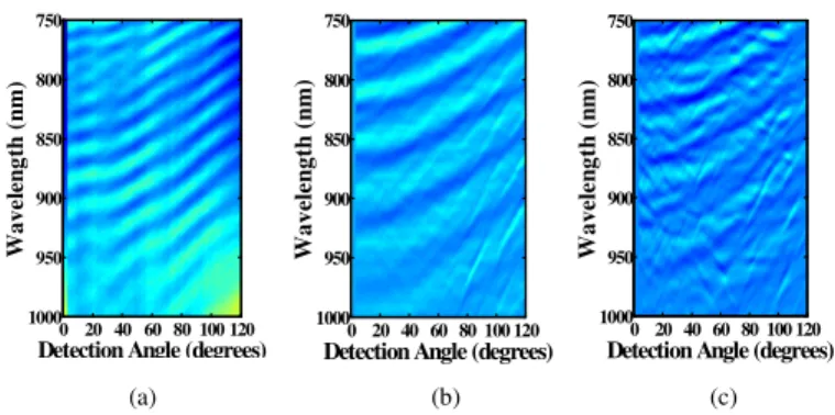
Fig. 5 shows the angular reflectivity maps for C-PSS LED, PSS LED with BAVPC, and FSS LED with BAVPC in the wavelength range of 450-950 nm. Color encodes the intensity of reflection at the specified incidence/reflection angle (both are the same). All plots are charachterized by a set of broad curved diagonal lines. These correspond to the weakly trapped FP modes of the LED substrates (note this experiment can-not access fully trapped modes lying below the light line).
Fig. 6. Broadband angular refelctivity maps for (a) C-PSS LED, (b) PSS LED with BAVPC, and (c) FSS LED with BAVPC to show the enhanced dispersive features associated with photonic crystal lattice arrangement of the air-voids.
The FP modes for C-PSS LED [42 total – Fig. 5(a)] are far more densly packed than those of PSS LED with BAVPC [24 total – Fig. 5(b)] and FSS LED with BAVPC [24 total Fig. 5(c)]. The number of FP modes relates to the effective thickness of GaN slab waveguide which can be accessed from the surface. The measurements show that the underlying air-viods can reduce the effective cavity size of slab waveguide by a factor of 1.75. The total epitaxial layer thickness for the FSS structure is about 5.9µm, whereas the thickness of GaN layers above the air-voids (which form the effective LED cavity) for PSS LED with BAVPC and FSS LED with BAVPC is about 3.2 µm (as shown in Fig. 2). These optical measurements therefore show that the effective cavity size is 3.4 µm and light becomes restricted to the region of GaN above the air-voids and the top 400 nm of the air-air-voids. This proves that this fabrication technique effectively isolates the light-emitting MQW layers at the top of LED from non-radiative optical modes and substrate modes. We also note that Fig. 5(c) (FSS LED with BAVPC) shows many other artifacts super-imposed on the FP mode structure.
Fig. 6 shows the broadband angular refelctivity maps for each LED type over a reduced wavelength range. In these plots, FP fringes have been digitally reduced in intensity (by applying a long range moving average filter) in order to enhance the fine dispersion features associated with the photonic crystal lattice arrangement of the air-voids. For the FSS LED with BAVPC [Fig. 6(c)], a very clear fine structure of sharp diagonal lines can be observed. It is arisen from the coherent reflections between neigbouring air-viods which overall cause the localization of light into well defined disper-sion bands. These photonic crystal bands provide additional leakage paths for the light from the top of the LED, and so enhance the light extraction by a secondary method. For the C-PSS LED [Fig. 6(a)], there is no evidence of photonic crystal dispersion. This is because the lattice pitch of the PSS is very large (5250 nm). PSS enhances the light extraction via a simple non-coherent reflection process [33]. PSS LED with BAVPC [Fig. 6(b)] shows the eveidence of photonic crystal dispersion, although much more weakly than the FSS LED with BAVPC.
Non-coherent, 3D finite-difference time-domain (FDTD) computer simulation was run for each LED type in order to understand the physical processes at play [34]. The simulation
Fig. 7. Computer simulation of optical power extraction as function of dipole launch angle for each LED type.
was setup to analyze the extraction enhancement on light reflected from the top GaN/air interface (no encapsulation), and so does not take into the microcavity effects (these are not relevant to this LED type as there is no metallic backside mirror). Simulation was carried out at the correct wavelength for the LEDs and it took into account full emission bandwidth as well as emission from multiple quantum wells.
Fig. 7 shows a computer simulation of radiative optical power intensity as a function of dipole emission angle. This plot gives a clear picture of optical emission behavior from what would otherwise be trapped modes lying below the light line. For the unpatterned FSS LED, there is no emission to free space at any angles below 65.5°. This angle corresponds to the critical angle for total internal reflection, and angles below this lie ‘below the light line’. At angles larger than the critical angle, light radiates to free space with increasing efficiency up to 90° (normal incidence). This gradual change in radiative power arises from angle dependent variation in Fresnel reflection coefficient at the GaN/air interface.
The solid blue trace shows light extraction behaviour of the C-PSS LED. This broadly follows the same extraction profile as the unpatterned FSS LED but is characterized by small modulations in radiative power (six small peaks). A small amount of recycled light is re-radiated from angles lying far below the light line (20-35°).
Plots for FSS LED with BAVPC and PSS LED with BAVPC are very nearly identical. In comparison to the unpatterned FSS LED within the normal light extraction cone (above the light line and critical angle), power extraction is modulated by 3 very distinct peaks. These contribute an additional radiated power (peaks have larger intensity and so lie above the the reference device curve). In comparison to the PSS device the number of peaks is reduced by a factor of 2 which is in line with the optical reflectivity measurements described in the previous section, and again confirms that light is confined mainly to the top half of the LED.
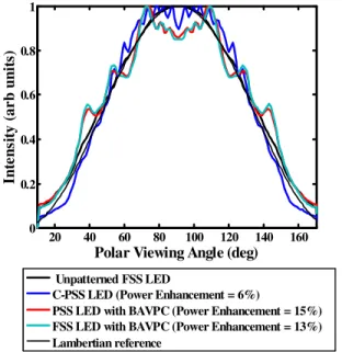
Fig. 8. Computational simulation of far-field beam profile for each LED type (power enhancement is shown in legend).
It is also observed that the additional power is extracted at angles just below the light line over the angular range of 50°–65°. Relative power extraction enhancement is shown in the legend of Fig. 7. The simulation shows that this particular design of C-PSS LED gives 6% improvement in light extrac-tion for the recycled light in comparison to unpatterned FSS LED without BAVPC, 13% improvement for FSS LED with BAVPC (7% improvement over C-PSS LED only), and 15% for PSS LED with BAVPC (2% improvement over FSS LED with BAVPC). These results are in very good agreement with the measured electroluminescent (EL) output power. Measured improvement in light output power for PSS LED with BAVPC (compared to FSS LED with BAVPC) is 6.4% at 20 mA. This includes an improvement in IQE of 3.95%. Actual measured improvement in optical extraction efficiency is therefore 2.4% which is very close to the simulation prediction. Performing a similar comparison between C-PSS LED and FSS LED with BAVPC, measured improvement in extraction efficiency is 0.25%, wheras the simulation predicts 6%. This is because the PSS geometry used in the simulation is not precisely the same as that fabricated (Simulation [device]: pyramid sidewall angle = 45° [60°], pitch 5.25 µm [4.5 µm], top epitaxial layer 2.9 µm [2 µm]). Actual extraction efficiency for PSS substrates is known to be highly dependent of the fine features of the geometry.
Fig. 8 shows the simulated far-field beam profile for each LED type, as well as a reference of unpatterned FSS LED, and a Lambertian reference. The unpatterned FSS LED follows the Lambertian curve very closely. This confirms that the simulation is well setup. The fine features on the curves for PSS and hole substrates follow the same trend as the previous discussion on power extraction, i.e., there are a number of additional clear peaks in intensity. The angular range at which they occur is in this case expanded due to the refraction at the top GaN/air interface in accordance with Fresnel’s law.
LIU et al.: EFFICIENCY IMPROVEMENT OF BLUE LEDs 319
Fig. 9. Angular electroluminescence measurements for (a) C-PSS LED, (b) PSS LED with BAVPC, and (c) FSS LED with BAVPC (x-axis range is from 0° (normal incidence) to 60° (marked 120° on plot)).
Fig. 9 shows the angle resolved emission spectum for each LED type. The C-PSS LED is characterized by 7 FP fringes over the emission range of 90°–30°, wheras the PSS LED with BAVPC has 4 distinct FP fringes over the same angular range. This is in line with the computational simulation (Fig. 8). FP firnges for FSS LED with BAVPC are partially broken up, showing the evidence of photonic crystal dispersion at the emission wavelength.
IV. CONCLUSION
We have successfully fabricated the blue LEDs incorpo-rating a BAVPC layer with a high air fraction of ∼50%, located just below the quantum wells on both FSS and PSS. We obtain the improvement in IQE and LEE for both LED types. At an injection current of 20 mA, the light output power of FSS LED with BAVPC and PSS LED with BAVPC increases by 6% and 10%, respectively, as compared to the C-PSS LED. These results are in good agreement with the FDTD simulation prediction. These photonic crystal bands provide additional leakage paths for the light from the top of the LED, and so enhance the light extraction by a secondary method. Broadband optical reflectometry measurements show that the BAVPC effectively isolates the underlying FSS or PSS substrate from the MQW region, greatly reducing the number of trapped modes into which the photons radiated in the MQW region. Beside, the analyses of XRD, SEM, and TEM show that the LEDs incorporating BAVPC grown
on FSS and PSS exhibit better epitaxial quality with threading dislocations terminated by the BAVPC.
REFERENCES
[1] S. Zhou, S. Liu, and H. Ding, “Enhancement in light extraction of LEDs with SiO2current blocking layer deposited on naturally textured p-GaN surface,” Opt. Laser Technol., vol. 47, pp. 127–130, Apr. 2013. [2] C. M. Tsai et al., “High efficiency and improved ESD characteristics of
GaN-based LEDs with naturally textured surface grown by MOCVD,”
IEEE Photon. Technol. Lett., vol. 18, no. 11, pp. 1213–1215, Jun. 26,
2006.
[3] C. S. Chang et al., “Nitride-based LEDs with textured side walls,” IEEE
Photon. Technol. Lett., vol. 16, no. 3, pp. 750–752, Mar. 2004.
[4] D. H. Long, I. K. Hwang, and S. W. Ryu, “Design optimization of photonic crystal structure for improved light extraction of GaN LED,”
IEEE J. Sel. Topics Quantum Electron., vol. 15, no. 4, pp. 1257–1263,
Aug. 2009.
[5] H. W. Huang, C. H. Lin, J. K. Huang, K. Y. Lee, C. C. Yu, and H. C. Kuo, “Improved light output power of GaN-based light-emitting diodes using double photonic quasi-crystal patterns,” IEEE Electron
Device Lett., vol. 30, no. 11, pp. 1152–1154, Nov. 2009.
[6] Y. C. Shin et al., “Effects of nanometer-scale photonic crystal structures on the light extraction from GaN light-emitting diodes,” IEEE J.
Quan-tum Electron., vol. 46, no. 9, pp. 1375–1380, Sep. 2010.
[7] H. Gao, K. Li, F. M. Kong, X. L. Chen, and Z. M. Zhang, “Improving light extraction efficiency of GaN-based LEDs by AlxGa1−xN confining layer and embedded photonic crystals,” IEEE J. Sel. Topics Quantum
Electron., vol. 18, no. 6, pp. 1650–1660, Dec. 2012.
[8] P. A. Shields et al., “Effect of coalescence layer thickness on the properties of thin-chip InGaN/GaN light emitting diodes with embedded photonic quasi-crystal structures,” Phys. Status Solidi A, vol. 209, no. 3, pp. 451–455, Mar. 2012.
[9] P. A. Shields, M. D. B. Charlton, T. Lee, M. E. Zoorob, D. W. E. Allsopp, and W. N. Wang, “Enhanced light extraction by photonic quasi-crystals in GaN blue LEDs,” IEEE J. Sel. Topics Quantum Electron., vol. 15, no. 4, pp. 1269–1274, Aug. 2009.
[10] M. Boroditsky, T. F. Krauss, R. Coccioli, R. Vrijen, R. Bhat, and E. Yablonovitch, “Light extraction from optically pumped light-emitting diode by thin-slab photonic crystals,” Appl. Phys. Lett., vol. 75, no. 8, pp. 1036–1038, Aug. 1999.
[11] J. H. Son, J. U. Kim, Y. H. Song, B. J. Kim, C. J. Ryu, and J. L. Lee, “Design rule of nanostructures in light-emitting diodes for complete elimination of total internal reflection,” Adv. Mater., vol. 24, no. 17, pp. 2259–2262, May 2012.
[12] M. Y. Ke et al., “Application of nanosphere lithography to LED surface texturing and to the fabrication of nanorod LED arrays,” IEEE J. Sel.
Topics Quantum Electron., vol. 15, no. 4, pp. 1242–1249, Aug. 2009.
[13] O. Lupan, T. Pauporté, and B. Viana, “Low-voltage UV-electro lumi-nescence from ZnO-nanowire array/p-GaN light-emitting diodes,” Adv.
Mater., vol. 22, no. 30, pp. 3298–3302, Aug. 2010.
[14] S. H. Han et al., “Improvement of efficiency droop in InGaN/GaN multiple quantum well light-emitting diodes with trapezoidal wells,”
J. Phys. D, Appl. Phys., vol. 43, no. 35, pp. 354004–354008, Aug. 2010.
[15] Y. Y. Zhang and Y. A. Yin, “Performance enhancement of blue light-emitting diodes with a special designed AlGaN/GaN superlat-tice electron-blocking layer,” Appl. Phys. Lett., vol. 99, no. 22, pp. 221103–221105, Nov. 2011.
[16] T. Mukai and S. Naksmura, “Ultraviolet InGaN and GaN single-quantum- well-structure light-emitting diodes grown on epitaxially laterally overgrown GaN substrates,” Jpn. J. Appl. Phys., vol. 38, pp. 5735–5739, Jul. 1999.
[17] H. Jia, L. Guo, W. Wang, and H. Chen, “Recent progress in GaN-based light-emitting diodes,” Adv. Mater., vol. 21, no. 45, pp. 4641–4646, 2009. [18] S. H. Park, Y. T. Moon, D. S. Han, J. S. Park, and M. S. Oh, “Light emission enhancement in blue InGaAlN/InGaN quantum well structures,” Appl. Phys. Lett., vol. 99, no. 18, pp. 181101-1–181101-3, Oct. 2011.
[19] S. F. Chichibu et al., “Origin of defect-insensitive emission probability in In-containing (Al,In,Ga)N alloy semiconductors,” Nature Mater., vol. 5, pp. 810–816, Sep. 2006.
[20] W. Guo, M. Zhang, P. Bhattacharya, and J. Heo, “Auger recombination in III-nitride nanowires and its effect on nanowire light-emitting diode characteristics,” Nano Lett., vol. 11, no. 14, pp. 1434–1438, Apr. 2011. [21] Y. H. Ko et al., “Electrically driven quantum dot/wire/well hybrid light-emitting diodes,” Adv. Mater., vol. 23, no. 45, pp. 5364–5369, Dec. 2011.
[22] M. T. Wang, K. Y. Liao, and Y. L. Li, “Growth mechanism and strain variation of GaN material grown on patterned sapphire substrates with various pattern designs,” IEEE Photon. Technol. Lett., vol. 23, no. 14, pp. 962–964, Jul. 2011.
[23] Y. B. Tao et al., “Evolution and control of dislocations in GaN grown on cone-patterned sapphire substrate by metal organic vapor phase epitaxy,”
J. Cryst. Growth, vol. 315, no. 1, pp. 183–187, Jan. 2011.
[24] T. Jung, L. K. Lee, and P. C. Ku, “Novel epitaxial nanostructures for the improvement of InGaN LEDs efficiency,” IEEE J. Sel. Topics Quantum
Electron., vol. 15, no. 4, pp. 1073–1079, Aug. 2009.
[25] H. W. Huang et al., “Efficiency improvement of GaN-based LEDs with a SiO2nanorod array and a patterned sapphire substrate,” IEEE Electron
Device Lett., vol. 31, no. 6, pp. 582–584, Jun. 2010.
[26] C. H. Kuo, Y. A. Chen, J. P. Wu, and L. C. Chang, “Efficiency improve-ment of near-ultraviolet nitride-based light-emitting-diode prepared on GaN nano-rod arrays by metalorganic chemical vapor deposition,” IEEE
J. Quantum Electron., vol. 50, no. 3, pp. 129–134, Mar. 2014.
[27] E. H. Park, J. Jang, S. Gupta, I. Ferguson, and C. H. Kim, “Air-voids embedded high efficiency InGaN-light emitting diode,” Appl. Phys. Lett., vol. 93, no. 19, pp. 191103-1–191103-3, Nov. 2008.
[28] C. H. Chiu et al., “Highly efficient and bright LEDs overgrown on GaN nanopillar substrates,” IEEE J. Sel. Topics Quantum Electron., vol. 17, no. 4, pp. 971–978, Aug. 2011.
[29] C. H. Chiu et al., “High efficiency GaN-based light-emitting diodes with embedded air voids/SiO2nanomasks,” Nanotechnology, vol. 23, no. 4, pp. 045303–045309, Feb. 2012.
[30] C. J. Lewins, D. W. E. Allsopp, P. A. Shields, X. Gao, B. Humphreys, and W. N. Wang, “Light extracting properties of buried photonic quasi-crystal slabs in InGaN/GaN LEDs,” J. Display Technol., vol. 9, no. 5, pp. 333–338, May 2013.
[31] B. Heying et al., “Role of threading dislocation structure on the x-ray diffraction peak widths in epitaxial GaN films,” Appl. Phys. Lett., vol. 68, no. 5, pp. 643–645, Jan. 1996.
[32] K. S. Kim et al., “Effects of growth rate of a GaN buffer layer on the properties of GaN on a sapphire substrate,” J. Appl. Phys., vol. 85, no. 12, pp. 8441–8444, Jun. 1999.
[33] M. D. B. Charlton, and S. Lin, “Optimization of pattern geometry and investigations of physical mechanisms contributing to improved light extraction in patterned substrate LEDs,” Proc. SPIE, vol. 7954, pp. 795419-1–795419-11, Feb. 2011.
[34] M. D. B. Charlton, P. A. Shields, D. W. E. Allsopp, and W. N. Wang, “High-efficiency photonic quasi-crystal light emitting diodes incor-porating buried photonic crystal structures,” Proc. SPIE, vol. 7784, pp. 778407-1–778407-8, Aug. 2010.
Jia-Zhe Liu was born in Kaohsiung, Taiwan, in
1985. He received the M.S. degree in electrical engineering from National Taiwan Ocean Univer-sity in 2008. He is currently pursuing the Ph.D. degree with the Institute of Electronics Engineering, National Tsing Hua University as well as a Senior Epitaxy Engineer with Luxtaltek Corporation. His main research interests include blue and UV light-emitting diodes and silicon solar cells.
Martin D. B. Charlton received the B.Sc. degree in
physics and electronics and the M.Sc. degree from the University of Reading, Reading, U.K., in 1991 and 1994, respectively, and the Ph.D. degree from the University of Southampton, Southampton, U.K., in 1999. He was the founder of a startup com-pany, Mesophotonics Ltd., Southampton, through which he commercialized work on photonic crystal devices, surface enhanced Raman scattering sensors, and high-brightness LEDs. He is currently with the University of Southampton, where he currently holds a Royal Society Research Fellowship with the School of Electronics and Com-puter Science. He is currently engaged in photonic crystals supercontinuum lasers, biosensing, and solid-state light sources. He received the Rank Thesis Prize in 1999 for the Ph.D. degree on fabrication and modeling of planar photonic crystal devices.
Chung-Hsiang Lin received the B.S. and M.S.
degrees in physics from National Taiwan University, and the M.S. degree in electrical and computer engineering and the Ph.D. degree in physics from the Polytechnic Institute of New York University, Brooklyn, NY. He is the President of New Busi-ness Unit with Luxtaltek Corporation and serves as an Adjunct Professor with the Institute of Electro-Optical Engineering, National Chiao Tung Univer-sity. He has over 10 years of experience in the LED industry, specifically photonic crystal modeling and nanofabrication on optoelectronic devices. He has over 30 professional publications related to photonic crystal devices. Before joining Luxtaltek, he held several research positions, including a Visiting Scholar with Jet Propulsion Laboratory, Pasadena, CA.
Kang-Yuan Lee received the B.S. degree in physics
from the National Sun Yat-sen University, Kaohsi-ung, Taiwan, and the M.S. and Ph.D. degrees in electrooptical engineering from National Chiao Tung University, Hsinchu, Taiwan, in 1996, 1998, and 2005, respectively. From 2000 to 2001, he was an Engineer with the Photo Lithography Division, Tai-wan Semiconductor Manufacturing Company Lim-ited. From 2006 to 2008, he was the Research and Development Section Manager with Asia Optical Corporation. He is currently with the Luxtaltek Cor-poration, Chunan, Taiwan. His research interests include optical measurement, GaN-based light-emitting device, and nanostructure fabrication.
Chirenjeevi Krishnan received the B.E. degree
in electronics and communication from Velammal Engineering College, Chennai, India, and the M.Sc. degree in nanoelectronics and nanotechnology from the University of Southampton, U.K., in 2009 and 2010, respectively, where he is currently pursuing the Ph.D. degree in hybrid LEDs and solar cells uti-lizing photonic crystals and resonant energy transfer.
Meng-Chyi Wu received the Ph.D. degree in
elec-trical engineering from National Cheng Kung Uni-versity, Taiwan, in 1986. He has over 30 years of research experience on III–V compound semi-conductors, material characterization, optoelectronic devices, and epitaxial techniques consisting of liquid-phase epitaxy, metalorganic chemical vapor deposition (MOCVD), and molecular-beam epitaxy. He is the first one to fabricate the red AlGaAs/InGaP light-emitting diodes in Taiwan, which help the development of visible LEDs grown by MOCVD. He also fabricated the long-wavelength InGaAsP/InP and AlGaInAs/InP laser diodes, which contain ridge-waveguide, distributed feedback, and vertical surface-emitting structures, for the fiber communication applications. He also fabricated the first InGaAs/InP and InGaP/GaAs p-i-n photodiodes (PDs) with high speed (10 GHz) and enhanced wide spectral range of 0.6–1.7 µm and 300–900 nm, respectively. The PDs permit the applications for high-speed communication, optical storage systems, such as CD-ROM, as well as red and blue laser DVDs. In addition, he also applied this p-i-n photodiode to integrate the ruby microball lens for the alignment tolerance enhancement. He has also developed the vertical organic thin-film transistors and transparent conductive oxides for the applications on the optoelectronic devices and displays. He has published over 270 journal papers on these research fields.