Spin-polarized electronic current in resonant tunneling heterostructures
A. Voskoboynikov, Shiue Shin Lin, C. P. Lee, and O. Tretyak
Citation: Journal of Applied Physics 87, 387 (2000); doi: 10.1063/1.371872
View online: http://dx.doi.org/10.1063/1.371872
View Table of Contents: http://scitation.aip.org/content/aip/journal/jap/87/1?ver=pdfcov
Published by the AIP Publishing
Articles you may be interested in
Spin-dependent transport and spin polarization in coupled quantum wells
J. Appl. Phys. 104, 064321 (2008); 10.1063/1.2981204
Fano Resonance and Spinpolarized Tunneling in a Magnetic Barrier Structure
AIP Conf. Proc. 850, 1502 (2006); 10.1063/1.2355273
Strong wave-vector filtering and nearly 100% spin polarization through resonant tunneling antisymmetrical magnetic structure
Appl. Phys. Lett. 81, 691 (2002); 10.1063/1.1495541
Asymmetrical spin-polarized tunneling and magnetoresistance in ferromagnet/insulator/insulator/ferromagnet junctions
J. Appl. Phys. 87, 2386 (2000); 10.1063/1.372190
Spin-polarized current in semimagnetic semiconductor heterostructures
Appl. Phys. Lett. 74, 2845 (1999); 10.1063/1.124033
Spin-polarized electronic current in resonant tunneling heterostructures
A. VoskoboynikovNational Chiao Tung University, 1001 Ta Hsueh Road, Hsinchu, 30010 Taiwan, Republic of China and Kiev Taras Shevchenko University, 64 Volodymirska Street, 252030 Kiev, Ukraine
Shiue Shin Lin and C. P. Leea)
National Chiao Tung University, 1001 Ta Hsueh Road, Hsinchu, 30010 Taiwan, Republic of China
O. Tretyak
Kiev Taras Shevchenko University, 64 Volodymirska Street, 252030 Kiev, Ukraine 共Received 27 October 1998; accepted for publication 6 October 1999兲
The spin-dependent tunneling phenomenon in symmetric and asymmetric resonant semiconductor heterostructures is employed in a theoretical study to investigate the output tunnel current polarization at zero magnetic field. A simple model of the resonant tunneling structures and a simple one-electron band approximation with spin-orbit interaction are used in this work. It is shown that asymmetry in the electron distribution at the electrode regions provides spin-polarized tunnel current. An approach to optimize this spin-dependent effect is explored theoretically. In asymmetric resonant tunneling structures, we estimate theoretically that the polarization can reach 40% with a moderate applied electric field. © 2000 American Institute of Physics.关S0021-8979共00兲09501-3兴
I. INTRODUCTION
Resonant tunneling structures 共RTSs兲 have been exten-sively investigated since the pioneering work of Tsu and Esaki and others.1–4 RTSs with a negative differential con-ductance are widely used in high frequency amplification, oscillation, fast switching, and logic functions. During an almost quarter-century-long history of research and develop-ment, the RTS has dealt with ‘‘nonspin’’ electrons only. Re-cently it has become clear that the employment of electron spin in tunneling processes can provide a new degree of free-dom in this area.5–7 The tunneling and resonant tunneling processes involving electron spin show prominent perspec-tives for new field-spin-dependent fast electronics. There are at least two areas of extensive research in spin-dependent tunneling and its associated phenomena. For example, spin-polarized scanning probe microscopy with an optical orien-tation of the tunneling electrons and tunneling spin valves is discussed extensively in the literature.8–10
In this article, we analyze the spin-dependent tunneling phenomenon in resonant tunneling structures. The spin-polarized electronic current is due to spin splitting of elec-tronic bands in asymmetric heterostructures.11–14The asym-metry in quantum well and quantum barrier heterostructures can be achieved technologically when the left and right bar-riers in the heterostructures are different. The asymmetry can also be obtained dynamically by applying an external electric field to the heterostructures. Spin splitting in the electron conduction band at zero magnetic field is a well-known prob-lem in connection with the fundamental physical character-istics of heterostructures. In asymmetric heterostructures with built-in or external electric fields, spin-orbit interaction provides coupling between spin and the electron’s spatial motion in the plane perpendicular to the direction of the
structure growth共in-plane motion兲. An advantage of this ap-proach is that the spin-dependent current can be controlled by an electric field. Theoretical and experimental investiga-tions have demonstrated the existence of the spin-splitting effect in asymmetric quantum well structures. Experimen-tally the spin-orbit splitting for electrons confined in hetero-structures has been studied by Raman scattering15–17 and Shubnikov-de Haas oscillation.18,19 Recently we found out that this effect is also strong in tunnel barrier structures and it can lead to the spin-dependent tunneling phenomenon.7
Advances in modern epitaxial growth technologies such as molecular-beam epitaxy 共MBE兲 and metalorganic chemi-cal vapor deposition 共MOCVD兲 have provided us with an opportunity to produce semiconductor heterostructures in which the material parameters can be changed over a wide range and controlled within considerable accuracy.20,21This level of quality allows the relevant theoretical analysis within the framework of relatively simple approximations for semiconductor band structures.22,23 So it is worthwhile to investigate how to obtain spin-polarized electronic current using the spin-spliting effect in the RTS.
In this article, the spin-dependent tunnel current in double-barrier heterosturctures is calculated. We show that to obtain the spin-polarized output electronic current we need asymmetry in the in-plane electronic wave vector distribu-tion. The asymmetry can be created by an additional in-plane electric field and we show that a measurable value of spin-polarized output electronic current is attainable. Two types of RTS are discussed: 共1兲 symmetric RTS (sRTS) and 共2兲 asymmetric RTS (aRTS). In aRTS we can obtain a polar-ization up to 40% with a moderate external electric field.
The article is organized as follows. In Sec. II some de-tails of the standard calculation of the electron spin-dependent tunneling probability in RTS are described. In Sec. III we propose a way to obtain spin-polarized output tunnel current in RTS and a method to evaluate the polariza-a兲Electronic mail: [email protected]
387
0021-8979/2000/87(1)/387/5/$17.00 © 2000 American Institute of Physics
tion. The calculated results of the symmetric and asymmetric RTS are presented in Sec. IV. In Sec. V we summarize pos-sible directions to optimize the effect.
II. SPIN-DEPENDENT TUNNELING PROBABILITY
A RTS with an external electric field Fz applied along
the direction of structure growth z is shown in Fig. 1. Layers of the structure are perpendicular to the z axis, and the in-plane electron wave vector is k关if k is put along an arbitrary x direction, the spin polarization is set along the y axis in the layer plane⫽(x,y)兴. In the structure there are two sources for the k-vector dependence of the transmission coefficient:
共1兲 through position-dependent energy band parameters 共like
in Refs. 24–29兲, and 共2兲 through the coupling between in-plane electron motion and the electron’s spin caused by the external electric field. The second one can lead to the spin polarization dependence in sRTS. The former leads to the spin dependent boundary conditions and manifests the spin-splitting effect in aRTS even without the presence of any external electric field.7,30,31 We use in our calculations the effective quasione-dimensional one-electron-band Hami-ltonian30,32 within the envelope function approximation.22 The total wave function of the electron⌽(z,) can be writ-ten as
⌽共z,兲⫽⌿j共z兲exp共ik•兲.
The wave function ⌿j(z) satisfies the z component of the
Schro¨dinger equation in the j th region:
Hj⌿j共z兲⫽E⌿j共z兲, 共1兲 where H1⫽⫺ ប2 2m1共E兲 d2 dz2⫹ ប2k2 2m1共E兲⫹E1c , when j⫽1; Hj⫽⫺ ប2 2mj共E兲 d2 dz2⫹ ប2k2 2mj共E兲 ⫹Ejc⫺eFz共z⫺z1兲 ⫺␣jkFz, when j⫽2⫺4; H5⫽⫺ ប2 2m5共E兲 d2 dz2⫹ ប2k2 2m5共E兲 ⫹E5c⫺eFzd, when j⫽5; 共2兲 1 mj共E兲 ⫽P 2 ប2
冋
2E⫺Ejc⫹Ejg⫹eFz共zj⫺z1兲
⫹E⫺E 1
jc⫹Ejg⫹⌬j⫹eFz共zj⫺z1兲
册
is position-dependent electronic effective mass in nonpara-bolic approximation, and ␣j is the Rashba spin-orbit
cou-pling parameter, the ‘‘second’’ contribution to the Rashba spin-orbit splitting:30 ␣j⫽ ប2 2mj共0兲 ⌬j Ejg 2Ejg⫹⌬j 共Ejg⫹⌬j兲共3Ejg⫹⌬j兲 .
In Eqs.共2兲 E denotes the total electron energy in the conduc-tion band, ⫽⫾1 refers to the spin polarization, d⫽z4
⫺z1 is total thickness of regions 2–4, and e is the electronic charge. The matrix element P is assumed to be z independent,22 and Ejc, Ejg, and ⌬j stand for the
conduction-band edge, the main band gap, and the spin-orbit splitting inside the jth region (E1c⫽0, conventionally兲 re-spectively. In the calculations, the nonparabolic approxima-tion Eqs.共2兲, for the electronic dispersion relations was used for all materials of the structures.7,30The role of the nonpa-rabolic approximation was discussed in Ref. 7.
The mass and spin-dependent boundary conditions for
⌿j(z) in an interface plane z⫽zj between j and j⫹1
re-gions were introduced in Ref. 30, 1 mj共E兲
再
d dzln关⌿j共z兲兴冎
z ⫽zj ⫺ 1 mj⫹1共E兲 ⫻再
dzd ln关⌿j⫹1共z兲兴冎
z⫽zj ⫽2k关j⫹1共E兲⫺j共E兲兴 ប2 , 共3兲 ⌿j共zj兲⫺⌿j⫹1共zj兲⫽0, where j共E兲⫽ P2 2冋
1E⫺Ejc⫹Ejg⫹eFz共zj⫺z1兲
⫺ 1
E⫺Ejc⫹Ejg⫹⌬j⫹eFz共zj⫺z1兲
册
is the position- and energy-dependent electronic spin-coupling parameters.
We calculate the spin-dependent transmission probabil-ity T(Ez,k) of the structure as a function of the
longitudi-nal component of the electron energy Ez and the in-plane
wave vector k. The relations among Ez, k, and the total
energy in view of the nonparabolicity can be found from the following expression:
FIG. 1. Variation of the semiconductor band parameters in a RTS under external electric voltage V.
388 J. Appl. Phys., Vol. 87, No. 1, 1 January 2000 Voskoboynikovet al.
E共Ez,k兲⫽Ez⫹
ប2k2 2m1共E,k兲
.
The well-known transfer matrix approach33 including spin-dependent boundary conditions 共3兲 are used to calculate T(Ez,k), as described in Ref. 31.
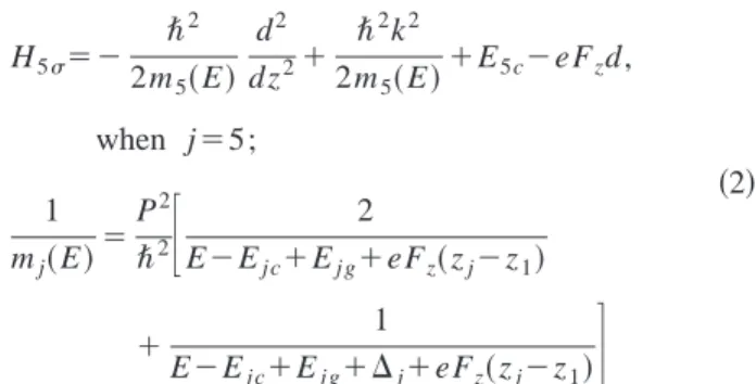
Before we present calculation of the spin-dependent tun-neling current, it is worthwhile to look at the characteristics of T(Ez,k). The spin-dependent tunneling probability T(Ez,k) shows a spin splitting of the resonant peaks in the (Ez⫺k) plane.30–32Those split up peaks correspond to the quasistationary levels with different electron spin polariza-tion in the RTS well. The splitting appears when there is asymmetry in the z direction in the structure. In sRTS the splitting is zero when Fz⫽0, and it increases with electric
field. As was found in Ref. 31 the splitting also exists for aRTS even without the presence of any external electric field. In Fig. 2 we present the split peak locations on the (Ez⫺k) plane for a sRTS consisting of two identical InAs–
GaAs–InAs barriers. Each barrier has a barrier width of z2
⫺z1⫽z5⫺z4⫽30 Å and a corresponding spacing between the barriers, z2⫺z3⫽60 Å under an external electric field of Fz⫽5⫻104 V cm⫺1.
The spin-split resonant tunneling probability provides a difference in resonance conditions for tunneling electrons with different directions of electron spin. We expect that the spin resonant peaks can render different contributions to the total electronic tunneling current in the RTS. Therefore, the spin-polarized output electronic current can be obtained.
III. POLARIZATION OF THE TUNNEL CURRENT
The value of practical interest is the polarization of the output tunnel electron current. We can estimate the polariza-tion of the electron tunnel current under electric field Fz
along the z direction for the tunnel structure with heavily doped electrodes shown in Fig. 1 as
p⫽J⫹⫺J⫺
J⫹⫹J⫺, 共4兲
where J⫽ e
83
冕
T共Ez,k兲关 f1共k兲⫺ f5共k兲兴u1zdkdkzis the tunnel current for the electrons with polarization, fj(k,kz) is the electronic distribution function in
three-dimensional兵k⫽(kx,ky);kz其 space in the emitter ( j⫽1) and
collector ( j⫽5) regions, u1z is the z component of the elec-tron velocity u1„k…⫽ 1 ប E k
in the emitter region.
According to the general features of the spin-orbit inter-action, Eqs. 共1兲 and 共3兲, the spin-dependent tunneling prob-ability T(Ez;k) satisfies the following relation of
symme-try:
T共Ez;k兲⫽T⫺共Ez;⫺k兲. 共5兲
It is easy to find out from Eqs. 共4兲 and 共5兲 that p⫽0 共no polarization in the total output current兲 if the electric field V⫽Fzd is applied along the z direction and the distribution f0(E) for electrons in the electrode regions is assumed to be Fermi like 关f1(k,kz)⫽ f0(E), f2(k,kz)⫽ f0(E⫹eV)兴. We can obtain the polarized output current only when the elec-tron distribution in the emitter region has asymmetry in the (kx,ky) in-plane intersection of the k space.
Let us assume that the total external electric field has an additional in-plane component, Fx. To avoid the influence
from this component on the tunneling probability described above we adhere to the condition Fx/FzⰆ1. Under an added
x component of the electric field the electron distribution becomes asymmetric in the (kx,ky) plane. Employing the
linear approximation on Fx we can treat the distribution
function by34
f1共k,kz兲⫽ f 共E,kx兲⬇ f0共E兲⫹e共E兲• f0共E兲
E •u1x共E兲•Fx,
共6兲
where(E) is the relaxation time for electrons and u1xis the x component of the electron velocity u1in the emitter region. For a degenerate electron gas with an Fermi energy Ef,f0(E)/E⬇⫺␦(E⫺Ef). Substituting Eq. 共6兲 into Eq.
共4兲, we get p共Fz,Fx兲⬇•I⫺ I⫹, 共7兲 where I⫺⫽
冕
1⫺ 1 共1⫺兲1/2d ⫻冕
0 /2 兵T⫹关Ef;kf共1⫺兲1/2cos兴 ⫺T⫺关Ef;kf共1⫺兲1/2cos兴其cosd,FIG. 2. Positions of the spin-split resonance tunneling probability peaks on the (Ez⫺k) plane for the symmetric RTS InAs–GaAs–InAs–GaAs–InAs 共the parameters are obtained from 共Refs. 23 and 35兲: E2c⫽E4c⫽0.792 eV,
E3c⫽E5c⫽0.0 eV, E1g⫽E3g⫽E5g⫽0.418 eV, E2g⫽E4g⫽1.52 eV, ⌬1
⫽⌬3⫽⌬5⫽0.38 eV, ⌬2⫽⌬4⫽0.341 eV, m1(0)⫽m3(0)⫽m5(0)
⫽0.023m0, m2(0)⫽m4(0)⫽0.067m0 (m0is the free electron’s mass兲, z2
⫺z1⫽z5⫺z4⫽30 Å, z3⫺z2⫽60 Å.
I⫹⫽
冕
1⫺ 1 d冕
0 共1⫺兲1/2 d ⫻冕
0 /2 兵T⫹共Ef;kfcos兲⫹T⫺共Ef;kfcos兲其 ⫻d, kf⫽ 1 ប冑
2m1共Ef兲Ef,⫽1Fx/u1(Ef), ⫽eV/Ef,1 is the electron mobility in the emitter region, and m1(Ef) is the electron effective mass
under the nonparabolic approximation 共2兲 at the Fermi en-ergy.
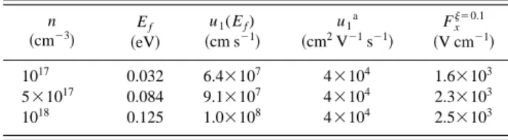
The unitless coefficientin Eq.共7兲 is used traditionally to verify the linear current theory’s 关Eq. 共6兲兴 applicability.34 To satisfy the linear theory condition, an appropriate value of the coefficient ⫽0.1 is used. In Table I each maximum allowable additional field Fx evaluated at ⫽0.1 for InAs
electrodes with different electron concentrations is presented. The fields as a whole satisfy the condition mentioned before (Fx/FzⰆ1), when Fz⭌0.5⫻104 eV cm⫺1.
IV. RESULTS AND DISCUSSION
First the polarized tunnel current in sRTS is discussed. As we demonstrated previously, the spin-split resonant peaks in the tunneling probability appear only with the presence of an external electric field Fz. The result of our calculation for
the tunnel heterostructures with a composition arrangement of InAs–GaAs–InAs–GaAs–InAs and different levels of
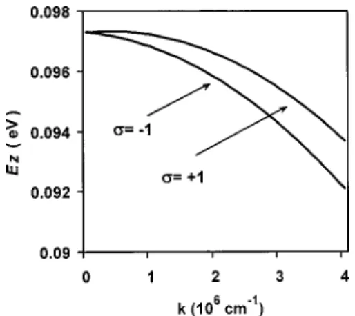
electron concentration is shown in Fig. 3. The curves present the total output electronic current polarization p(Fz) as a
function of the longitudinal electric field when⫽0.1. Two sharp peaks on the plots represent the highest level of the electronic output current polarization. The peaks’ appearance and position are clarified in Fig. 4 by the normalized total tunnel current along with the polarization curves for this structure having an electron concentration of 1017cm⫺3. We notice that the polarization peaks are situated at the begin-ning and the end of the tunnel current plot. The first peak appears when the Fermi level crosses the lowest spin-split quasistationary level in the well共see Fig. 2兲. The second one appears when the highest spin-split level 共with another spin polarization兲 crosses the bottom of the electronic band in the emitter region. This phenomenon allows us to optimize the magnitude of this effect.
To achieve a higher level of polarization, it is desirable to investigate aRTS with a built-in spin splitting of the reso-nant peaks in the tunneling probability.31 The external elec-tric field in these structures can amplify the splitting effect. From the description given above we can conclude that the
FIG. 3. Polarization of the total output tunnel current for the structure in Fig. 2 with different electron concentrations, n, in the electrodes. Curves
共a兲–共c兲 correspond, respectively, to the cases of n⫽1017, 5⫻1017, and 1018
cm⫺3.
FIG. 4. Normalized to their maximums are the total tunnel current (I⫹/I⫹max) and a polarization difference (I⫺/I⫺max) for the structure illus-trated in Fig. 2.
FIG. 5. Polarization of the total output tunnel current for the asymmetric structure InAs–GaAs–InAs–AlAs–InAs共the parameters are obtained from Refs. 23 and 35兲: E2c⫽0.792 eV, E4c⫽1.86 eV, E3c⫽E5c⫽0.0 eV, E1g
⫽E3g⫽E5g⫽0.418 eV, E2g⫽1.52 eV, E4g⫽3.13 eV, ⌬1⫽⌬3⫽⌬5⫽0.38
eV, ⌬2⫽0.341 eV, ⌬4⫽0.28 eV, m1(0)⫽m3(0)⫽m5(0)⫽0.023m0,
m2(0)⫽0.067m0, m4(0)⫽0.15m0, z2⫺z1⫽30 Å, z3⫺z2⫽50 Å, z4⫺z3
⫽15 Å. Curves 共a兲–共c兲 correspond, respectively, to the different electron
concentrations in the electrode regions: n⫽1017, 5⫻1017, and 1018cm⫺3.
TABLE I. Allowable additional electric fields for systems with different electronic concentrations n. n 共cm⫺3兲 共eV兲Ef 共cm su1(E⫺1f)兲 u1 a 共cm2V⫺1s⫺1兲 Fx⫽0.1 共V cm⫺1兲 1017 0.032 6.4⫻107 4⫻104 1.6⫻103 5⫻1017 0.084 9.1⫻107 4⫻104 2.3⫻103 1018 0.125 1.0⫻108 4⫻104 2.5⫻103 aReference 36.
390 J. Appl. Phys., Vol. 87, No. 1, 1 January 2000 Voskoboynikovet al.
resonant levels in the structure have to be situated in higher positions to employ the higher electric field in the beginning of the resonant current appearance. The same circumstance allows us to prefer systems with lower electron concentra-tions in the electrode regions. Based on those reasons we calculated the polarization in the asymmetric structures with configurations of InAs–GaAs–InAs–AlAs–InAs when z2
⫺z1⫽30 Å, z2⫺z3⫽50 Å, and z5⫺z4⫽15 Å. The calcula-tion results are shown in Fig. 5. The curves demonstrate an agreement with the general description of the spin-dependent effect presented above. The highest polarization is reached in a structure with an electron concentration of 1017cm⫺3and is above 40%. The sign of the polarization can be changed obviously by changing the direction of the additional in-plane electric field.
V. CONCLUSION
Research and applications of spin-dependent transport in semiconductor heterostructures often require spin-polarized electronic current.6 From this perspective, an active search for new opportunities to obtain spin-polarized output current in quantum heterostructures is essential. Semiconductor quantum heterostructures based on III–V semiconductors are well developed. An approach to control the spin-dependent transport in the structures without additional magnetic fields can be a potential advantage and it is worth investigating.
In this article, the spin-polarized tunneling current in resonant tunneling heterostructures at zero magnetic field was studied. We have theoretically demonstrated that asym-metry of the electron distribution in the electrode regions in RTS with spin-dependent tunneling probability can provide output tunnel current polarization. The polarization can be quite high for optimized structures. The effect is stronger for asymmetric RTSs with built-in spin splitting of the tunneling probability.
Finally, we want to point out that the calculation pre-sented uses a simple model of the resonant tunneling struc-tures and a simple one-electron-band approximation with spin-orbit interaction. The structures have realistic param-eters, but the proposed estimate of the total polarized current is only a starting point for the investigation of this new ef-fect. Further experimental investigations of the effects are really needed. Spin-dependent electronic transport that takes into consideration all accompanying de-polarization pro-cesses共elastic and inelastic兲 is the subject of special theoret-ical and experimental investigation.10 The development his-tory of RTS indicates that the implementation and optimization procedures require more complicated investigations.3
ACKNOWLEDGMENTS
This work was supported by the Ministry of Education of the ROC under Grant No. B87002, and by the National Science Council under Contract No. NSC 87-2215-E009-010.
1R. Tsu and L. Esaki, Appl. Phys. Lett. 22, 562共1973兲. 2
M. Y. Azbel, Phys. Rev. B 28, 4106共1983兲. 3
P. N. Racec, T. Stoica, C. Popescu, M. Lepsa, and Th. G. vau de Roer, Phys. Rev. B 56, 3595共1997兲.
4F. Capasso and A. Y. Cho, Surf. Sci. 299/300, 878共1994兲. 5A. Zakharova, Semicond. Sci. Technol. 13, 569共1998兲. 6
P. Bruno and J. Wunderlich, J. Appl. Phys. 84, 978共1998兲.
7A. Voskoboynikov, S. S. Liu, and C. P. Lee, Phys. Rev. B 58, 15397 共1998兲.
8H. J. Reittu, J. Phys.: Condens. Matter 6, 1847共1994兲. 9H. J. Reittu, J. Phys.: Condens. Matter 9, 10651共1997兲. 10
R. Jansen, M. W. J. Prins, and H. van Kempen, Phys. Rev. B 57, 4033 共1998兲.
11G. Dresselhaus, Phys. Rev. 100, 580共1955兲.
12Yu. A. Bychkov and E. I. Rashba, J. Phys. C 17, 6039共1984兲. 13
G. E. Pikus, V. A. Marushchak, and A. M. Titkov, Fiz. Tekh. Polupro-vodn. 共S.-Peterburg兲 22, 185 共1988兲 关Sov. Phys. Semicond. 22, 115 共1988兲兴.
14A. V. Kolesnikov and A. P. Silin, J. Phys.: Condens. Matter 9, 10929 共1997兲.
15
B. Jusserand, D. Richards, H. Peric, and B. Etienne, Phys. Rev. Lett. 69,
848共1992兲.
16D. Richards, B. Jusserand, H. Peris, and B. Etienne, Phys. Rev. B 47, 16028共1993兲.
17
B. Jusserand, D. Richards, G. Allan, C. Priester, and B. Etienne, Phys. Rev. B 51, 4707共1995兲.
18B. Das, S. Datta, and R. Reifenberg, Phys. Rev. B 41, 8278共1990兲. 19G. Engeles, J. Lange, Th. Scha¨pers, and H. Lu¨th, Phys. Rev. B 55, R1958
共1997兲. 20
D. K. Ferry and R. O. Grondin, Physics of Submicron Devices共Plenum, New York, 1991兲.
21Hot Carriers in Semiconductor Nanostructures: Physics and Applications, edited by J. Shah共Academic, New York, 1992兲.
22
G. Bastard, Wave Mechanics Applied to Semiconductor Heterostructures 共Les Edition de Physique, Les Ulis, France, 1990兲.
23S. L. Chuang, Physics of Optoelectronic Devices 共Wiley-Interscience, New York, 1995兲.
24B. Lee, Superlattices Microstruct. 14, 295共1993兲. 25
B. Lee and W. Lee, Superlattices Microstruct. 18, 178共1995兲. 26V. V. Paranjape, Phys. Rev. B 52, 10740共1995兲.
27X.-H. Wang, B.-Y. Gu, and G.-Z. Yang, Phys. Rev. B 55, 9340共1997兲. 28K. Miyamoto and H. Yamamoto, J. Appl. Phys. 84, 311共1998兲. 29M. Horak, Solid-State Electron. 42, 269共1998兲.
30
E. A. de Andrada e Silva, G. C. La Rocca, and F. Bassani, Phys. Rev. B
55, 16293共1997兲.
31A. Voskoboynikov, S. S. Liu, and C. P. Lee, Phys. Rev. B 59, 12514 共1999兲.
32
E. A. de Andrada e Silva, G. C. La Rocca, and F. Bassani, Phys. Rev. B
50, 8523共1994兲.
33E. O. Kane, Tunneling Phenomenon in Solids共Plenum, New York, 1969兲. 34N. M. Ashcroft and N. O. Mermin, Solid State Physics共Sounders College,
New York, 1976兲. 35
S. G. Shen and X. Q. Fan, J. Phys.: Condens. Matter 9, 3151共1997兲. 36Handbook Series of Semiconductor Parameters, edited by M. Livinshtein,
S. Rumyantsev, and M. Shur共World Scientific, Singapore, 1996兲, Vol. 1.