國立交通大學
電子物理研究所
以電漿輔助式分子束磊晶成長之氧化鎘鋅
薄膜在熱效應下的載子遷移過程研究
Thermal-Activated Carrier Transfer Processes in ZnCdO
Epilayer Grown by Plasma-Assisted Molecular Beam Epitaxy
研究生: 許維綸
指導教授: 周武清 教授
以電漿輔助式分子束磊晶成長之氧化鎘鋅薄膜在熱效應下的
載子遷移過程研究
Thermal-Activated Carrier Transfer Processes in ZnCdO Epilayer
Grown by Plasma-Assisted Molecular Beam Epitaxy
研 究 生:許維綸 Student:Wei-Lun Hsu
指導教授:周武清 教授 Advisor:Prof. Wu-ching Chou
國 立 交 通 大 學
電子物理系
碩 士 論 文
A Thesis
Submitted to Institute of Electrophysics College of Science
National Chiao Tung University in partial Fulfillment of the Requirements
for the Degree of Master in
Electrophysics June 2012
Hsinchu, Taiwan, Republic of China
i
以電漿輔助式分子束磊晶成長之氧化鎘鋅
薄膜在熱效應下的載子遷移過程研究
指導教授: 周武清 教授 研究生: 許維綸 國立交通大學電子物理所 摘要 本研究以分子束磊晶成長氧化鎘鋅薄膜,利用光激螢光與時間解析光譜 等技術來探討在溫度效應下氧化鎘鋅薄膜的載子躍遷行為。我們發現鎘摻 進氧化鋅後會在能帶中產生深淺不一的侷限態,當溫度升高時載子受聲子 散射的影響會從淺的侷限態躍遷至較深的侷限態發光,因此會造成螢光訊 號隨著溫度會有劇烈的紅位移現象,從時間解析光譜中可以明顯觀察到當 溫度升高時,載子隨著時間往低能量躍遷的現象,為載子躍遷提供了有利 的證據。 關鍵字:分子束磊晶、氧化鎘鋅ii
Thermal-Activated Carrier Transfer Processes in ZnCdO
Epilayer Grown by Plasma-Assisted Molecular Beam Epitaxy
Advisor: Prof. Wu-Ching Chou
Student: Wei-Lun Hsu Electrophysics
National Chiao Tung University
Abstract
The thermal-activated carrier transfer processes in Zn0.98Cd0.02O epilayer grown by molecular beam epitaxy was investigated by temperature dependent and time-resolved photoluminescence. The PL of ZnCdO alloy includes free exciton, deep and shallow localized states caused by fluctuations in Cd composition. We also verified the carriers are transferred to the deeper localized states when temperature increased. TRPL spectra gives a strong evidence about the thermal-activated carrier transfer processes in ZnCdO.
iii
Acknowledgement
感恩大家的幫忙,讓我順利完成兩年的碩士學業。由衷的感謝周老師兩 年來的指導,不僅指導我知識更提供我一個良好的學習環境,不論在學術 研究或待人處事上都讓我獲益良多。要特別感謝徐子民老師、陳衛國老師、 張文豪老師以及沈志霖老師在研究上給予我許多寶貴的意見。我要感謝當 我遇到困境時,會給予我協助的高雄大學的韓岱君老師、謝振豪老師,大 同大學的楊祝壽老師與岡山高中的陳培德老師。 我也要感謝一年多以來帶我的崑峰學長教導我許多長晶的技巧與經驗 的傳承。我要感謝實驗室的彥丞學長教導我使用實驗室的光譜系統也教我 如何游泳及把妹(雖然沒成功過),感謝李寧學長撥出自己寶貴時間幫我改 英文,讓我能在時間內完成這一分論文。感謝文忠、瑞泰與安傑學長教導 我如何使用實驗室儀器與分享實驗室的經驗。還有實驗室的偉仕、蓉霏、 侑霖、靜宜、家華、軒紹、湘穎、明叡還有小育,有了你們讓實驗室增添 許多的歡樂,讓我在碩士生涯充滿樂趣,祝福你們能在未來找到自己喜歡 的工作有個美滿的人生。 最後我還要感謝我的家人,如果沒有你們的支持我也沒有辦法心無旁鶩 的完成我的學業,還有我的女朋友,感謝你二十年來一直沒有出現,讓我 能專心的完成我的學業。藉著本論文的這頁感謝每一位照顧過我的人,願 我的家人、師長及好朋友們都能健康平安iv
Index
Abstract (Chinese version)... i
Abstract (English version)... ii
Acknowledgement... iii
Index…... iv
Chapter 1Introduction ... 1
1.1 Background... 1
1.2 Paper review of ZnCdO………... 2
1.3 Motivation…………... 4
Chapter 2 Experimants... 9
2.1 Molecular beam epitaxy (MBE) system... 9
2.2 Photoluminescence (PL) system... 11
2.3 Transmittance system... 12
2.4 Time-resolved photoluminescence (TRPL) system... 12
Chapter 3 Results and discussion... 19
3.1 Photoluminescence and transmittance study of ZnCdO... 19
3.2 Temperature dependent PL and T study of ZnCdO……... 19
3.3 Power dependent PL study of ZnCdO... 22
3.4 Time resolve photoluminescence (TRPL) spectra of ZnCdO.... 23
Chapter 4 Conclusion... 31
1
Chapter 1 Introduction
1.1 Background
Due to the concern of clean energy and green-house effect, the development of energy-saving devices is urgent. For illumination, the bright GaN-based light-emitting diodes1 (LED) gradually substitute the fluorescent lamps and bulbs. ZnO has similar physical properties as GaN. Both compounds have wurzite crystal structure and band gap close to 3.4 eV2. Recently, ZnO-based LED3 of high emission efficiency is reported. For the ZnO-based LEDs, the active layer is usually composed of ZnO/ZnMgO multiple quantum wells. Recently, ZnCdO/ZnMgO multiple quantum wells (MQW) are proposed to replace the ZnO/ZnMgO multiple quantum wells, because the introduction of Cd in ZnO not only provides the regulation of emission wavelength but also lattice constant. The band gap of ZnCdO alloys can be turned from ultraviolet to red light spectra4. The lattice constant can be adjusted to match the lattice constant of the ZnMgO barrier. Therefore, the study of growth and optical properties of ZnCdO is very interesting.
2 1.2 Paper review of ZnCdO
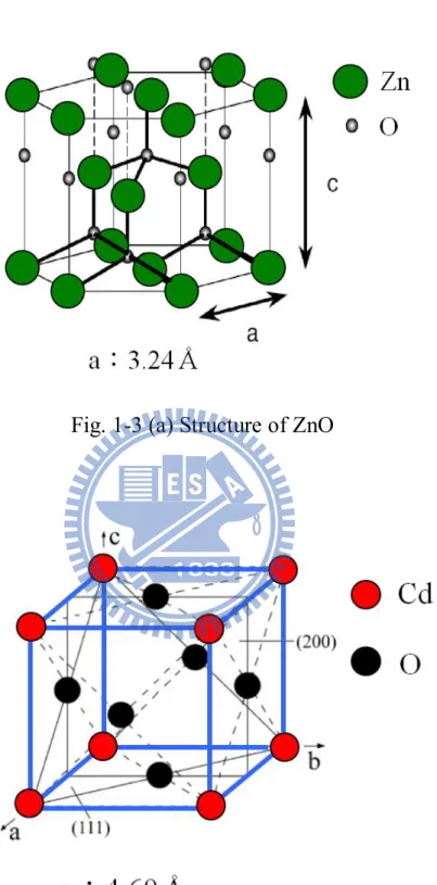
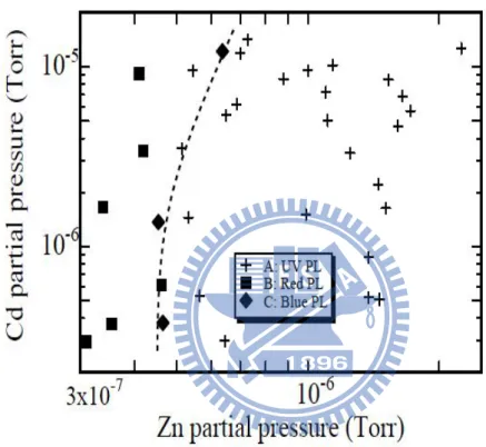
ZnO has a wurzite structure with the lattice constants a=3.25 Å and c=5.2 Å, as shown in Figure 1-1(a). ZnO is a semiconductor with a large bandgap of 3.4 eV and a large excitonic binding energy of 60 meV. Recent studies showed that the extremely stable excitons, which survive well above room temperature5. On the other hand, CdO has a rock-salt structure with the lattice constant a=4.69 Å, as shown in Figure 1-1(b). The direct optical band gap of CdO is 2.3 eV6.
The energy gap and lattice constants of ZnCdO and ZnMgO were studied by Makino and Kawasaki et al.7 in 2001, as shown in Figure 1-2. By choosing an appropriate combination of Cd and Mg concentrations, the growth of ZnCdO/ZnMgO MQW of perfect in-plane lattice match can be achieved, because both a-axis lattice lengths are monotonically increasing functions of Cd and Mg concentrations for both alloys. On the other hand, dependence of band gap energy on the Cd and Mg composition is opposite, the energy gap of ZnCdO decreases with Cd and the energy gap of ZnMgO increase with Mg. It results in a strong quantum confinement in the ZnCdO/ZnMgO MQW when both Cd and Mg are incresed. However, the fabrication of high quality ZnCdO epilayer is challenging.
3
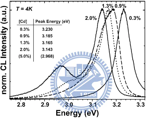
do not simply follow the partial pressures of Zn and Cd in molecular beam epitaxy (MBE). The obtained films were categorized in to three types, as shown in Figure 1-3. At relatively high Zn pressure, the luminescence is in the UV region (type A), same as pure ZnO films. At low Zn pressure, the luminescence turned to red (type B), similar to CdO films. At moderate Zn pressure of approximately 4~7×10⁻⁷ torr, films exhibited a blue luminescence peak (type C), which stand for ZnCdO alloy. There is only a narrow growth window of Zn/Cd composition ratio for the successful growth of high quality ZnCdO alloy.
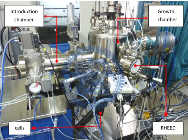
This narrow growth window for ZnCdO results from the difficulty of wurtzite phase ZnO crystallizing in the rock-salt structure CdO (Figure 1-1 a,b). The thermodynamic solubility limit of Cd in ZnO is 2%. The low solubility result was confirmed by Bertram et al.9. Their cathode-luminescence (CL) results showed that a low energy shoulder emerges when the Cd concentration was increased to 1.3%, as shown in Fig.1.4. As the Cd concentration was increased further to about 2%, two separate luminescence bands can be clearly distinguished with emission energies of 3.143 eV and 2.968 eV, respectively.
4 1.3 Motivation
Due to the difficulty to obtain high quality ZnCdO, many fundamental optical properties of ZnCdO are still not fully understood. In this thesis, the optical characteristics of the ZnCdO thin film grown by plasma-assisted MBE were investigated. The temperature-dependent PL and time-resolved PL (TRPL) were used to study the thermal-activated carrier transfer dynamics of ZnCdO.
5
Fig. 1-3 (a) Structure of ZnO
6
Fig. 1-2 Optical and structural properties of CdyZn1-yO and MgxZn1-xO alloy films mapped out in a plane of a-axis length and room-temperature band gap energy (Ref. 7)
7
Fig. 1-3 Obtained films, either type A, B or C, against partial pressures of Zn and Cd. (Ref. 8)
8
Fig. 1-4 Integrated CL spectra at T=4 K. The Cd concentrations and peak positions are summarized in the inset. (Ref. 9)
9
Chapter 2 Experiments
In this chapter, the experimental techniques used in this thesis are described, including molecular beam epitaxy, photoluminescence, transmittance, and time-resolved photoluminescence.
2.1 Molecular beam epitaxy (MBE) system
The SVT Associates molecular beam expitaxy (MBE) system is shown in Figure 2-1. It consists of a vertical growth chamber with ten sources, a load-lock chamber, and analytical equipment.
Currently, seven solid sources Zinc (Zn), Manganese (Mn), Cadmium (Cd), Magnesium (Mg), Chromium (Cr), Selenium (Se), Tellurium (Te), and Zinc Chloride (ZnCl2), and two gas sources, Oxygen (O2) and Nitrogen (N2), are operated each source has its own shutter to control the growth time. There is a main-shutter between sources and the substrate to avoid the unintentional evaporation before growth.
The load-lock chamber used to transfer substrate from air to the growth chamber and was maintained at 5×10⁻⁸ torr by using a dry rotary pump and a turbo molecular pump. The growth chamber was further pumped down to a base
10
pressure of 8×10⁻¹⁰ torr. The reflection high-energy electron diffraction (RHEED) system is also set up in the growth chamber. It is an invaluable tool to determine different aspects of the deposition layer. Morphological data of the surface may be interpreted from the spot and line pattern, which appear on the phosphor screen display during growth.
ZnO and ZnCdO thin films were grown on c-plane sapphire substrates. The group-II atoms were produced in conventional effusion cells by evaporating elemental Zn (6N), and Cd (6N). The group-VI atoms were supplied by introducing oxygen (5N5) gas through a rf-plasma source. Prior to the growth procedure, the substrates were degreased in acetone and methanol to clean up organic pollution, etched in a H2SO4:H3PO4=3:1 solution for 15 minutes at 160 o
C to remove the pollution of oxide, rinsed in flowing de-ionized water about two minutes and dried with high purity N2. After the substrate was transferred into the growth chamber it was desorbed at 850 oC and treated in oxygen plasma, which is expected to produce an oxygen terminated Al2O3 surface. In order to reduce the lattice mismatch between ZnCdO and Al2O3, we grow a 70 nm-thick ZnO at 650 oC as the buffer layer. The structure of our samples was shown in Figure 2-2 (a), (b). ZnO and ZnCdO epilayers with thickness of 480 nm were then grown at 450 oC. After growth, the optical characterizations of the samples
11
were analyzed by photoluminescence, transmittance and time-resolved photoluminescence at various temperatures.
2.2 Photoluminescence (PL) system
To study optical properties of semiconductors, laser beams with photon energy higher than the band gap energy of the semiconductor are usually used to excite electrons from the valence band to the conduction band and leave holes in the valence band. The excited (electrons/holes) relaxed to (bottom of the conduction band/top of the valence band) through the carrier-phonon interaction. Electrons and holes form exciton by Coulomb interaction. Electrons and holes, Excitons, recombination could emit photons and be detected by photoluminescence (PL) spectroscopy.
The experimental set-up for the photoluminescence measurement is shown in Figure 2-3. PL measurements were performed by using the 325 nm line of a He-Cd laser. The incident beam was focused by a lens (f=10 cm). The PL emission from sample was collected by second lens (f=10 cm) and focused by the third lens (f=30 cm) to the spectrometer. The signal was dispersed by an Ihr550 spectrometer and detected by liquid nitrogen cooled charge-coupled device (CCD). The spectrometer was controlled by a computer, which was used
12
to store and plot the collected data. For temperature-dependent PL measurements, samples were cooled in a closed-cycle refrigerator system. The temperature was varied from 10 K to 300 K.
2.3 Transmittance system
The experimental set-up for transmittance measurement is shown in Figure 2-4. A broadband xenon lamp was used as an excitation source. The incident beam was focused on the sample by a lens (f=10 cm). The transmittance beam from the sample was collected to the entrance slit by lens L2 (f=10 cm) and L3 (f=30 cm). The transmittance spectra were analyzed by the Ihr550 spectrometer and detected by liquid nitrogen cooled charge-coupled device (CCD).
2.4 Time-resolved photoluminescence (TRPL) system
TRPL system was used to study the decay dynamics of excitons. The experimental setup of TRPL system is similar to the PL system and shown in Figure 2-5. The GaN diode laser with 50 ps pulses and a repetition rate of 40 MHz at a wavelength of 377 nm was used as an excitation source. The peak power of the pulse was estimated to be below 0.1 mW. The laser beam was focused on the sample by a lens (f=10 cm). The combination lenses guide the
13
signal to the iHR550 spectrometer, which was equipped with a high-speed photomultiplier tube to detect the signal. The signal was further analyzed by a computer. The overall temporal resolution of the setup was about 300 ps.
14
Fig. 2-1 SVT Associates molecular beam expitaxy (MBE) system
Growth chamber Introduction chamber chamber cells RHEED
15 (a)
(b)
Fig. 2-2 (a) Schematic structure of ZnO thin film, (b) Schematic structure of ZnCdO thin film
Sapphire ZnO ZnCdO Sapphire ZnO ZnO
16 325 nm He-Cd laser CCD Laser line chamber sample F=10 cm F=30 cm F=10 cm 325 nm He-Cd laser CCD Laser line chamber sample F=10 cm F=30 cm F=10 cm
17
CCD
chamber
sample
F=30 cm
F=10 cm
xenon
lamp
F=10 cm
CCD
chamber
sample
F=30 cm
F=10 cm
CCD
chamber
sample
F=30 cm
F=10 cm
xenon
lamp
F=10 cm
xenon
lamp
F=10 cm
18
37
7 n
m
Ga
N
pu
lse
d
las
er
PMT
chamber
sample
F=10 cm
F=30 cm
F=10 cm
37
7 n
m
Ga
N
pu
lse
d
las
er
PMT
chamber
sample
F=10 cm
F=30 cm
F=10 cm
19
Chapter 3 Results and discussion
3.1 Low –temperature photoluminescence (PL) and transmittance
The PL and transmittance spectra of ZnO and ZnCdO at 10 K are shown in Figure 3-1(a), (b), respectively. Sharp near-band-edge emissions of ZnO at about 3.361 eV were observed, as shown in Figure 3-1(a). The emission peaks at 3.361 and 3.366 eV were assigned to the excitons bound to neutral donors10. Comparing with the absorption edge of the transmittance spectrum, the peak at 3.377 eV is attributed to the free A excitons (FXA)11. When Cd atoms were introduced into ZnO, the PL peak becomes broad and the energy position shifts to 3.185 eV. Fine structures of bound excitons could not be resolved. The PL peak position of ZnCdO can be written as
EPL = (3.35-9.19x+8.14x2) eV, (1)
according to the results of Gruber et al.14 The Cd composition of our sample is 2 %. Additionally, the PL emission profile of ZnCdO is not symmetry due to the existence of localized state at lower energy. The FXA state of ZnCdO was 3.265 eV, which was determined from the absorption edge of the transmittance spectra. 3.2 Temperature-dependent PL and transmittance
20
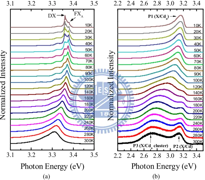
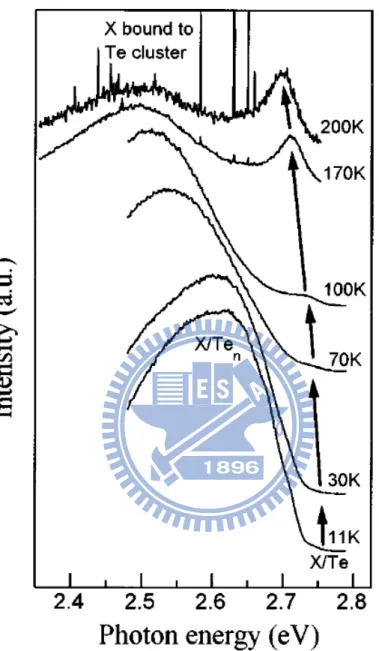
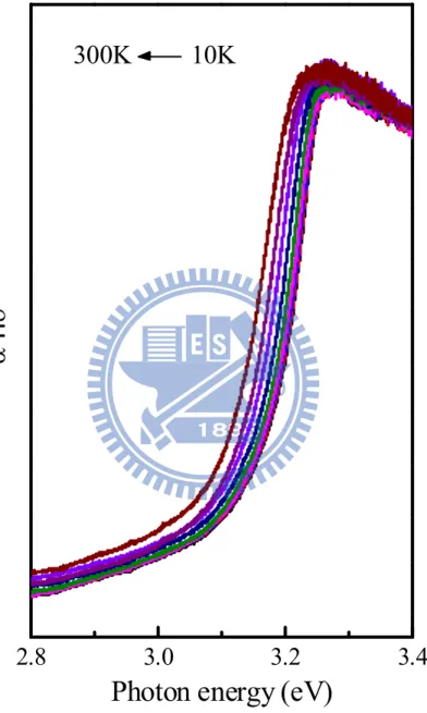
temperature dependent PL spectra were studied. In comparison, the temperature dependent PL spectra of ZnO were also carried out, as shown in Figure 3-2(a). Both DX and FXA in ZnO shift to lower energy and the line-width broadens with the increasing temperature. The broadening of PL band is related to the carrier-phonon interaction. Additionally, because carriers are thermally activated, FXA dominates at higher temperature. In case of ZnCdO epilayer, as shown in Figure 3-2(b), only one peak, P1, was observed at low temperature. The line shape of P1 is highly asymmetric. The lower energy shoulder consists of another emission band, which dominates the P1 emission band at higher temperature. When T >140 K, additional peaks, P2 and P3, become visible. The intensity of P2 increases and exceeds P1 when T > 240 K. The similar optical properties were observed by Yang et al.15 in ZnSe1-xTex (x=0.01) epilayers, as shown in Figure 3-3. In the case of ZnSe1-xTex at a low temperature of 10 K, the X/Te is not observed and the PL of the Ten-bound excitons (X/Ten) is very pronounced. The energy states of X/Te and X/Ten cluster becomes observable as the temperature was increased. Thus, the PL peaks of P1, P2, and P3 can be attributed to the emissions from X/Cd, X/Cdn, and X/Cdn cluster, respectively. In order to understand the properties of X/Cd and X/Cdn in ZnCdO, the temperature-dependent transmittance spectra of the ZnCdO were investigated as
21
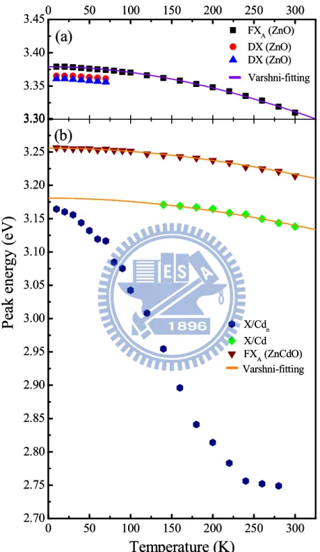
shown in Figure 3-4. The absorption edge shifts monotonically to lower energy as the temperature increases. The peak positions of the FXA, X/Cd, and X/Cdn emission as a function of temperature were plotted in Figure 3-5(b).
For ZnO, as shown in Figure 3-5(a), the energy positions of FXA and DX monotonically decrease as the temperature increases. The red-shift of these peaks with increasing temperature obeys the Vashinis' formula16, which is writing as
Eg(T) = Eg(0)-αT2/(β+T), (2)
where Eg(0) is the band-gap energy at T=0 K, and α and β are the corresponding thermal coefficients. On the other hand, for ZnCdO, as shown in Figure 3-5(b), only the trace of FXA and X/Cd obey the Vashinis' prediction. The PL spectra of X/Cdn and X/Cd emissions are more complicated, because the X/Cdn and X/Cd emissions are attributed to the localized states emissions due to high fluctuation in Cd composition.
22 3.3 Power dependent PL study of ZnCdO
Figure 3-6 shows the power dependent PL spectra at 220K for ZnCdO. The intensity of PL emission is enhanced with increasing excitation power. Under an excitation power of 65 W/cm2, the emission energy of X/Cdn cluster and X/Cd are at 2.782 and 3.160 eV, respectively. As the excitation power is increased, the X/Cdn cluster exhibits energy blue-shift and the X/Cdn state dominates the spectrum. This result implies the density of state for X/Cdn is much higher than the X/Cdn cluster. The increasing excitation density saturates the lower energy states. As a result, X/Cdn state dominates the emission.
23
3.4 Time resolve photoluminescence (TRPL) spectra of ZnCdO
In order to further study the optical properties of localized states, we performed TRPL measurements at 10 K and 100 K, as shown in Figure 3-7, to demonstrate the origin of the X/Cdn radiative recombination. The carrier recombination time is found to decrease with the increasing temperature. At 10K, although the recombination times of the lower energy states are faster, the dominant emission intensity is from X/Cdn due to the higher density of states. As temperature is raised to 100K, whole emission bands shift to lower energy due to the decreasing energy band and the thermal activation of higher energy states to lower energy states. Therefore, the recombination time of lower energy states become longer.
24
3.25 3.30 3.35 3.40 3.45
FX
A
Photon energy (eV)
P
L
i
n
te
n
si
ty
(
ar
b
.
u
n
it
.)
DX
h
2.8 3.0 3.2 3.4Photon energy (eV)
P
L
i
n
te
n
si
ty
(
ar
b
.
u
n
it
.)
h
FXA (a) (b)Fig. 3-1 (a) PL and transmittance spectrum of the ZnO thin film at 10K (b) PL and transmittance spectrum of the ZnCdO thin film at 10K
25 3.1 3.2 3.3 3.4 3.5 3.1 3.2 3.3 3.4 3.5
N
o
rm
al
iz
e
d
I
n
te
n
si
ty
Photon Energy (eV)
10K 20K 30K 40K 50K 60K 70K 80K 90K 100K 120K 140K 160K 180K 200K 220K 240K 260K 280K 300K FXA DX 2.2 2.4 2.6 2.8 3.0 3.2 3.4 2.2 2.4 2.6 2.8 3.0 3.2 3.4 P3 (X/Cdn cluster) P1 (X/Cdn) 300K 280K 260K 240K 220K 200K 180K 160K 140K 120K 100K 90K 80K 70K 60K 50K 40K 30K 20K
N
o
rm
al
iz
ed
I
n
te
n
si
ty
Photon Energy (eV)
10K
P2 (X/Cd)
(a) (b)
Fig. 3-2 (a) PL spectra of the ZnO alloy at various temperatures. (b) PL spectra of the ZnCdO alloy at various temperatures.
26
Fig. 3-3 Temperature-dependent photoluminescence spectra from ZnSe1-xTex (x=0.01) epilayer. (ref 15)
27
2.8
3.0
3.2
3.4
h
Photon energy (eV)
300K 10K
Fig. 3-4 Temperature dependent transmittance spectra of ZnCdO.
28 0 50 100 150 200 250 300 2.70 2.75 2.80 2.85 2.90 2.95 3.00 3.05 3.10 3.15 3.20 3.25 3.30 X/Cdn X/Cd FX A (ZnCdO)
P
ea
k
e
n
er
g
y
(
eV
)
Temperature (K)
Varshni-fitting(b)
3.30 3.35 3.40 3.450 50 100 150 200 250 300(a)
Varshni-fitting FXA (ZnO) DX (ZnO) DX (ZnO) 0 50 100 150 200 250 300 2.70 2.75 2.80 2.85 2.90 2.95 3.00 3.05 3.10 3.15 3.20 3.25 3.30 X/Cdn X/Cd FX A (ZnCdO)P
ea
k
e
n
er
g
y
(
eV
)
Temperature (K)
Varshni-fitting(b)
3.30 3.35 3.40 3.450 50 100 150 200 250 300(a)
Varshni-fitting FXA (ZnO) DX (ZnO) DX (ZnO)Fig. 3-5. The traces of X/Cd, X/Cdn, FXA and ZnO peak at various temperatures. The solid line is a Varshni’s fit.
29 2.6 2.7 2.8 2.9 3.0 3.1 3.2 3.3 3.4
X/Cd
3 KW/cm2 65 W/cm2 58 KW/cm2P
L
i
n
te
n
si
ty
(
ar
b
.
u
n
it
s.
)
Photon energy (eV)
19 KW/cm2
220 K
X/Cd
ncluster
X/Cd
n 2.6 2.7 2.8 2.9 3.0 3.1 3.2 3.3 3.4X/Cd
3 KW/cm2 65 W/cm2 58 KW/cm2P
L
i
n
te
n
si
ty
(
ar
b
.
u
n
it
s.
)
Photon energy (eV)
19 KW/cm2
220 K
X/Cd
n
cluster
X/Cd
n30 2.8 2.9 3.0 3.1 3.2 0 1 2 3
Photon energy (eV)
T
im
e
(n
s)
10 K
2.8 2.9 3.0 3.1 3.2 0 1 2Photon energy (eV)
T
im
e
(n
s)
100 K
(a) (b)31
Chapter 4 Conclusion
Zn0.98Cd0.02O epilayer was grown grown by plasma-assisted molecular beam epitaxy. The PL measurements show that Zn0.98Cd0.02O exhibits strong emissions from localized states. The carriers transferred from shallow localized states to the deeper localized states were evidenced by temperature dependent PL measurements. The TRPL measurements show that the recombination times of the localized states are about a few nano-seconds. The thermal-activated carrier transfer processes in ZnCdO result in the increasing recombination time for the lower energy localized states.
32
References
1. S. Nakamura, S. Pearton, and G. Fasol, The Blue Laser Diode, 2nd ed. (Springer, New York, 1997 )
2. D. J. Tomas, J. Phys. Chem. Solids 15, 86 (1960)
3. A. Tsukazaki, A. Ohtomo, T. Onuma, M. Ohtani, T. Makino, M. Sumiya, K. Ohtani, S. F. Chichibu, S. Fuke, Y. Segawa, H. Ohtani, H. Koinuma, M.
Kawasaki, Nature materials 4, 42 (2005)
4. J. Ishihara, A. Nakamura, S. Shigemori, T. Aoki, and J. Temmyo, Appl. Phys. Lett. 89, 091914 (2006).
5. Z. K. Tang, G. K. L. Wong, P. Yu, M. Kawasaki, A. Ohtomo, H. Koinuma, and Y. Segawa, Appl. Phys. Lett. 72, 3270 (1998)
6. C. Sravani, K. T. R. Reddy and P. J. Reddy, Matter. Lett. 15, 356 (1993) 7. T. Makino, Y. Segawa, M. Kawasaki, A. Ohtomo, R. Shiroki, K. Tamura, T. Yasuda, H. Koinuma, Appl. Phys. Lett. 78, 9 (2001)
8. K. Sakurai, T. Kubo, D. Kajita, T. Tanabe, H. Takasu, S. Fujita, S. Fujita, Jpn. J. Appl. Phys. 39, L1146-L1148 (2000)
9. F. Bertam, S. Giemsch, D. Forster, J. Christen, R. Kling, C. Kirchner, A. Waag, Appl. Phys. Lett. 88, 061915 (2006)
33
and Everitt, H. O., Physical Review B: Condensed Matter, 70, 195207 (2004) 11. Muth, J.F., Kolbas, R.M., Sharma, A.K., Oktyabrsky, S. and Narayan, J. Journal of Applied Physics, 85, 7884 (1999)
12. K. P. O’Donnell, R. W. Martin. P. G. Millleton, Phys. Rev. Lett. 82, 237. (1999)
13. Hong Seong Kang, Sung Hoon Lim, Jae Won Kim, Hyun Woo Chang, Gun Hee Kim, Jong-Hoon Kim, Sang Yeol Lee, Y. Li, Jang-Sik Lee,
J.K. Lee, M.A. Nastasi, S.A. Crooker, Q.X. Jia, J. Cryst. Growth, 70-73, 287 (2002).
14. Th. Gruber, C. Kirchner, R. Kling, F. Reuss, A. Waag, F. Bertram, D. Forster, J. Christen, and M. Schreck, Appl. Phys. Lett. 83, 3290 (2003).
15. C. S. Yang, D. Y. Hong, C. Y. Lin, W. C. Chou, C. S. Ro, W. Y. Uen, W. H. Lan, and S. L. Tu, Journal of Applied Physics, 83, 5 (1998)