Temperature and Current-Density Distributions in Flip-Chip
Solder Joints with Cu Traces
C.Y. HSU,1 D.J. YAO,2 S.W. LIANG,3CHIH CHEN,3 and EVERETT C.C. YEH4
1.—Department of Power Mechanical Engineering, National Tsing Hua University, Hsin-chu 300, Taiwan, Republic of China; e-mail: [email protected]. 2.—Institute of Microelectromechan-ical System, National Tsing Hua University. 3.—Department of Material Science & Engineering, National Chiao Tung University. 4.—FrontAnD Technology, Hsinchu, 30050, Taiwan, Republic of China.
Three-dimensional simulation was performed to investigate the temperature and current density distribution in flip-chip solder joints with Cu traces dur-ing current stressdur-ing. It was found that the Cu traces can reduce the Joule heating effect significantly at high stressing currents. When the solder joints were stressed by 0.6 A, the average temperature increase in solder bumps with the Al traces was 26.7°C, and it was deceased to 18.7°C for the solder joint with the Cu traces. Hot spots exist in the solder near the entrance points of the Al or Cu traces. The temperature increases in the hot spot were 29.3°C and 20.6°C, for solder joints with the Al traces and Cu traces, respectively. As for current density distribution, the maximum current density inside the sol-der decreased slightly from 1.66 3 105A/cm2to 1.46 3 105A/cm2when the Al traces were replaced by the Cu traces. The solder joints with the Cu traces exhibited lower Joule heating and current crowding effects than those with the Al traces, which was mainly attributed to the lower electrical conductivity of the Cu traces. Therefore, the solder joints with the Cu traces are expected to have better electromigration resistance.
Key words: Electromigration, flip chip, current crowding
INTRODUCTION
To meet the miniaturization trend for microelec-tronic devices, flip-chip technology has been adopted for high-density packaging due to its excellent elec-trical performance and better heat dissipation abil-ity.1Area arrays of solder bumps are fabricated on a silicon chip to achieve high input/output (I/O) pin counts. As the required performance level in micro-electronic devices becomes higher, the current that each bump needs to carry has reached 0.2 A, and it is expected to reach 0.4 A in the near future.2 There-fore, electromigration in the solder bumps becomes an important issue.3–7 According to the Interna-tional Technology Roadmap for Semiconductors, electromigration will be a limiting factor for high power devices.1
During the electromigration testing, the bumps are powered at elevated ambient temperatures for accelerated testing. Hence, the temperature in the bumps during testing may be much higher than that of the ambient due to Joule heating and may affect the mean-time-to-failure (MTTF) analysis, as delineated by the Black’s equation:8
MTTF 5 A1
jnexp ð Q
kTÞ (1)
where A is a constant, j is the current density, n is a model parameter for current density, Q is the acti-vation energy, k is the Boltzmann’s constant, and T is the average bump temperature. It is noteworthy that the MTTF decreases exponentially with the stressing temperature. Therefore, the influence of the stressing temperature on MTTF is more signifi-cant than the current density. Since electromigra-tion is the result of a combinaelectromigra-tion of thermal and electrical effects on mass migration, a large Joule
(Received November 14, 2005; accepted November 18, 2005)
Journal of ELECTRONIC MATERIALS, Vol. 35, No. 5, 2006 Regular Issue Paper
heating will cause higher temperature in the solder bumps and accelerate the electromigration failure.
Moreover, current crowding effect occurs seri-ously in the flip-chip solder joints due to the special line-to-bump geometry, causing higher current den-sity in the solder near the entrance of the Al trace.9 The maximum current density in the solder may be over 20 times larger than the average value flowing through the opening of under bump metallization (UBM).10 The serious current crowding effect may accelerate void formation in the solder near the entrance point of the Al trace.
As the operating current for the bumps continues to increase, the current density in the Al trace and in the solder bumps rises dramatically. As a result, Joule heating in the solder joints becomes a serious issue for electromigration test. For an Al trace with 50-mm width and 1.5-mm thickness, the current den-sity is as high as 2.67 3 105 A/cm2. Furthermore, the total length of the Al trace is typically in the range of a few hundreds to a few thousands of microns, which corresponds to a resistance of ap-proximately a few hundreds milli-ohms or a few ohms. On the other hand, the resistances of the solder bumps and the Cu line in the substrate are relatively low, typically on the order of tens of milli-ohms. Therefore, the major heat source for the sol-der joints is the Al trace.11 One of the solutions to reduce the Joule heating and current crowding effects in the solder joints is to replace the Al trace by the Cu trace, since the resistivity of the Cu is only about 63% of that of the Al. Furthermore, Cu metallization has been implemented in high-end microelectronic devices in recent years.2 However, the temperature and current-density distribution in the solder joints with Cu trace have not been studied yet.
In this study, we employed three-dimensional (3-D) finite-element analysis on temperature and current-density distribution in the solder joints with Cu trace, and compared the results with the ones from Al trace. This study provides a better under-standing on the effect of Cu trace on the Joule heat-ing and current crowdheat-ing effects in the solder joints.
SIMULATION
Prior to modeling, an infrared microscope was employed to measure the temperature increase in the solder bumps due to current stressing in flip-chip solder joints with Al trace. The details of the measurement were described in our previous publi-cation.11Since 290-mm-thick Si wafer is transparent to infrared radiations, the temperature increase in the Al trace and in the Al pad above the passivation opening can be measured during current stressing. The cross-sectional schematic for the solder bumps used in this study is shown in Fig. 1a. The UBM opening was 105 mm in diameter, and the opening contacted with Al pads was 85 mm in diameter. The UBM consisted of 0.7-mm Cu, 0.3-mm Cr-Cu, and 0.1-mm Ti, and the solder used in this study was Sn96.5Ag3.5. The intermetallic compound (IMC) layer was neglected. The Si chip was 10.0 mm 3 6.0 mm with a thickness of 290 mm, and the bisma-leimide triazine (BT) substrate was 8.0-mm wide, 11.0-mm long, and 350-mm thick. The Al trace in the chip side was 34-mm wide and 1.5-mm thick.
On the basis of the experimental results, a 3-D simulation was carried out by finite-element analy-sis. The constructed model for the package is shown in Fig. 1b. Constant electric current was applied on only two of the solder bumps through the circuit shown in Fig. 1b. The interfacial intermetallic com-pounds on the chip and on the substrate sides were omitted. Dummy solders with rectangular shape were used in the simulation. The electrical resistiv-ities and thermal conductivresistiv-ities for the materials used in this modeling are listed in Table I. The effect of temperature coefficient (TCR) was considered in the simulation. The TCR values of the metals used in this simulation were assumed to be linear and the values were tabulated in Table I. The 3-D coupled thermal-electric solid element analysis using ANSYS was conducted to predict the steady-state temperature. The model used in this study was a SOLID69 eight-node hexahedral coupled field ele-ment. All the boundary conditions were followed the experiment setup, as shown in Fig. 1b. The
Fig. 1. (a) Cross-sectional schematic of the bump used in this study, showing the materials and the dimension of the solder bump. (b) Constructed flip-chip package for thermal simulation. The two solder bumps of interest are located in the upper-left corner. (c) The flip-chip package with meshization.
Hsu, Yao, Liang, Chen, and Yeh 948
entire flip-chip package with meshization is illus-trated in Fig. 1c.
For the thermal boundary conditions, the BT sub-strate was kept at 70°C since it was mounted on the hot stage. Moreover, convection face parameters, such as ambient temperature and convection coeffi-cient (h), were taken as 25°C and 5 W/m2-°C.12 The convection parameter used in the simulation was in natural convection condition, whose heat convection coefficient in gasses is usually between 5 and 15 W/m2-°C. For the electric boundary condi-tions, a constant current was applied through the Cu line in the substrate side and the Al or Cu trance in the chips side. Inputs currents ranging from 0.2 A to 0.8 A were applied to examine the temperature increase due to the Joule heating effect.
For solder joints with the Al trace, the tempera-ture distributions in the Al trace and pads were shown in Fig. 2a. The Al trace had a much higher temperature when the joints were stressed by 0.586 A as the BT substrate was placed on a hot stage maintained at 70°C. The maximum temperature was as high as 134°C, which occurred approxi-mately at the middle of the Al trace, whereas the temperature was only about 105°C for the Al pads above the solder bumps. We adjusted the simulation parameters, so that the simulated temperature dis-tribution matched the one obtained by the infrared microscope. The parameters we adjusted included the thermal conductivities of the BT substrate, the underfill, and the polyimide layers, since the values may vary from vendor to vendor. In addition, the Table I. Material Properties Used in the Lumped Thermal Resistance Model
Materials Thermal Conductivity(W/m-°C) Resistivity (mV-cm)at 20°C TCR (10"3K"1)
A1 238 2.7 4.2 UBM (Ti/Cr-Cu/Cu) 147.61 5.83 4.9 SnAg3.5 33 12.3 4.6 Ni 76 6.8 6.8 Cu 403 1.7 4.3 Si 147 — — BT 0.7 — — Underfill 0.55 — — Polyimide 0.34 — —
Note: The materials not given electric resistivity are assumed as insulators.
Fig. 2. (a) Temperature distribution in the Al trace measured by an IR microscope when powered by 0.59 A. (b) Simulated temperature distribution in the stressing circuit when powered by 0.59 A. The temperature distribution matched the experimental data in (a).
Temperature and Current-Density Distributions in Flip-Chip
values may also depend on the fabrication process. Figure 2b shows the temperature distribution in the Al trace and in the Al pads when the solder joints were powered by 0.586 A, which corresponds to a current density of 1.1 3 106 A/cm2. With the same model, we replaced the Al traces by Cu traces of the same dimension to investigate the temperature and current-density distributions in the solder joints with the Cu traces.
RESULTS Current Density Distribution
With the Cu traces, the current crowding effect inside the solder bump could be relieved to some extent. Figure 3a and b show the cross-sectional view for current density distribution in the solder joints with the Al and the Cu traces, respectively. During the current stressing, the most vulnerable location is the solder near the entrance point of the Al traces or the Cu traces. Voids may start to form at that location.7,9 Most of the current crowding occurs in the solder joints through the passivation opening, as shown in Fig. 3a. The maximum current density inside the solder was 1.66 3 105A/cm2when the solder joints were stressed by 0.6 A. When the Cu traces were replaced by the Al trace, the maxi-mum current density was reduced to 1.46 3 105A/cm2. In order to examine the current-density distribution in the solder near the passivation opening, the dis-tribution at the cross section along the direction of bump height in Fig. 3a was extracted. Figure 4a and b show that the current-density distributions in the top layer of solder are connected to the UBM for solder joints with the Al and the Cu traces, respec-tively. The position of the Al traces or the Cu traces was labeled by the dotted lines in the figures. The distribution was quite similar except that the cur-rent density was slightly lower in the solder with the Cu traces. This indicates that the current crowding effect was relieved to some extent. Figure 4c and d show the current density distributions in the solder layer 20 mm below the UBM for solder joints with the Al and the Cu traces, respectively. The current density decreased rapidly in this layer,
owing to the fact that the current spread out later-ally in the solder. Similarly, there was no obvious difference in the distributions in these two layers. Furthermore, the current-density distributions in the bottom half of the solder bump revealed similar variations for the two models, and thus the results are not shown here.
Temperature Distribution
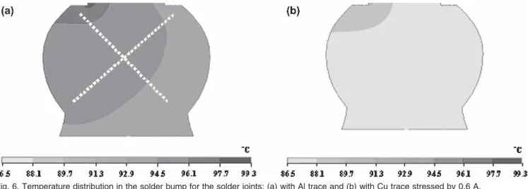
The Joule heating effect in the solder joints with the Cu traces was much smaller than that with the Al traces. Figure 5a and b show the temperature distributions in the stressing circuit for the solder joints with the Al traces and with the Cu traces, respectively, when stressed by 0.6 A. It is found that the maximum temperature in the Al was 148.8°C, whereas it decreased to 122.4°C in the Cu trace. In addition, the average temperature in the Al pads directly above the solder bumps was 97.4°C, yet it was reduced to 89.1°C when the Al traces were replaced by the Cu traces. The temperature distri-butions in the center cross section of the solder bumps were also inspected, as shown in Fig. 6a and b. Two temperatures, hot-spot and average, will be examined. Hot spots exist in the solder near the entrance points of the Al or Cu traces. For the solder joint with the Al traces, the hot-spot temperature was 99.3°C, whereas it was 90.6°C for the solder joint with the Cu traces. In this paper, the average temperature was obtained by averaging the temper-atures in the nodes on the white dotted lines in Fig. 6a. The average temperature in the solder bump with the Al traces was 96.7°C, and it deceased to 88.7°C for the solder joint with the Cu traces.
The temperature increase and hot-spot tempera-tures at various stressing currents were also inves-tigated. Figure 7a shows the average and hot-spot temperatures as a function of applied current for the two models. At lower stressing current, there was no obvious Joule heating effect, and thus there is no difference in hot-spot temperatures between the two models. However, the difference became larger at higher stressing currents. It could be as large as 59.9°C at 0.8 A. For the average temperature,
Fig. 3. Current-density distribution in the solder joint: (a) with Al trace and (b) with Cu trace.
Hsu, Yao, Liang, Chen, and Yeh 950
the trend is quite similar to that of the hot-spot temperature. At 0.8 A, the average solder temper-ature decreased from 58.6°C to 33.6°C when the Al trace was replaced by the Cu trace. These results indicate that the solder joint with the Cu trace would have lower Joule heating effect.
Owing to the hot spots, thermal gradients exist inside the solder joints. In this paper, the horizontal
thermal gradient is the difference between the tem-perature in the hot spot and the temtem-perature at the opposite end of the solder, divided by the diameter of the passivation opening. In addition, the vertical thermal gradient was obtained by subtracting the hot-spot temperature by the temperature in the sub-strate side, divided by the bump height. The results for thermal gradients are shown in Fig. 7b. The
Fig. 4. Current-density distribution in the solder layer along the bump-height direction: (a) top layer of solder with Al trace, (b) top layer of solder with Cu trace, (c) 20 mm below the UBM layer for the solder with Al trace, and (d) 20 mm below the UBM layer for the solder with Cu trace.
Fig. 5. Temperature distribution in the stressing circuit for the solder joints: (a) with Al trace and (b) with Cu trace stressed by 0.6 A. Temperature and Current-Density Distributions in Flip-Chip
solder joints with the Al traces have higher thermal gradients than those with the Cu traces. Both hor-izontal and vertical thermal gradients were less than 50°C/cm when the solder joints were stressed by 0.2 A or less. Nevertheless, the gradient in-creased rapidly as the applied current inin-creased. The horizontal thermal gradient may reach 964.9°C/cm when the solder joints with the Al traces are stressed by 0.8 A, and it decreased to 601.4°C/cm upon using the Cu traces. For both models, the hor-izontal thermal gradients were larger than the ver-tical ones under the same stressing conditions.
DISCUSSION Current Density Distribution
The Cu traces can relieve the current crowding effect in flip-chip solder joints. The mechanism may be explained as follows. Figure 8 shows the enlarged schematic for the solder joint near the pas-sivation opening. When the current approaches the passivation opening, some of the current may drift down to the solder bump through the passivation opening, and the rest of the current may continue
to drift to the right-hand side along the pad. When the lateral resistance, i.e., the resistance of the pad (Rpad), becomes smaller, more current will drift on the pad above the solder bump. In contrast, when the resistivity of the pad material increases, the Rpad also increases and more current drifts down to the substrate side, since the cross section of the solder bump was quite large compared with that of the pad. For the two models in this study, the bump resistance (Rbump) remains the same because the height of the bump and the cross section of solder are identical. When the Al trace/pad was replaced by the Cu trace/pad, the resistance of the pad (Rpad) became smaller. More current would drift along the Cu pad farther and then drift down toward the sub-strate side gradually. Therefore, for the solder joints with the Cu pad, less current would drift down toward the substrate at the entrance point of the Al trace into the solder bump, i.e., the crowding effect was relieved.
Temperature Distribution
The main reason for the lower Joule heating effect using the Cu traces is that the resistivity of Cu is
Fig. 7. (a) Average and hot-spot temperatures as a function of applied current for the two models. (b) Vertical and horizontal thermal gradients as a function of applied current for the two models.
Fig. 6. Temperature distribution in the solder bump for the solder joints: (a) with Al trace and (b) with Cu trace stressed by 0.6 A.
Hsu, Yao, Liang, Chen, and Yeh 952
about 63% that of Al. Furthermore, the major heat-ing source is the Al or Cu traces. In our simulation model, the total resistance for the stressing circuit was 1,120.7 mV, in which the resistance of the Al trace weighed 1,107.7 mV. Hence, the heat gener-ated from the two bumps and the Cu line in the substrate was much smaller compared with that of the Al or the Cu traces. When the Al trace was replaced by the Cu trace, the total resistance of the circuit was reduced to 710.4 mV. In general, the Joule heating power can be expressed as
P 5 I2R 5 j2rV (2)
where P is the Joule heating power, I is the current, R is the total resistance of the circuit, j is the cur-rent density, r is the electrical resistivity, and V is the volume. At a lower stressing current, the Joule heating effect was not serious, and the Si substrate is able to dissipate heat effectively. Although the Joule heating effect was still larger in the solder joint with the Al trace, there was no obvious differ-ence in temperature distribution in the two models at a lower stressing current. However, the differ-ence became more significant at a higher stressing current due to serious heat generation. Although the thermal conductivity of Cu is higher than that of Al, this is not the main reason that the solder joints with the Cu traces have a lower Joule heating effect. This is because the main path for heat dissi-pation is Si substrate. In our model, there was a 3-mm polyimide layer between the Al and the Cu metallization, which makes heat dissipation harder compared with real devices.
The occurrence of the hot spot may be attributed to two reasons. First, it was close to the heat source. It located near the entrance point of the Al or Cu trace, and the Al or Cu trace was the main heat source. Second, the local Joule heating may also contribute to the hot spot. As shown in Fig. 3, the
local current density in the hot spot was at least 10 times larger than the average value in the solder. Therefore, the hot spot occurred near the entrance point of the Al or Cu trace. The hot spot may be detrimental to the electromigration lifetime of the solder joints, since the diffusivity of the solder increases exponentially with the increase of the local temperature. The solder in the hot spot may be migrated away easier and voids may be formed after the depletion of the solder.
CONCLUSIONS
The temperature and current density distribu-tions in the solder joints with Al and Cu traces have been studied using finite-element analysis. It is found that the solder joints with the Cu trace have a lower temperature increase due to the Joule heat-ing effect, which was mainly due to its lower elec-trical resistivity. In addition, the Cu trace may alleviate the current crowding effect slightly. There-fore, the solder joints with the Cu trace are antici-pated to have longer electromigration lifetime than those with the Al trace at higher stressing current, primarily due to their lower Joule heating effect.
ACKNOWLEDGEMENT
The authors thank the National Science Council of the Republic of China for the financial support of this study through Grant No. 90-2216-E-009-042.
REFERENCES
1. International Technology Roadmap for Semiconductors (San Jose, CA: Assembly and Packaging Section, Semiconductor Industry Association, 2003), pp. 4–9.
2. K.N. Tu, J. Appl. Phys. 94, 5451 (2003).
3. S. Brandenburg and S. Yeh, Proc. Surface Mount Int. Conf. Exhib. (Edina, MN: SMTA, 1998), p. 337–344.
4. C.Y. Liu, C. Chen, C.N. Liao, and K.N. Tu, Appl. Phys. Lett. 75, 58 (1999).
5. H. Ye, C. Basaran, and D. Hopkins, Appl. Phys. Lett. 82, 7 (2003).
6. J.D. Wu, P.J. Zheng, K. Lee, C.T. Chiu, and J.J. Lee, Elec-tronic Components and Technology Conf. (Piscataway, NJ: IEEE, 2002), p. 452–457.
7. J.W. Nah, K.W. Paik, J.O. Suh, and K.N. Tu, J. Appl. Phys. 94, 7560 (2003).
8. J.R. Black, IEEE Trans. Electron Dev. ED-16, 338 (1969).
9. C. Everett, C. Yeh, W.J. Choi, and K.N. Tu, Appl. Phys. Lett. 80, 4 (2002).
10. T. L. Shao, S.W. Liang, T. C. Lin, and C. Chen, J. Appl. Phys., to be published (2005).
11. T.L. Shao, S.H. Chiu, C. Chen, D.J. Yao, and C.Y. Hsu, J. Electron. Mater. 33, 1350 (2004).
12. R. Tummala, Fundamentals of Microsystem Packaging (New York: McGraw-Hill, 2001), p. 225.
Fig. 8. Enlarged schematic for the solder joint near the passivation opening, showing the two paths for electron flow when the current entered the passivation opening.
Temperature and Current-Density Distributions in Flip-Chip