488 IEEE PHOTONICS TECHNOLOGY LETTERS, VOL. 24, NO. 6, MARCH 15, 2012
Optical Simulation and Fabrication of
Near-Ultraviolet LEDs on a Roughened Backside
GaN Substrate
Yi-Keng Fu, Yu-Hsuan Lu, Rong Xuan, Chia-Hsin Chao, Yan-Kuin Su, and Jenn-Fang Chen
Abstract— In this letter, the numerical and experimental demonstrations for enhancement of light extraction efficiency in near-ultraviolet light-emitting diodes (LEDs) with a roughened backside on the N-face surface of GaN substrate through a chem-ical wet-etching process are investigated. It was also found that the increased etching time can increase the height of hexagonal pyramids and decrease the density of hexagonal pyramids. With 20-mA injection current, it was found that forward voltages were 3.13 and 3.16 V while output powers were 13.15 and 27.18 mW for the conventional LED and roughened backside LED, respectively. Index Terms— Chemical wet-etching, GaN, light extraction, near-ultraviolet light-emitting diode (NUV LED), simulation.
I. INTRODUCTION
L
ARGE area substrates for homoepitaxial growth of GaN layers have recently become available as a result of recent progress in production of thick freestanding GaN (FS-GaN) layers grown by hydride vapor phase epitaxy (HVPE) [1]. Such substrates have been successfully applied to grow LED structures using metal organic chemical vapor deposition (MOCVD) [2], resulting in high quality films, as demonstrated by their superior optical and electrical characteristics. Very recently, Chao et. al. have been reported the LED grown on GaN substrate can be obtained a higher light-output power and lower efficiency droop, compared with the LED grown on sapphire [3]. To realize solid-state lighting, however, one needs to further improve output efficiency of these LEDs. It is known that light-extraction efficiency of GaN-based LED is limited mainly by the large difference in refractive index between GaN film and the surrounding air. The critical angle for photons to escape from GaN film is determined by Snell’s law. The angle is crucially important for the light-extraction efficiency of LEDs. Since the refractive indexes of GaN and air are 2.5 and 1, respectively, external quantum efficiency was limited Manuscript received September 26, 2011; revised December 23, 2011; accepted December 30, 2011. Date of publication January 3, 2012; date of current version February 29, 2012.Y.-K. Fu, R. Xuan, and C.-H. Chao are with the Department of Opto-Electronics Epitaxy and Devices, Industrial Technology Research Insti-tute, Hsinchu 31040, Taiwan (e-mail: [email protected]; [email protected]; [email protected]).
Y.-H. Lu and Y.-K. Su are with the Department of Electrical Engineering, Institute of Microelectronics, National Cheng-Kung University, Tainan 70101, Taiwan (e-mail: [email protected]; [email protected]).
J.-F. Chen is with the Department of Electrophysics, National Chiao Tung University, Hsinchu 30050, Taiwan (e-mail: [email protected]).
Color versions of one or more of the figures in this letter are available online at http://ieeexplore.ieee.org.
Digital Object Identifier 10.1109/LPT.2011.2182606
to only a few percents for conventional GaN-based LEDs. It has been demonstrated that several methods can be used to improve light-extraction efficiency in InGaN-based LEDs on Al2O3substrate, such as bottom patterned Al2O3substrate [4], top p-type GaN:Mg rough surface processes [5], the formation of photonic crystal structure [6] and selective oxidization on the mesa sidewall through a photoelectrochemical (PEC) wet oxidation process [7]. Among these, PEC etching has advantages in terms of the compatibility with conventional semiconductor processing equipment and easy scalability to large wafers as well as the processing cost.
Very recently, we have been published the roughened back-side structure (RBs) could mainly enhance the light extrac-tion efficiency, especially for near-ultraviolet (n-UV) [8]. The Larger improvement for n-UV LEDs is attributed to the dif-ferent transmittance as a function of wavelength by hexagonal pyramids after chemical wet-etching process, compared with blue LEDs. In this study, the effect of RBs on optoelec-tronic characteristics of n-UV LEDs was further investigated. Detailed fabrication process, numerical demonstrations, and the properties of fabricated LEDs will also be discussed.
II. EXPERIMENT
The n-UV InGaN/GaN LEDs used in this study were all grown on c-face (0001) 2-inch GaN substrates in a SR-4000 atmospheric pressure metalorganic chemical vapor deposition system. GaN substrates were fabricated by C. L. Chao. et. al. group [3]. LED structure consists of a 4-μm-thick Si-doped GaN n-cladding layer, an multi quantum well (MQW) active layer, a 20-nm-thick p-type Mg-doped Al0.2Ga0.8N layer and a 200-nm-thick Mg-doped GaN layer. The MQW active region consists of five periods of 2.4-nm-thick undoped InxGayN well layer and 9-nm-thick undoped GaN barrier layer. For the fabrication of LEDs, indium tin oxide (ITO) was first deposited on these LEDs as a transparent contact layer (TCL). Then, we partially etched the surface of the samples until the n-type GaN layers were exposed. We subsequently deposited Cr/Au onto the exposed n-type and p-type GaN layer to serve as the n-type and p-type electrode. The chip size of LEDs was 375μm × 375 μm.
After chip processes, the epitaxial wafers were then lapped down to about 110μm. We subsequently placed these samples into a hot 2-M KOH solution without any stirring to form in the pyramidal structure at the N-face GaN substrate. During wet-etching process, we used various etching time at 80 °C 1041–1135/$31.00 © 2012 IEEE
FU et al.: OPTICAL SIMULATION AND FABRICATION OF NEAR-ULTRAVIOLET LEDs 489
Fig. 1. 30° tile-view and cross-sectional (inset) SEM images of the surface morphology on N-face GaN substrate at 80 °C in various times of KOH solutions (a) before etching, (b) 1 min, (c) 5 min, (d) 10 min, (e) 30 min, and (f) 60 min.
in order. We then used scribe and break to complete the fabrication of LEDs. Detail of the schematic of the LED structure and the process steps can be found elsewhere [8]. The LED device that was fabricated through this process flow without and with a chemical wet-etching process was defined as a standard LED (LEDI), and a roughened backside structure (RBs) LED with various etching times 1 min: LEDII, 10 min: LEDIII and 30 min: LEDIV. The geometric morphology of these LED structures was observed through a scanning electron microscopy (SEM). These chips were p-sideup-mounted on a Ag TO-46 and molded in epoxy resin. We measured their room temperature (RT) current-voltage (I-V) characteristics by an HP4156 semiconductor parameter analyzer. Light output power-current (L-I) characteristics of these fabricated LEDs were also measured using the molded LEDs with the integrated sphere detector. To minimize heating effect, the injection current was a pulsed current source with 1 % duty cycle and 10 kHz frequency.
III. RESULTS ANDDISCUSSION
In order to understand the wet-etching process of the RB-LED, we also prepared the GaN substrate samples with various wet-etching times after lapping down to about 110 μm. Fig-ure 1 shows the 30° tile-view and cross-sectional (inset) SEM images of the surface morphology on N-face GaN substrate at 80 °C in various times of KOH solutions (a) before etching: sample I, (b) 1 min: sample II, (c) 5 min: sample III, (d) 10 min: sample IV, (e) 30min: sample V and (f) 60 min: sample VI. It was found that pyramidal structure was observed with chemical etching solution of N-face GaN. It was also found that the increased etching time can increase the height of hexagonal pyramids and decrease the density of hexagonal pyramids. Previously reported chemical etching solution such as KOH, Sulfuric Acid (H2SO4) and PEC was found to selec-tively etch the N-face GaN but not the Ga-face GaN [9, 10]. Li et. al. reported the etch reaction under similar conditions as 2Ga N +3H2O K O H−→ Ga2O3+2N H3 where KOH is both a catalyst for the reaction and a solvent for the resulting Ga2O3 [11]. Because the wet-etching process occurs through the negatively charged OH−ions, Ga-face GaN is more stable than N-face GaN due to the negatively charged triple dangling bonds at the surface of Ga-polar GaN [9, 11]. In this study, the N-face GaN was exposed at the bottom of the GaN substrate. As a result, hexagonal pyramid will be formed at the bottom of the chip. The etch process constantly reacted by increasing the etching time by exposing more OH− ions. It was also
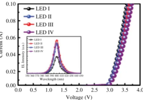
0.0 0.00 0.02 0.04 0.06 0.08 0.10 LED I LED II LED III LED IV LED I LED II LED III LED IV 0.5 350 360 370 380 380 390 Wavelength (nm) EL Intensit y (a. u .) 400 410 420 430 440 450 1.0 1.5 2.0 Voltage (V) C u rrent (A) 2.5 3.0 3.5 4.0
Fig. 2. I–V characteristics of these four LEDs are measured at a 20-mA injection current. The inset of Fig. 2 shows the EL wavelength of these four LEDs at a 20-mA injection current.
0.00 0.02 0.12 0.00 0.02 0.04 0.06 0.08 0.10 0.04 Current (A) LED I LED II LED III LED IV O u tp u t po w er ( W ) 0.06 0.08 0.10
Fig. 3. I–V characteristics of these four LEDs are measured at a 20-mA injection current. The inset of Fig. 2 shows the EL wavelength of these four LEDs at a 20-mA injection current.
found that the etching process ended in six {1011} faces of the GaN layer. These results agree well with that reported by Ng et. al. [9].
Figure 2 shows I-V characteristics of these fabricated LEDs. It was found that 20 mA forward voltages of these LEDs were 3.14, 3.16, 3.20 and 3.21 V for the LEDI, II, III and IV, respectively. The slightly larger forward voltage observed from roughened backside LED is probably related to wet-etching-induced damages. The inset of Fig. 2 shows the electroluminescence (EL) wavelength of these four LEDs at a 20mA injection current. It was found that EL peak positions of these four LEDs all around at 405 nm with the same full-width-half-maximum (FWHM) of 11 nm. It was also found that EL intensities of the LEDs with chemical wet etching were larger than the conventional LEDs without chemical wet etching. This can be attributed to the better light-extraction efficiency for the LEDs with RBs.
Figure 3 shows L-I characteristics of these four LEDs. It was also found that output power of LED with RBs was always larger than that of LEDI. With 20 mA injection current, it was found that the output powers of these LEDs were 13.15, 27.18, 25.56 and 22.67 mW for the LEDI, LEDII, LEDIII and LEDIV, respectively. Compared with LEDI, we can enhance the output power by 107%, 94% and 72% for LEDII, LEDIII and LEDIV by using the RBs LED, respectively. The large enhancement can also be attributed to the better light-extraction efficiency for the LEDs with RBs. As a result, the smaller vertical length and higher density of hexagonal pyramids are beneficial to the improvement of light extraction efficiency. Figure 4 shows the simulation result proposed LED with RBs similar to the etching profile of Fig 1 can be used to explain such an enhancement.
490 IEEE PHOTONICS TECHNOLOGY LETTERS, VOL. 24, NO. 6, MARCH 15, 2012
P
hoto intensit
y
Fig. 4. Simulation results of proposed LEDs. (a) LEDII: KOH etching time= 1 min. (b) LEDIII: KOW etching time= 10 min. (c) LEDIV: KOW etching time= 30 min. 0.00 100 90 60 30 0 30 −90 −60 −30 80 60 40 20 0 Degree (a) (b) LED I LED II LED III LED IV LED I LED II LED III LED IV Intensit y (a. u .) −20 −40 −60 −80 −100 0.02 0.04 0.06 0.08 0.10 0.2 0.0 0.4 0.6 0.8 1.0 0.12 0.14
Fig. 5. LED samples show measurements of (a) far-field radiation patterns and (b) normalized output beam patterns at a 20-mA injection current.
The finite-difference time-domain (FDTD) analysis [12] is used to study the irradiance behavior of the proposed LED with random IPSs. In order to describe the random propagation of unpolarized photons trapped within or escaping from LEDs, multiple TE- and TM-polarized point sources with the wavelength of 405 nm are arranged within the MQWs region with an interval of 100 nm. The structure parameters given in the numerical analysis include p-GaN layer thickness hpGa N = 0.2 μm, MQWs thickness hM Q W s = 0.012 μm, n-GaN layer thickness hnGa N = 4 μm, GaN substrate thickness
hGa N substrat e= 100 μm, p-GaN reflective index npGa N = 2.5, MQWs reflective index nM Q W s= 2.55, n-GaN reflective index
nnGa N = 2.5, GaN substrate reflective index nGa N substrat e= 2.5, RBs slanted angle θ = 58°, and the RBs etching pro-file is similar to the Figure 1. To facilitate the numerical simulation, a spatial discretization of 20 μm × 40 μm in the computation window is employed under the limitation of computer memory. In order to explain the effect of RBs on improving the light extraction efficiency of LEDs, three different types of LEDs are simulated and demonstrated in Fig. 4(a)–(c). In this simulation, the same amount of point sources is arranged in the MQWs region. As can be found in this figure, the smaller vertical length and higher density of hexagonal pyramids are beneficial to the improvement of light extraction efficiency. The most light can be extracted from GaN substrate to air through RBs of LEDII. When we increased the etching time, the height of hexagonal pyramids was increased and the density of hexagonal pyramids was decreased. The light emitted from the MQWs is more difficult to extract to the air, compared with LEDII. In other words, the light passes through the smaller vertical length and higher density of hexagonal pyramids can be extracted effectively. Therefore, the output power can be improved by using RBs because the most light cam escape from the GaN substrate. These results are consistent with the Fig. 3.
Figure 5 (a) shows the far-filed radiation patterns of these four LEDs at a 20 mA injection current and Fig. 5 (b) shows
the normalized output beam patterns of these four LEDs at a 20 mA injection current. The angles of output beam pattern are almost the same. A comparison with the LEDI indicates clearly that the intensity of output beam pattern of LED with RBs is higher. The RBs are beneficial to most light escape from the GaN substrate. These results agree with the assertion shown in Fig. 4.
IV. CONCLUSION
In summary, nitride-based LEDs with a roughened backside GaN substrate were proposed and fabricated. By chemical wet-etching process, the hexagonal pyramids can be formed in the N-face GaN substrate. It was found that the increased etching time can increase the height of hexagonal pyramids and decrease the density of hexagonal pyramids. It was also found that such RBs could mainly enhance the light extraction efficiency. Compared with LEDI without chemical wet etching, it was found that we can enhance the 20 mA output power by 107 % from the LEDII with RBs. The simulation successfully explains the enhancement of light extraction efficiency in LEDs with RBs.
REFERENCES
[1] M. K. Kelly, R. P. Vaudo, V. M. Phanse, L. Görgens, O. Ambacher, and M. Stutzmann, “Large free-standing GaN substrates by hydride vapor phase epitaxy and laser-induced liftoff,” Jpn. J. Appl. Phys., vol. 38, no. 3A, pp. L217–L219, 1999.
[2] C. R. Miskys, M. K. Kelly, O. Ambacher, G. Martínez-Criado, and M. Stutzmann, “GaN homoepitaxy by metalorganic chemical-vapor deposition on free-standing GaN substrates,” Appl. Phys. Lett., vol. 77, no. 12, pp. 1858–1860, Sep. 2000.
[3] C. L. Chao, et al., “Freestanding high quality GaN substrate by associated GaN nanorods self-separated hydride vapor-phase epitaxy,” Appl. Phys. Lett., vol. 95, no. 5, pp. 051905-1–051905-3, Aug. 2009.
[4] M. Yamada, et al., “InGaN-based near-ultraviolet and blue-light-emitting diodes with high external quantum efficiency using a patterned sapphire substrate and a mesh electrode,” Jpn. J. Appl. Phys., vol. 41, no. 12B, pp. L1431–L1433, Dec. 2002.
[5] C. H. Kuo, et al., “Nitride-based light-emitting diodes with p-AlInGaN surface layers,” IEEE Electron Device Lett., vol. 52, no. 10, pp. 2346– 2349, Oct. 2005.
[6] A. David, et al., “Photonic-crystal GaN light-emitting diodes with tailored guided modes distribution,” Appl. Phys. Lett., vol. 88, no. 6, pp. 061124–061126, Feb. 2006.
[7] C. F. Lin, Z. J. Yang, J. H. Zheng, and J. J. Dai, “Enhanced light output in nitride-based light-emitting diodes by roughening the mesa sidewall,” IEEE Photon. Technol. Lett., vol. 17, no. 10, pp. 2038–2040, Oct. 2005.
[8] Y. K. Fu, et al., “Study of InGaN-based light-emitting diodes on a roughened backside GaN substrate by a chemical wet-etching process,” IEEE Photon. Technol. Lett., vol. 23, no. 19, pp. 1373–1375, Oct. 1, 2011.
[9] H. N. Ng, N. G. Weimann, and A. Chowdhury, “GaN nanotip pyramids formed by anisotropic etching,” J. Appl. Phys., vol. 94, no. 1, pp. 650– 653, Jul. 2003.
[10] Y. Gao, M. D. Craven, J. S. Speck, S. P. DenBaars, and E. L. Hu, “Dislocation- and crystallographic-dependent photoelectrochemical wet etching of gallium nitride,” Appl. Phys. Lett., vol. 84, no. 17, pp. 3322– 3324, Apr. 2004.
[11] D. Li, et al., “Selective etching of GaN polar surface in potas-sium hydroxide solution studied by X-ray photoelectron spec-troscopy,” J. Appl. Phys., vol. 90, no. 8, pp. 4219–4223, Oct. 2001.
[12] A. Taflove, Computational Electrodynamics: The Finite-Difference Time Domain Method, 2nd ed. Norwood, MA: Artech House, 2000, ch. 7, pp. 285–347.