Cu(In,Ga)Se2 thin films preparation from CuGa-In metallic alloy and
Se thin film by atmosphere pressure plasma deposition system
Kow-Ming Changa,b, Po-Ching Hoa, Kuo-Hui Yangc, Shen-Bin Wuc, Chi-Hung Liuc
a
Department of Electronics Engineering & Institute of Electronics, National Chiao Tung University, 1001 Ta Hsueh Road, Hsinchu, Taiwan 30010, R.O.C.
b
College of Electrical and Information Engineering, I-Shou University, No.1, Sec. 1, Syuecheng Rd., Dashu Township, Kaohsiung County, Taiwan 84001, R.O.C.
c
Industrial Technology Research Institute, Mechanical and Systems Research Laboratories, Hsinchu, Taiwan 310, R.O.C.
An atmosphere pressure plasma (APP) deposition system with dielectric barrier discharge (DBD) is proposed for deposition selenium thin films on CuGa-In metallic precursors and transformed into Cu(In,Ga)Se2 (CIGS) thin films by rapid thermal
process (RTP). Morphologies and thicknesses of selenium thin films deposited on In/CuGa/Mo/SLG can be affected by plasma power which also has impact on crystallinity of CIGS absorber. With the increase in plasma power, CIGS grains tend to distribute non-uniformly. Plasma power of 100W has the smallest FWHM of the main peak (112). Insufficient selenium incorporation into precursors result in undesired phases such as Cu3Se2, Cu2Se and
separation phase, CuGaSe2 compound. Compositions of optimal
selenized CIGS thin film deposited by scanning 180times are Cu/(In+Ga) = 1.03 and Ga/(In+Ga) = 0.24.
Introduction
Chalcopyrite-structure Cu(In,Ga)Se2 (CIGS), which has high optical absorption
coefficient, is one of the most promising light-absorbing materials for high conversion efficiency and low cost thin film solar cells (1,2). The major processing techniques for CIGS thin films deposition are co-evaporation and selenization. The process of rapid thermal selenization is deposition of selenium thin films on CuGa-In metallic alloy and then incorporation of selenium into the precursors by rapid thermal process (RTP) (3-5). RTP is believed to reduce the loss of In2Se (6). The conventional selenium thin films
were obtained by vacuum evaporation. However, drawbacks of vacuum process include the demands of high vacuum pumping system and difficulty in roll-to-roll process. In this study, an atmosphere pressure plasma (APP) deposition system with dielectric barrier discharge (DBD) is proposed for deposition selenium thin films on In/CuGa/Mo/SLG. Many advantages of the APP deposition system (7,8) are low equipment cost, high processing speed and application in roll-to-roll process and large area deposition.
Experimental
About 700nm thick CIG layers were deposited on the Mo-coated soda lime glass by DC-magnetron sputtering. The chemical compositions of the metallic precursors were 52.50 at% Cu, 32.40 at% In and 15.10 at% Ga, confirmed by EDS. Selenium thin films were deposited on In/Cu0.8Ga0.2/Mo/SLG substrates at room temperature using APP
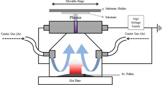
deposition system. As shown in Fig. 1, the APP deposition system consists of a linear plasma source, hot plate, quartz container and movable substrate holder. Selenium pellets were used as an evaporation source located onto the bottom of quartz container and heated up by hot plate at 400oC. Evaporated selenium vapor was carried through plasma discharging area by argon carrier gas. The argon flow rate is 30SLM and gap between substrate and plasma source is 5mm. For the duration of deposition, scan speed was 10mm/s. In order to investigate the influence of plasma power on as-deposited selenium thin films and selenized thin films, plasma power was varied as 0, 50 and 100W. Moreover, scanning times of deposition was varied as 120 and 180times due to adjustment thicknesses of selenium thin films and obtaining the best quality of CIGS films. Selenization process was carried out by one-step RTP. The maximum temperature reached during RTP was about 550oC and the ramp rate was about 1oC/s. The surface morphologies and composition of selenium and selenized thin films were analyzed by a Hitachi S-4700I scanning electron microscope (SEM) and energy dispersive spectrometer (EDS), respectively. The roughness was determined by a DI Digital DI-D3000 atomic force microscopy (AFM). X-ray diffraction (XRD) patterns of the selenized CIGS films were measured using PANalytical X'Pert x-ray diffractometer.
Figure 1. Schematic diagram of the atmosphere pressure plasma deposition system.
Results and Discussion
Plasma power effect
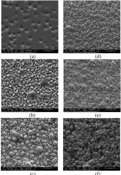
Figure 2a-c shows surface SEM images of as-deposited selenium thin films of different plasma power, 0, 50, 100W. As power increases, the formed selenium thin films tend to aggregate into small atomic group due to gaining of kinetic energy from plasma. The substrate temperature was elevated by increasing plasma power and scanning times, as shown in Fig. 3. The plasma power of 100W has the highest heating rate of substrate. There is no obvious difference in heating rates of 0W and 50W. Large hills among surfaces of selenium thin films were observed, as shown in Figs. 2b and c. EDS spot analyses on these large hills shows that they are indium. Data in Table I presents thicknesses, deposition rates and RMS values of the selenium thin films prepared by different plasma power and RMS values of selenized thin films. Thicknesses of selenium thin films decrease as plasma power increase. This result can be explained by
re-evaporation of absorbed selenium atoms (9) due to high substrate temperature resulted from higher plasma deposition power. Figure 2d-f shows selenized CIGS thin films prepared from stacked In/CuGa metallic precursors and selenium thin films scanned 120 times for different plasma power, 0, 50 and 100W. As power increases, the RMS values of selenized thin films increases. A possible explanation for this is that rougher morphologies of selenium thin films caused non-uniform selenium diffusion into precursor layers during RTP. EDS analysis of selenized CIGS thin fims shows a decrease in selenium atomic ratio from 45.3 at% to 32.0 at% when plasma power increased. The data are consistent with area of as-grown selenium thin films covered on metallic precursor layers, as shown in Figs. 2a-c. The EDS results show that plasma power increased with decreasing Ga/(In+Ga) atomic ratios from 0.33 to 0.29. AFM images of selenized CIGS thin films prepared from In/CuGa metallic alloy and selenium thin films of plasma power, 0 , 50 and 100W, as shown in Fig.4. With the increase in plasma power, the surface roughness increases and grains tend to distribute non-uniformly. The values are given in Table I.
(a) (d) (b) (e) (c) (f)
Figure 2. Surface SEM images of as-deposited selenium thin films for different plasma power: (a)0W (b)50W (c)100W, and selenized CIGS thin films prepared from In/CuGa metallic alloy and selenium thin films scanned 120times for different plasma power: (d)0W (e)50W (f)100W.
Table I. Thicknesses, deposition rates and RMS values (Before RTP) of selenium thin films scanned 120times for different plasma power and RMS values (After RTP) of selenized CIGS films.
Plasma power Thickness Deposition rate RMS
(W) (nm) (nm/scan one time) (nm)
Before RTP After RTP
0 1142.8 9.52 17.50 189.91
50 1007.0 8.39 300.89 273.16
100 766.8 6.39 236.52 348.42
Figure 3. Elevated substrate temperature for different plasma power and scanning times.
(a) (b) (c)
Figure 4. AFM images of selenized CIGS thin films prepared from In/CuGa metallic alloy and selenium thin films of plasma power: (a)0W (b)50W (c)100W.
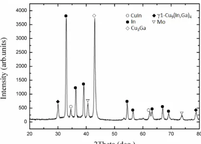
Figure 5 shows GIXRD spectrum of as-deposited CuGa/In precursor alloy by sputtering. Cu3Ga and In were two strongest peaks observed in the spectrum. γ1 phase,
which is believed to be a Cu9In4–Cu9Ga4 alloy (10,11) , existed after precursor annealing.
Figure 6a dipics GIXRD spectrum of selenium thin films, which was scanned 120times , deposited on In/CuGa/Mo/SLG for different plasma power, 0, 50 and 100W. As plasma power increased from 0 to 100W, intensity of CuIn and Cu3Ga phases increased due to
improving crystallinity. It is interesting to note that intensity of CuIn phases exhibited greater variation than intensity of Cu3Ga phases, a possible explanation for this might be
that difference in diffusion coefficient between In and Ga (12). According to EDS analysis, indium contents increased more rapidly than gallium contents, which cause decrease in Ga/(In+Ga) ratio and increase in the lattice constant. In addition, amorphous selenium was transformed into trigonal selenium because of elevating substrate temperature above 105oC (13) by high plasma power. As shown in Fig. 6b, all selenized CIGS thin films exhibit preferred orientation along (112) plane. Se-poor compounds such as Cu2Se, Cu3Se2 and InSe phases were observed in the selenized CIGS thin films due to
thinner selenium films, which cause insufficient selenium supply during RTP. It is noteworthy that weakended CuGaSe2 peaks near CIGS main peaks appeared because of
non-uniform distribution of In and Ga (14).
Figure 5. GIXRD spectrum of the CuGa-In precursor alloy deposited on Mo/SLG by sputtering.
(a) (b)
Figure 6. GIXRD spectrum of (a)Selenium thin films scanned 120times deposited on In/CuGa/Mo/SLG for different plasma power (b)Selenized thin films prepared from In/CuGa metallic alloy and selenium thin films of different plasma power.
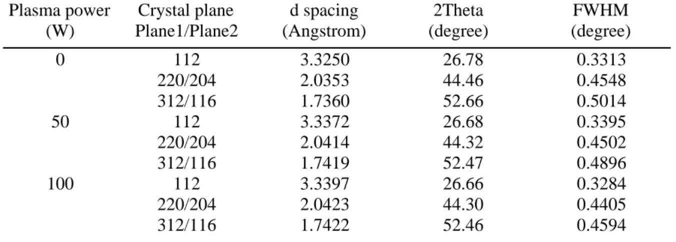
Full width at half maximum (FWHM), 2Theta (peak’s degree) and d spacing of different (hkl) for CIGS are given in Table II. As mentioned earlier, plasma power increases with increasing the lattice constant. There was a positive correlation between d spacing and the lattice constant. The negative shift in 2theta values of (112), (220/204) and (312/116) peaks for CIGS thin films resulted from increment of d spacing. The selenized CIGS thin film prepared from In/CuGa metallic alloy and selenium thin film of plasma power, 100W, has the smallest FWHM of (112), (220/204) and (312/116) peaks.
Table II. Crystalline properties of selenized CIGS thin films prepared from In/CuGa metallic alloy and selenium thin films of different plasma power.
Plasma power Crystal plane d spacing 2Theta FWHM
(W) Plane1/Plane2 (Angstrom) (degree) (degree)
0 112 3.3250 26.78 0.3313 220/204 2.0353 44.46 0.4548 312/116 1.7360 52.66 0.5014 50 112 3.3372 26.68 0.3395 220/204 2.0414 44.32 0.4502 312/116 1.7419 52.47 0.4896 100 112 3.3397 26.66 0.3284 220/204 2.0423 44.30 0.4405 312/116 1.7422 52.46 0.4594
Changing scanning times
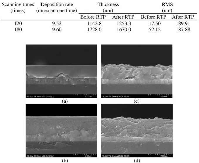
Figure 7a and b shows cross-sectional SEM images of selenium thin films deposited on In/CuGa/Mo/SLG without plasma power for different scanning times, 120 and 180times. Thicknesses, deposition rates and RMS values of as-deposited selenium thin films prepared by APP system for different scanning times and RMS values of selenized CIGS films are summarized in Table III. Data in Table III shows that thicknesses and RMS values of as-deposited selenium thin films scanned 180times is higher than one scanned 120times, but RMS values of selenized CIGS films are almost the same. Figure 7c and d presents selenized CIGS thin films prepared from In/CuGa metallic alloy and selenium thin films deposited without plasma power for different scanning times, 120 and 180times. The results indicate that the CIGS film is thicker and with better adhesion when selenized films prepared from In/CuGa metallic alloy with 180 times than one with 120 scanning times. Table IV compares EDS results for atomic composition of the selenized CIGS thin films prepared from metallic In/CuGa alloy and selenium thin films scanned 120 and 180times. Typical compositions of selenized CIGS thin film deposited by scanning 180times are Cu/(In+Ga) = 1.03 and Ga/(In+Ga) = 0.24. For selenium deposited with 120times, the CIGS thin film shows that the Se/Cu atomic ratio is below 2 due to insufficient selenium deposition. Moreover, the case of 180times also reveals the slightly selenium deficiency. The above result can be attributed by elevating substrate temperature during selenium deposition, which results in partly transformation of amorphous selenium to crystallized selenium, as shown in Fig. 8a. As compared with the amorphous selenium, crystallized selenium has lower self-diffusion coefficient and longer reaction time with metallic In/CuGa precursors during RTP.Figure 8a shows GIXRD spectrum of selenium thin films deposited on In/CuGa/Mo/SLG
without plasma and scanned 120 and 180times. Both as-grown selenium thin films are comprised of multiple phases: CuIn, Cu3Ga, In and Se. Selenium deposited without
plasma power are almost amorphous thin films. Figure 8b dipics GIXRD spectrum of selenized CIGS thin films prepared from In/CuGa metallic alloy and selenium thin films deposited for different scanning times. The result indicates that the selenized CIGS thin film prepared from stacked metallic alloy and selenium thin film scanned 180times is without any undesired phases such as Cu3Se2,Cu2Se and CuGaSe2. Crystalline properties
of selenized CIGS thin films are summarized in Table V. Compared to other selenized films, the crytallinity condition of CIGS thin film prepared from In/CuGa metallic alloy with 180 selenium deposition scanning times is most ideal.
Table III. Thicknesses, deposition rates and RMS values (Before RTP) of selenium thin films prepared by APP system for different scanning times and RMS values (After RTP) of selenized CIGS films.
Scanning times (times)
Deposition rate Thickness RMS
(nm/scan one time) (nm) (nm)
Before RTP After RTP Before RTP After RTP
120 9.52 1142.8 1253.3 17.50 189.91 180 9.60 1728.0 1670.0 52.12 187.88 (a) (c) (b) (d)
Figure 7. Cross-sectional SEM images of as-deposited selenium thin films for different scanning times: (a)120times (b)180times ,and selenized CIGS thin films prepared from In/CuGa metallic alloy and selenium thin films deposited without plasma power for different scanning times: (c)120times (d)180times.
Table IV. EDS results for atomic composition of the selenized thin films prepared from metallic CIG alloy and selenium thin films deposited for different scanning times.
Scanning times Element concentration (at%) Cu/(In+Ga) Ga/(In+Ga)
(times) Cu In Ga Se
120 31.64 14.82 7.24 46.30 1.43 0.33
180 26.00 19.19 6.01 48.80 1.03 0.24
(a) (b)
Figure 8. GIXRD spectrum of (a)Selenium thin films deposited on In/CuGa/Mo/SLG without plasma for different scanning times (b)Selenized CIGS thin films prepared from In/CuGa metallic alloy and selenium thin films deposited for different scanning times.
Table V. Crystalline properties of selenized CIGS thin films prepared from In/CuGa metallic alloy and selenium thin films deposited for different scanning times.
Scanning times Crystal plane d spacing 2Theta FWHM
Plane1/Plane2 (Angstrom) (degree) (degree)
120 112 3.3250 26.78 0.3420 220/204 2.0353 44.46 0.4548 312/116 1.7360 52.66 0.5014 180 112 3.3203 26.87 0.3084 220/204 2.0297 44.59 0.4146 312/116 1.7311 52.82 0.5140 Conclusion
In conclusion, selenium thin films deposited by APP deposition system successfully reacted with metallic precursors using RTP and formed a good quality of CIGS absorber. As plasma power increases, thicknesses of selenium thin films deposited on In/CuGa/Mo/SLG decrease owing to re-evaporation of selenium caused by elevating substrate temperature. With the increase in plasma power, the surface roughness increase and grains tend to distribute non-uniformly. Plasma power of 100W has the smallest FWHM of (112), (220/204) and (312/116) peaks. Insufficient selenium incorporation into precursors result in undesired phases such as Cu3Se2,Cu2Se and phase separation
compound CuGaSe2. Compositions of optimal selenized CIGS thin film deposited by
scanning 180 times are Cu/(In+Ga) = 1.03 and Ga/(In+Ga) = 0.24. In the case of 180times, it shows that the Se/Cu atomic ratio is slightly below 2. This result can be attributed by elevating substrate temperature during selenium deposition, which results in partly transformation of amorphous selenium to crystallized selenium. The crystallized selenium has lower self-diffusion coefficient and longer reaction time with metallic In/CuGa precursors during RTP. A reasonable approach to tackle this issue could be to use water flowed through the bottom of substrate to force evaporative cooling.
Acknowledgments
The authors are grateful for the support of this research by the Mechanical and Systems Research Laboratories, Industrial Technology Research Institute (ITRI).
References
1. M. Kawamura, T. Fujita, A. Yamada, M. Konagai, J. Cryst. Growth, 311, 753 (2009). 2. K. H. Kim, K. H. Yoon, J. H. Yun, B. T. Ahn, Electrochem. Solid-State Lett., 9, A382
(2006)
3. S. S. Kulkarni, G. T. Koishiyev, H. Moutinho, N. G. Dhere, Thin Solid Films, 517, 2121 (2009).
4. H. Park, S. C. Kim, S. H. Lee, J. Koo, S. H. Lee, C. W. Jeon, S. Yoon, W. K. Kim,
Thin Solid Films, 519, 7245 (2011).
5. V. Probst, W. Stetter, W. Riedl, H. Vogt, M. Wendl, H. Calwer, S. Zweigart, K. D. Ufert, B. Freienstein, H. Cerva, F. H. Karg, Thin Solid Films, 387, 262 (2001)
6. S. J. Ahn, C. W. Kim, J. H. Yun, J. C. Lee, K. H. Yoon, Sol. Energy Mater. Sol. Cells,
91,1836 (2007)
7. S. H. Yang, C. H. Liu, C. H. Su, H. Chen, Thin Solid Films, 517,5284 (2009)
8. K. M. Chang, S. H. Huang, C. J. Wu, W. L. Lin, W. C. Chen, C.W. Chi, J.W. Lin, C. C. Chang, Thin Solid Films, 519,5114 (2011)
9. M. Ozenbas, J. Mater. Sci., 22, 1419 (1987).
10. G. M. Hanket, W. N. Shafarman, B. E. McCandless, R. W. Birkmire, Journal of
Applied Physics, 102, 074922 (2007)
11. R. Kamada, W. N. Shafarman, R. W. Birkmire, in Proceedings of 33rd IEEE
Photovoltaic Specialists Conference, San Diego, CA, IEEE (2008).
12. M. Marudachalam, R. W. Birkmire, H. Hichri, J. M. Schultz, A. Swartzlander, M. M. Al-Jassim, Journal of Applied Physics, 82, 2896 (1997)
13. E. Chatterjee, S. P. Sen Gupta, Journal of materials science latters, 5, 119 (1986) 14. C. M. Xu, Y. Sun, L. Zhou, F.Y. Li, L. Zhang, Y. M. Xue, Z. Q. Zhou, Q. He, China