增進複晶矽薄膜電晶體特性之先進技術
77
0
0
全文
(2) 增進複晶矽薄膜電晶體特性 之先進技術. 研究生:蕭逸璿. 指導教授:崔秉鉞. 國立交通大學 電子研究所碩士班. 摘要. 本論文分為兩個部分。第一個部分,將修正蕭特基阻障鰭狀電晶體 (Modified-Schottky-Barrier FinFET, MSB FinFET)的概念延伸應用到修正 蕭特基阻障薄膜電晶體(MSB TFT)。第二個部分則探討將二氧化鉿做為薄膜電晶 體時,閘極區域之外的二氧化鉿的去除技術。 在經過離子植入矽化物及其後的活化製程後,可以形成超淺源極/汲極延伸 (S/D extension)以調變蕭特基阻障性質。此超淺源極/汲極延伸可以降低傳統蕭 特基接面漏電。此超淺源極/汲極延伸可連接通道以及源極/汲極金屬矽化物,使 得修正蕭特基阻障薄膜電晶體可以維持較低的源極注入阻抗而得到較高的導通 電流。在元件導通模式下,較高的導通電流是由矽化物直接穿隧超淺源極/汲極 延伸所形成較薄的阻障而得到的穿隧電流,此較薄的阻障不同於傳統較寬的蕭特 基阻障。在元件關閉模式下,超淺源極/汲極延伸所形成的較寬且較高的蕭特基 i.
(3) 障則阻擋了載子的穿隧。 在修正蕭特基薄膜阻障電晶體的製程上,單一金屬矽化物-矽化鎳可以同時 適用於 N 型以及 P 型電晶體,一次 500℃快速退火步驟即可形成良好的自動對準 矽化鎳結構。對於修正蕭特基阻障特性,溫度是最重要的製程參數。超淺源極/ 汲極延伸可以在六百度的低溫下形成,而當溫度高過七百度,由於熱應力或表面 能的不平衡將會導致結塊現象。因此五百度是一個合適的矽化溫度而六百度則可 以形成超淺源極/汲極延伸。除此之外。高於 5×1015 cm. -2. 的離子佈植濃度將可以. 在低溫環境下很容易的形成超淺且高濃度的源極/汲極延伸。 在本論文的第二部份中,由於二氧化鉿是目前較被看好的材料之一,欲完 成元件製程整合,閘極蝕刻後的二氧化鉿去除是一個必須解決的課題。由於二氧 化鉿在經過高溫沈積或高溫退火處理之後很難被濕蝕刻,因此本論文提供了兩階 段蝕刻製程。前者可以藉由物理性的離子撞擊來破壞二氧化鉿結構並產生許多 Hf-O 鍵結以及不完美的 Hf-O 鍵結。後者則是藉由與這些鍵結的化學反應來移除 薄膜。這樣一來,化學沈積的二氧化鉿薄膜將可以有效的被兩階段蝕刻製程所蝕 刻。. ii.
(4) Advanced Technologies to Improve Poly-Si TFT’s Characteristics. Student:Yi-Hsuan Xiao. Advisor:Bing-Yue Tsui. Department of Electronics Engineering Institute of Electronics National Chiao Tung University. Abstract. This thesis consists of two parts. In the first part, the concept of Modified-Schottky-Barrier (MSB) FinFET was employed to fabricate MSB TFTs. In the second part, wet etching technique of HfO2 film was developed. It is a key process step to integrate HfO2 film into TFTs process. It is demonstrated that Ni-silicide can be applied to both n-channel and p-channel devices simultaneously. Process complexity can be reduced greatly. Although two-step silicidation is suggested for bulk CMOSFETs and MSB FinFETs, Ni-salicide structure can be formed by one step RTA at 500℃ in MSB TFTs because the Si source is limited in the S/D region and device dimension of TFTs is much larger than that of CMOSFETs or FinFETs. MSB TFTs with the suitable activation process shows the superior I-V characteristics compared to CN TFTs and SB TFTs. A rapid thermal activation at temperature between 600℃ to 650℃ results in the best device performance for both iii.
(5) MSB pTFTs and MSB nTFTs. When MSB TFTs are activated at the temperature higher than 700℃, Ni-silicide agglomerates at gate electrode and device performance degrades. At suitable activation temperature, 30 seconds RTA is a suitable activation time for MSB TFTs. Besides these, higher implantation dose can provide more dopants to enhance device performance. Considering the device geometries, narrower channel width has few grain boundaries and trap states; therefore, threshold voltage slightly decreases. On the other hand, strong reverse short channel effect appears due to traps states of MMGB’s. Fortunately, it is not necessary to scale channel length of TFTs down to around 1um and hydrogen contained plasma treatment is expected to passivate defects at MMGB’s. It is strong believed that the MSB TFTs can achieve excellent device performance and can be applied to LTPS TFTs due to its low thermal budget feature. Temperature, including deposition temperature and post-deposition annealing temperature, is the most important factor to affect the wet etching behavior of HfO2 film. The film structure deposited at different temperatures is studied in this chapter and the influence of PDA temperature is also examined. The higher deposition temperature causes fewer dangling Hf-O bonds and higher post-deposition annealing temperature reconstructs the dangling and imperfect Hf-O bonds. Therefore, the wet rate is lower. Fortunately, implantation process can help to degrade Hf-O bonds, and let the HfO2 films become wet etch-able.. iv.
(6) 誌謝 短短兩年的光陰,以此論文建構了我充實的研究生生活,在即將為十數年來 的求學生涯劃上短暫句號的此刻,以此論文對許多人的幫助表達感激之意。首當 感謝指導教授 崔秉鉞老師在各個方面的指導。老師無論在實驗、研究以及論文 研討上都給予了充分且詳細的指導與教誨。此外,老師認真嚴謹的研究態度,溫 謙恭和的待人處事態度也是我要學習的地方。其次要感謝在這兩年中不停指導我 的 林家彬學長。學長在短短的兩年光陰中,不厭其煩一步步的指導我做實驗的 技巧與方法,在研究討論以及實驗過程也都使我獲益良多,而得以順利完成此論 文。 接著要感謝國家奈米實驗室與交通大學奈米中心提供優良的研究設備,讓實 驗得以順利進行。特別感謝國家奈米實驗室的楊明瑞等學長以及蔣秋芬、徐台鳳 等小姐在製程上的幫忙。對於諸位口試委員的建議與指證,也再次表示感謝之意。 對於實驗室的方國龍、黃誌鋒、謝志民、張修維、吳旻達、顏天才、梁建翔、 翁堅立等學長,呂智勛、蘇柏智、張志廉等同學,盧季霈、李宜澤、金立峰、薛 聖銘等學弟在實驗上的支援及幫助,也在此表達感謝之意。此外對於鄭晃忠老師 以及雷添福老師實驗室的學長同學及學弟,在實驗上指導與幫忙,一併以此論文 表達感謝之意。 也感謝這兩年來疏於聯絡的朋友,在我忙於研究的同時,還能時常打電話來 為我鼓勵,讓我的研究生生涯不至於乏味。 最後,我要以此論文感謝我親愛的父母以及家人,感謝你們對我的辛苦栽培 及默默付出,讓我在求學生涯中沒有後顧之憂,並且得以順利完成學業。再次衷 心的感謝以上諸位,由於你們的體諒與幫忙,使得此論文得以完成,再次感謝。. v.
(7) Contents Abstract (Chinese) ---------------------------------------------------------------i Abstract (English) ---------------------------------------------------------------iii Acknowledge ---------------------------------------------------------------------v Contents ---------------------------------------------------------------------------vi Table Captions ------------------------------------------------------------------viii Figure Captions -------------------------------------------------------------------x. Chapter 1 Introduction 1-1 Overview ----------------------------------------------------------------------1 1-2 Motivation --------------------------------------------------------------------3 1-2-1 Modified-Schottky-Barrier (MSB) Poly-Si TFT ------------------3 1-2-2 Wet etching of HfO2 experiments -----------------------------------5 1-3 Thesis organization ----------------------------------------------------------7. Chapter. 2. Fabrication. of. Modified-Schottky-Barrier. Polycrystalline Silicon Thin-film Transistors (MSB TFTs) 2-1 Introduction -------------------------------------------------------------------9 2-2 Experimental Procedure ---------------------------------------------------- 9 2-2-1 Fabrication of MSB TFTs ------------------------------------------9 2-2-2 Fabrication of Conventional TFTs -------------------------------11 2-2-3 Structural Analysis of MSB TFTs -------------------------------11. Chapter3 Electrical Characteristics of MSB TFT 3-1 Basic Electrical Characteristics -------------------------------------------21 3-2 Effects of MSB Process Parameters ------------------------------------- 22 vi.
(8) 3-2-1 Activation Temperature -------------------------------------------22 3-2-2 Activation Time --------------------------------------------------- 25 3-2-3 ITS Dosage -------------------------------------------------------- 26 3-2-4 Geometric Effect -------------------------------------------------- 27 3-3 Summary -------------------------------------------------------------------- 28. Chapter 4 Wet Etching of HfO2 Film 4-1 Introduction -----------------------------------------------------------------41 4-2 Experimental Procedure ---------------------------------------------------41 4-3 Results and Discussions ---------------------------------------------------43 4-3-1 Effect of Deposition Temperature -------------------------------43 4-3-2 Effect of PDA Temperature ---------------------------------------45 4-4 Summary and Future Works ---------------------------------------------- 46. Chapter 5 Conclusions and Future Works 5-1 Conclusions ---------------------------------------------------------------- 55 5-2 Future Works --------------------------------------------------------------- 56. References ---------------------------------------------------------------------58. vii.
(9) Table Captions Chapter 2 Table 2-1 Experimental split condition of MSB TFTs. Chapter 3 Table 3-1 The important parameters of CN, SB, and MSB pTFTs. Channel length=5um and Channel width=5um. MSB pTFTs of implant dose=5× 1015cm-2 was activated with the temperature of 600℃, 30 sec in RTA. The signal “X” shows the unreasonable value gotten from the I-V characteristic. Table 3-2 The important parameters of CN, SB, and MSB nTFTs. Channel length=5um and Channel width=5um. MSB nTFTs of implant dose=5× 1015cm-2 was activated with the temperature of 600℃, 30 sec in RTA. Table 3-3 The parameters of MSB pTFTs in the different doping activation temperature. The implant dose=5×1015cm-2, activation time=30 sec in RTA. Channel length=5um and Channel width= 5um. Table 3-4 The parameters of MSB nTFTs in the different doping activation temperature. The implant dose=5×1015cm-2, activation time=30 sec in RTA. Channel length=5um and Channel width= 5um. The sign “╳” represents the value out of the measurement range. Table 3-5 The parameters of MSB pTFTs in the different doping activation time. The implant dose=5×1015cm-2, activation temperature=600℃ in RTA. Channel length=5um and Channel width=5um. Table 3-6 The parameters of MSB nTFTs in the different doping activation time. The implant dose=5×1015cm-2, activation temperature=600℃ in RTA. Channel length=5um and Channel width=5um. Table 3-7 The parameters of MSB pTFTs with different doping concentration. The viii.
(10) activation temperature=600℃, activation time=30 sec in RTA. Channel length=5um and Channel width=5um. Table 3-8 The parameters of MSB nTFTs with different doping concentration. The activation temperature=600℃, activation time=30 sec in RTA. Channel length=5um and Channel width=5um.. Chapter 4 Table 4-1 The selectivity experiments of different deposited temperature films. The sign ”╳” represents the poor selectivity;the sign ” △” represents the good selectivity;the sign ” ˇ” represents the excellent selectivity Table 4-2 The selectivity experiments of different deposited temperature films. The sign ”╳” represents the poor selectivity;the sign ” △” represents the good selectivity;the sign ” ˇ” represents the excellent selectivity. ix.
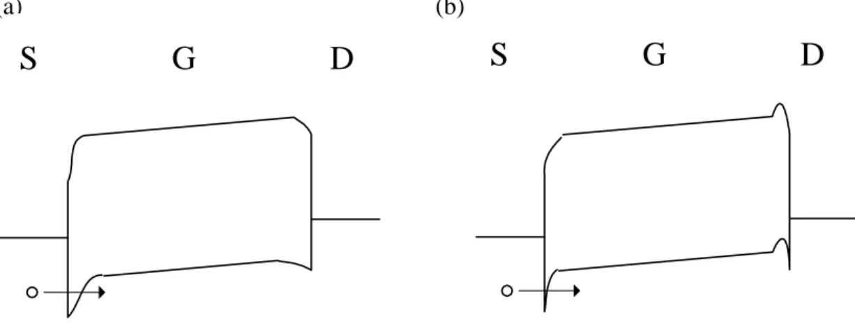
(11) Figure Captions Chapter 1 Fig. 1-1 (a)~(b) The Schematic band diagrams of SB and P-type MSB TFTs. (a) on-state of SB TFTs, (b) on-state of P-type MSB TFTs. Fig. 1-2 (a)~(b) The Schematic band diagrams of SB and P-type MSB TFTs. (a) off-state of SB TFTs, (b) off-state of P-type MSB TFTs,. Chapter 2 Fig. 2-1 MSB TFT process flow. Fig. 2-2 Id-Vg curve of (a) P-type, (b) N-type SB TFTs (SB TFTs) with Channel length=5um, Channel width=5um. Fig. 2-3 Schematic structure of device layout Fig. 2-4 Cross-section TEM of MSB TFTs Fig. 2-5 (a)~(b) The EDX analysis of MSB TFTs. Fig. 2-6 Electron diffraction pattern of Ni-silicided at (a) Gate region, (b) S/D region. Fig.2-7 SIMS depth profile of boron at gate region.. Chapter 3 Fig. 3-1 (a) The output characteristics of MSB pTFTs, (b) the output characteristics of MSB nTFTs. The implant dose=5×1015cm-2. The activation temperature is 600℃ and the activation time is 30 sec in RTA. Channel length=5um and Channel width=5um. Fig. 3-2 (a) Id-Vg curve of P-type CN TFTs, SB TFTs, and MSB pTFTs, (b) Id-Vg curve of N-type CN TFTs, SB TFTs, and MSB nTFTs. The implant dose=5× 1015cm-2. The activation temperature is 600℃ and the activation time is 30 sec in RTA. Channel length=5um and Channel width=5um. Fig. 3-3 (a)~(b) The transfer characteristics of (a) P-type, and (b) N-type MSB TFTs x.
(12) with different activation temperature. The implant dose=5×1015cm-2, activation time=30 sec in RTA. Channel length=5um and Channel width=5um. Fig. 3-4 (a)~(d) The Plane-View SEM micrographs of Source/Drain and Gate electrode of MSB nTFTs in the different activation temperature with implant Source: P+, the implant dose=5×1015cm-2, doping activation time: 30 sec in RTA. (a) 600℃ activation temperature. (b) 650℃ activation temperature (c) 700℃ activation temperature. (d) 750℃ activation temperature. Fig. 3-5 Schematic cross-view of agglomeration process over (a) buried oxide, (b) a-Si layer at high temperature Fig.3-6 (a)~(b) The transfer characteristics of (a) MSB pTFTs, and (b) MSB pTFTs with different doping activation time. The implant dose=5 × 1015cm-2, activation temperature=600℃ in RTA. Channel length=5um and Channel width=5um. Fig.3-7 (a)~(b) The transfer characteristics of (a) MSB pTFTs, and (b) MSB nTFTs with different doping concentration. The activation temperature=600℃, activation time=30 sec in RTA. Channel length=5um and Channel width=5um. Fig. 3-8 Threshold voltage roll off vs. channel width. The implant dose=5×1015cm-2. The channel length is 5um and Vtho is defined as threshold voltage of MSB pTFTs and MSB nTFTs with Channel length=5um and Channel width=10um. Fig. 3-9 Threshold voltage roll off vs. channel length. The implant dose=5×1015cm-2. The channel width is 5um and Vtho is defined as threshold voltage of MSB. xi.
(13) pTFTs and MSB nTFTs with Channel length=10um and Channel width=5um.. Chapter 4 Fig. 4-1 The film thickness with different deposition temperature and different implant dose. Fig. 4-2 The etch rate of HfO2 film of different deposition temperature and implantation condition. Fig. 4-3 Thickness change of HfO2 film after PDA process Fig. 4-4 (a)~(b) Thickness change of 400℃ film. The implant source is BF2+ in Fig. 4-4(a) and the implant source is Ar+ in Fig. 4-4(b) Fig . 4-5 (a)~(b) Thickness change of 500℃ film. The implant source is BF2+ in Fig. 4-5(a) and the implant source is Ar+ in Fig. 4-5(b) Fig . 4-6 (a)~(b) The wet etch rate of 400℃ film. The implant source is BF2+ in Fig. 4-6(a) and the implant source is Ar+ in Fig. 4-6(b) Fig . 4- 7 (a)~(b) The wet etch rate of 500℃ film. The implant source is BF2+ in Fig. 4-7(a) and the implant source is Ar+ in Fig. 4-7(b). xii.
(14) Chapter 1 Introduction 1.1 Overview Since the first demonstration in 1966 [1], polycrystalline silicon thin-film transistors (poly-Si TFTs) have attracted much attention. Over the past two decades, poly-Si TFTs have been widely used in various application fields, including thermal printer heads [2], linear image sensors [3], photo-detector amplifier [4], and scanners [5]. Poly-Si TFTs can also be applied in some memory ICs such as dynamic random access memories (DRAMs) [6], static random access memories (SRAMs) [7], electrical programming read only memories (EPROMs) [8], and electrical erasable programming read only memories (EEPROMs) [9]. Especially, the application in AMLCDs is the major reason to push poly-Si TFTs technology progressing rapidly [10]. Similar to amorphous silicon thin-film transistors (a-Si:H TFTs), the process of poly-Si TFTs is compatible with the conventional silicon technology. The higher mobility is the primary advantage of poly-Si TFTs compared with a-Si:H TFTs [11]. The mobility of a-Si:H TFTs is just about 1 cm2/V-s. However, the mobility of poly-Si TFTs higher than 10 cm2/v-s is easily achieved by present technologies [12-14]. The higher mobility is obtained by thin films deposited in the amorphous state and then crystallized into poly-Si type. In this case, the grain size is larger than that of thin films deposited in the polycrystalline state directly. However, in order to be realized on inexpensive glass substrate, the process temperature below 600℃ is urgent to be developed [15]. In the following, three kinds of low temperature crystallization methods are roughly reviewed. They are solid phase crystallization (SPC) [12], excimer laser crystallization (ELC) [13], and metal induced crystallization (MIC) [14].. 1.
(15) For the SPC process, the maximum process temperature is 600℃. Because the amorphous thin film is deposited at temperature below 600℃,thermal crystallization for 24 hr is required to transfer the amorphous thin film into the polycrystalline thin film [16]. The grain size is larger than that with the higher structural disorder of the amorphous thin film [17]. Compatible with the silicon technology and without extra cost are the advantages of the SPC process. Good uniformity and smooth surface are the other two advantages. However, the crystallization time is so long (>20 hr) so that the throughout is quite low and a lot of defects produced in this long time process [18]. Compared with the SPC process, the maximum process temperature of excimer laser crystallization (ELC) can be reduced below 600℃ [19]. Strictly speaking, the ELC process is not a low temperature process. With the excimer laser annealing, the silicon is heated well above 1200℃. However, due to the short time of laser pulse, the high temperature is maintained for a very short period. The thermal energy will not propagate to damage the glass substrate. During the ELC process, the silicon layer absorbs UV light strongly but the substrate composed of SiOx mostly reflects UV light. The amorphous thin film gains laser energy fast and transfers into poly-Si thin film quickly. The throughput ELC process is higher than that of the SPC process and the larger grain size translates to fewer defects. The laser energy density has a profound influence on the TFT devices [20]. The narrow laser process window is a major disadvantage of the ELC process. The high initial facility cost and high process complexity are the other two disadvantages of the ELC process [21]. The metal induced crystallization (MIC) process is another choice to transfer the amorphous thin film into poly-Si thin film with large grain size [22-23]. With the MIC process, metal, such as Ni, Al, and Cu is deposited on the amorphous thin film [14, 22-23]. The reaction between the metal and the amorphous thin film occurs by diffusion. With the interaction of the free election of the metal and the covalent Si. 2.
(16) bonds near the growing interface, the poly-Si grains grow. Considering the metal-Si eutectic temperature , the process temperature can be below 600℃ [24]. Compared with the other two processes, the process temperature of MIC process can be lower than that of SPC process and the process window of MIC process is larger than that of ELC process. However, the metal contamination is a profound influence on the application of the MIC process [25]. Besides this, the high defect density is another problem. With the scale down of device channel dimension, the device characteristic is improved. However, due to the existence of grain boundary, the dangling bonds trap free carriers and generate some potential barriers in the poly-Si thin film. These defects affect the performance such as on-state current, threshold voltage, and mobility seriously. In addition, junction leakage current due to carrier generation at source and drain increases the off-state current [26].. 1.2 Motivation Dozens of researches have been conducted to improve TFTs device performance. The grain size can be enlarged and the defects can be decreased by some crystallization techniques, such as excimer laser crystallization (ELC), solid phase crystallization (SPC), rapid thermal annealing (RTA), and metal induced crystallization (MIC). The plasma passivation in ammonia plasma can repair the dangling bonds and increase the reliability. Besides these two process technologies, another method can be used to improve the device performance.. 1.2.1. Modified-Schottky-Barrier Poly-Si TFT. MSB FinFET has been demonstrated to have excellent electrical characteristics [27]. With implant-to-silicide (ITS) process and suitable activation process, ultra shallow S/D extension (SDE) is formed to bridge the inverted channel and S/D region. 3.
(17) and modify the Schottky Barrier thickness. Therefore, the excellent I-V characteristics of MSB FinFET is obtained. In order to understand the theorem of Modified-Schottky -Barrier (MSB) further, Fig.1-1 and Fig.1-2 shows the band diagrams of SB and p-type MSB FinFET (MSB pFinFET) in the on-state and off-state modes. In Fig.1-1, the on-state current of SB FinFET is mainly due to the tunneling mechanism. In the pMSB FinFET, due to the high doping concentration of the SDE region, the barrier is thinner; therefore, carrier injection resistance from source to channel decreases, and then the on-state current is improved. In the off-state mode shown in Fig.1-2, for the SB FinFET, the leakage mechanism of SB FinFET is due to the thermionic emission from drain region at room temperature. In the high electric field, the field emission dominates the leakage mechanism. However, in the MSB pFinFET, the SDE region makes the Schottky barrier wider and higher so that the off-state current is lower than that of the conventional SB FinFET, and then off-state current is suppressed. With the high on-state current and lower off-state current, device with excellent electrical characteristics is achieved. Based on the similar structure of FinFET and TFT devices, it is natural to apply the MSB process to TFTs. The low thermal budget feature of MSB process is also compatible with the requirement of low temperature poly-Si TFTs (LTPS TFTs). We apply this technique to TFT device and expect to solve the disadvantages of conventional TFT (CN TFT) and Schottky Barrier TFT (SB TFT) discussed below. For CN TFT, the trap states near the Source/Drain region cause the junction leakage current [28]. The high resistance of the Source and Drain region reduces the device performance seriously. With the silicide process of the Source/Drain region, the resistance of Source/Drain drops off remarkable. However, for SB TFT, due to the am-bipolar characteristics of SB TFT, it’s quite hard to turn off when device is operated in the off-state mode. In the MSB TFT, the SDE region is so shallow and the doping concentration is so high that there are few trap states inside. With. 4.
(18) Modified-Scbottky-Barrier, the am-bipolar characteristics of SB TFT can be suppressed when the device is operated in the off-state mode. Therefore, MSB TFTs with excellent electrical characteristics is also expected.. 1.2.2. Wet etching of HfO2 experiments. For the gate dielectric process, the low temperature process results in lower breakdown voltage and higher leakage current compared with the high temperature process. In order to improve this issue, many researches have been conducted [29~30]. However, the breakdown voltage of the gate dielectric film deposited in the low temperature process can still not compared with that deposited in the high temperature process. That’s the reason why the thickness of the gate dielectric film in thin film transistors is still much thicker than that in conventional CMOS. After channel crystallization process, grain boundaries make the channel surface roughness. The rough surface causes high local electrical field and degrades breakdown voltage and mobility further [31]. Thicker gate dielectric film increases breakdown voltage but degrades device performance. Besides this, due to the existence of grain boundaries, the mobility of poly-Si TFTs is still lower than that of CMOS. Just like the crystallization methods mentioned above, ELC and MILC processes can enlarge the grain sizes and increase the mobility. However, the improvement of the mobility still has its limitation [32]. Upon these reasons, the dielectrics with higher permittivity such as HfO2, Ta2O5, etc. are considered to be used as gate dielectric [33]. Under the same or even smaller effective oxide thickness (EOT), the physical thickness of the high-k gate dielectric can be much thicker so that the gate leakage current is suppressed and the gate breakdown voltage is elevated. Besides this, the on-state current could be higher than that of the conventional poly-Si TFTs with SiO2 gate dielectric. Although the mobility degradation is a serious problem for high-k dielectric to be. 5.
(19) applied in the CMOS technology, this problem may be ignored in TFTs. The mobility degradation with high-k gate dielectric is due to the interfacial layer and remote phonon scattering [34]. In the conventional poly-Si TFTs, the main mechanism of low mobility is scattering due to grain boundaries and rough channel surface. Applying high-k dielectric in poly-Si TFTs, the effect of remote phonon scattering will be not significant. Because the effective oxide thickness in poly-Si TFTs is not necessary to be as thin as that in CMOS, interfacial layer formation between high-k dielectric and poly-Si channel can be avoided by inserting a thin SiO2 buffer layer. In this case, remote phonon scattering can be further reduced. Since the high-k gate dielectric process is a low temperature process, this process can be immediately applied to LTPS TFTs. Lots of high-k dielectrics have been proposed [35]. Among all high-k dielectric candidates, HfO2 is the most promising candidate with many advantages such as suitable permittivity, acceptable band alignment, high free energy of reaction with Si, high heat of formation, and superior thermal stability with poly-Si [36]. However, unlike SiO2, how to remove HfO2 layer after gate patterning is a serious problem that should be solved as soon as possible. In 2003, Andrew J. Kellock et al proposed that HfO2 can be etched by Ar+ bombardment and diluted-HF solution [37]. Ar+ bombardment is used to damage the crystallized HfO2 film. Then, the damaged HfO2 film is etched by diluted-HF solution. However, the etching rate selectivity between HfO2 and SiO2 using diluted HF solution is very poor. Furthermore, Ar+ bombardment is not standard process for Si technology. In this thesis, some detailed experiments are performed. Without using diluted HF solution, HF/IPA solution is much more useful to etch HfO2 film due to its higher etch selectivity [38]. Ar+ and BF2+ ions from ion implanter were used to damage the HfO2 film. BF2+ ion sources are believed to have much more advantages than Ar+ in the CMOS technology. Unlike Ar+ as a carrier gas, BF2+ can not only damage HfO2. 6.
(20) film but also can be use to dope source/drain (S/D) region.. 1.3 Thesis organization In chapter 2, the fabrication of MSB TFT is presented and the structural analysis is examined. In chapter 3, the performance of Modified-Schottky-Barrier (MSB) Poly-Si TFT, Schottky barrier TFT, and conventional TFT are compared. Some more detail electrical characteristics of MSB TFT are discussed. The effects of process conditions on the performance of MSB TFT are also discussed. The etching mechanism of HfO2 film is shown in chapter 4. Finally, chapter 5 gives the conclusions of this thesis and suggests some future works.. 7.
(21) (a). S. (b). G. S. D. G. D. Fig. 1-1 (a)~(b) The Schematic band diagrams of SB and P-type MSB TFTs. (a) on-state of SB TFTs, (b) on-state of P-type MSB TFTs. (a). S. (b). G. S. D. G. D. Fig. 1-2 (a)~(b) The Schematic band diagrams of SB and P-type MSB TFTs. (a) off-state of SB TFTs, (b) off-state of P-type MSB TFTs,. 8.
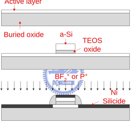
(22) Chapter 2 Fabrication of Modified Schottky Barrier Polycrystalline Silicon Thin-film Transistors (MSB TFTs) 2-1 Introduction Modified-Schottky-Barrier FinFET (MSB FinFET) has been demonstrated to have the excellent electrical characteristics [27]. Ultra shallow source/drain (S/D) extension (SDE) of MSB FinFET bridges the inverted channel and S/D region and modifies the Schottky barrier thickness. Therefore, excellent electrical characteristic is obtained. Besides these, ultra shallow SDE can be formed at temperature as low as 600℃, the low thermal budget allows this technique to apply in TFT device. In this chapter, the fabrication of Modified-Schottky-Barrier Poly-Si TFTs is presented. The structure analysis is also discussed in this chapter.. 2-2 Experimental Procedure 2-2-1 Fabrication of MSB TFTs Fig.2-1 shows the schematic process flow of the MSB TFT. In order to simulate the glass substrate, a 1um thick oxide was deposited on 6-in wafer first. Then, a 50 nm thick a-Si layer was deposited as device active layer in a low pressure chemical vapor deposition (LPCVD) system at 550℃ using SiH4 as Si source. The active layer was crystallized by solid phase crystallization (SPC) process at 600℃ for 24 hours in N2 ambient. After patterning the active layer, a 50 nm thick TEOS oxide layer was deposited in a LPCVD system at 700℃ as gate oxide. A 100 nm thick a-Si layer was 9.
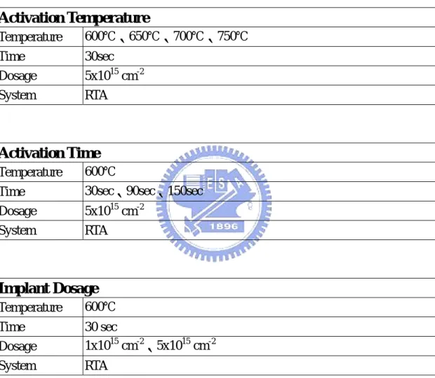
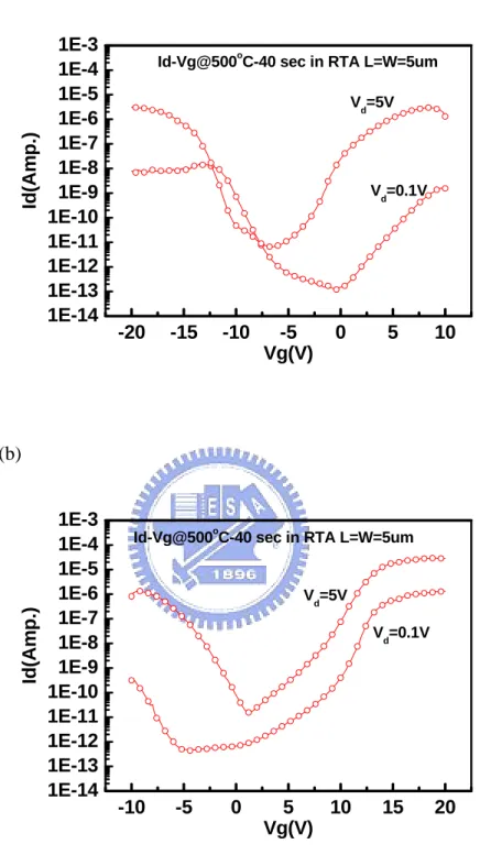
(23) subsequently deposited in another LPCVD system at 550℃ using SiH4 as Si source as gate electrode. Then, the a-Si gate electrode layer and the gate oxide layer were etched in a poly-Si etcher of model TCP-9400 and an oxide etcher of model TEL-5000, respectively. To form a sidewall spacer to avoid the bridging effect between gate and S/D in the following NiSi silicidation process, a 100 nm thick TEOS oxide was deposited in a LPCVD system at 700℃ followed by dry etching process. A 22nm-thick Ni film was then deposited in a sputtering system immediately after a diluted-HF dip for 40 sec. The spacer length was reduced to about 50-60 nm after the diluted-HF dip process. The Si layer at S/D region was converted to NiSi completely by a rapid-thermal annealing at 500℃ for 40 seconds in N2 ambient. After the silicidation process, the un-reacted Ni was selectively removed by H2SO4/H2O2 solution for 10 minutes at 100~120 ℃ . Fig.2-2 shows the Id-Vg characteristic of a device with 5 um channel length and 5um channel width measured at this stage. The am-bipolar characteristic indicates that a typical Schottky barrier (SB) device has been fabricated successfully. Implant-to-silicide (ITS) process was employed to form MSB junction. BF2+ ions were implanted at 45 KeV for p-channel MSB TFTs (MSB pTFTs) and P+ ions were implanted at 30KeV for n-channel MSB TFTs (MSB nTFTs). Two dosages of 1x10¹⁵ and 5x1015 cm-2 were used to study the effect of implantation dose. Dopants were then diffused out of silicide to form an ultra-shallow SDE at the channel-S/D interface by a low temperature annealing process in N2 ambient. This process was performed in a RTA system at temperatures of 600, 650, 700 and 750℃ for 30, 90, and 150 sec. Table 2-1 summarizes the process conditions studied in this thesis. In order to simply the fabrication process, source, drain, and gate electrodes were defined large enough so that devices can be measured directly without additional metallization process. The typical layout of devices is shown in Fig.2-3.. 10.
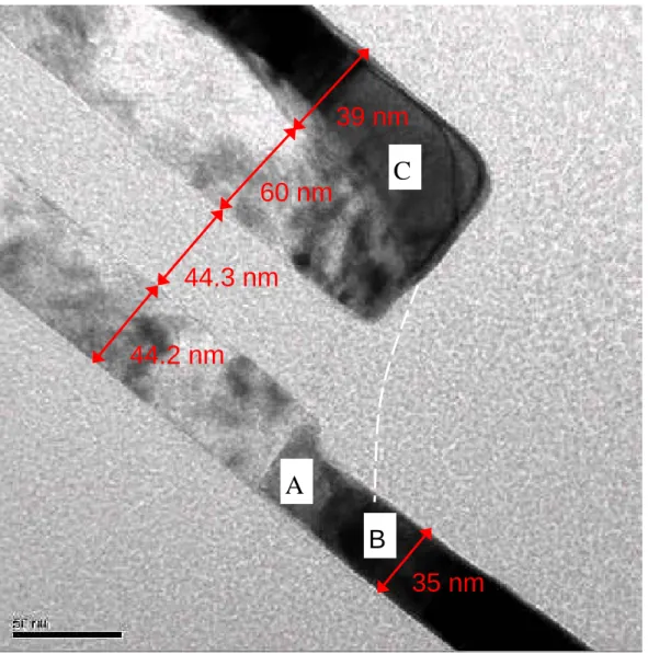
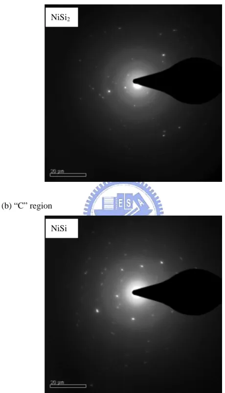
(24) 2-2-2 Fabrication of Conventional TFTs Besides the fabrication of MSB TFTs and SB TFTs, conventional (CN) TFTs were also fabricated for comparison purpose. The process steps for CN TFTs were identical to those for MSB and SB TFTs until spacer formation. S/D and gate were doped by BF2+ ion implantation at 25KeV to a dose of 5x1015 cm-2 for pTFTs and P+ ion implantation at 18 KeV to a dose of 5x1015 cm-2 for nTFTs. In order to activate dopants, a 300 nm thick TEOS oxide was deposited in a plasma enhanced chemical vapor deposition (PECVD) system at 300℃ followed by a furnace annealing for 12 hours at 600℃ in N2 ambient for CN pTFTs and by a RTA annealing for 20 seconds at 700 ℃ in N2 ambient for CN nTFTs. Finally, typical contact opening and metallization processes were performed to complete the device fabrication. A 30 minutes alloy process was carried out at 400℃ for reducing the contact resistance.. 2-2-3 Structural Analysis of MSB TFTs Fig.2-4 shows the cross-sectional transmission electron microscopy (TEM) micrographs of a MSB nTFT with gate length (Lg) of 5um, gate width (Wg) of 5um, and channel thickness (Tch) of 50nm. The oxide sidewall spacer is indicated by white dashed line. It is clear that the S/D region was fully silicided and a 50 nm thick NiSi was formed on a-Si gate. The slight sunken of S/D near gate edge is due to the micro-trenching effect during the plasma etch of gate oxide. Fig.2-5(a) and (b) show the energy dispersive X-ray (EDX) spectra of region A and region B as indicated in Fig.2-4, respectively. Region B is Ni-silicide and region A is still poly-Si. It is confirmed by the EDX spectra that the lateral growth of Ni-silicide is limited and the S/D silicide does not overlap with gate electrode. The phase of silicide at S/D region and gate region were identified to be NiSi2 and NiSi, respectively, by electron diffraction pattern as shown in Fig.2-6. This result is identical with that observed in MSB FinFET [27] and the mechanism is still under investigation.. 11.
(25) The silicide layer on a-Si gate is about 45 nm, leaving unreacted a-Si of about 74 nm thick. Fig.2-7 shows the secondary ion mass spectroscopy (SIMS) depth profile of boron at gate region. The implantation dose is 5x1015 cm-2 and the activation condition is RTA at 600℃ for 30 sec in N2 ambient. It is observed that most of the boron atoms were confined in Ni-silicide and only a very shallow p-type layer formed at the Ni-silicide/a-Si interface. It is expected that the ultra-shallow SDE at S/D region should be similar. It should be noted that since the a-Si gate was not doped before silicidation, gate depletion becomes unavoidable and device performance will be suffered. All of the device performance of MSB TFTs presented in the next chapter could be improved if the a-Si gate electrode were heavily doped in advance.. 12.
(26) Table 2-1 Experimental split condition of MSB TFTs. Activation Temperature Temperature. 600℃、650℃、700℃、750℃. Time. 30sec. Dosage. 5x1015 cm-2. System. RTA. Activation Time Temperature. 600℃. Time. 30sec、90sec、150sec. Dosage. 5x1015 cm-2. System. RTA. Implant Dosage Temperature. 600℃. Time Dosage. 30 sec 1x1015 cm-2、5x1015 cm-2. System. RTA. 13.
(27) Active layer. Buried oxide. a-Si. TEOS oxide. BF2+ or P+ Ni Silicide. SDE. Fig. 2-1 MSB TFT process flow.. 14.
(28) Id(Amp.). (a) 1E-3 1E-4 1E-5 1E-6 1E-7 1E-8 1E-9 1E-10 1E-11 1E-12 1E-13 1E-14. o. Id-Vg@500 C-40 sec in RTA L=W=5um Vd=5V. Vd=0.1V. -20. -15. -10. -5 Vg(V). 0. 5. 10. Id(Amp.). (b) 1E-3 1E-4 1E-5 1E-6 1E-7 1E-8 1E-9 1E-10 1E-11 1E-12 1E-13 1E-14. o. Id-Vg@500 C-40 sec in RTA L=W=5um. Vd=5V Vd=0.1V. -10. -5. 0. 5 10 Vg(V). 15. 20. Fig. 2-2 Id-Vg curve of (a) P-type, (b) N-type SB TFTs (SB TFTs) with Channel length=5um, Channel width=5um.. 15.
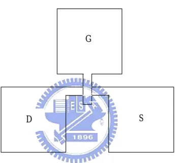
(29) G. S. D. Fig. 2-3 Schematic structure of device layout. 16.
(30) 39 nm C. 60 nm 44.3 nm 44.2 nm. A B 35 nm. Fig. 2-4 Cross-section TEM of MSB TFTs. 17.
(31) (a). (b). Fig. 2-5 (a)~(b) The EDX analysis of MSB TFTs.. 18.
(32) (a) “B” region NiSi2. (b) “C” region NiSi. Fig. 2-6 Electron diffraction pattern of Ni-silicide at (a) S/D region, ”B” (b) Gate region “C”.. 19.
(33) (Angstrom). Fig.2-7 SIMS depth profile of boron at gate region.. 20.
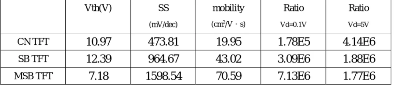
(34) Chapter3 Electrical Characteristics of MSB TFT In this chapter, the electrical characteristics of CN TFTs, SB TFTs, and MSB TFTs are compared at first. Then, the effect of MSB process conditions including activation temperature, activation time, and implantation dose are presented and discussed. Device parameters including threshold voltage (Vth), subthreshold swing (S.S.), mobility, and on/off current ratio are all extracted. The Vth is defined as the gate voltage at which Ids/W=10 nA and 100 nA as Vds=0.1V and 5V, respectively. The S.S. is defined as the minimum value of the inverse of derivative of ∂log10(Ids)/∂Vgs. Mobility is extracted from the maximum transconductance at Vds=0.1V. The on/off current ratio is defined as the ratio of the maximum value of Ids and the minimum value of Ids. On/off current ratios at Vds=0.1V and 5V were both extracted.. 3-1 Basic Electrical Characteristics Fig.3-1(a) and (b) shows the output characteristics of MSB pTFT and MSB nTFT, respectively, with channel length (Lg) of 5um and channel width (Wg) of 5um. With SDE region bridging the inverted channel and S/D region and reducing the Schottky barrier thickness, the carrier injection resistance from source to channel is reduced greatly so that the typical sub-linear phenomenon of SB TFTs is not observed upon MSB TFTs. Fig.3-2 compares the transfer characteristics of CN, SB, and MSB TFTs. The extracted parameters are listed in Table 3-1 and Table 3-2. In the p-channel devices, MSB TFTs shows the best performance among MSB, SB and CN TFTs no matter in the subthreshold swing (S.S.), field-effect mobility, or on/off current ratio. The low driving current and high leakage current of SB TFT is as expected. Because the 21.
(35) driving current is too poor, mobility of SB TFT can not be extracted. The low mobility of CN TFT is attributed to the high S/D resistance while the poor S.S. of CN TFT may be due to different grain structure in channel region because of different thermal budget. The high S/D resistance of CN TFT can also explain the low driving current in comparison with MSB TFT. The leakage current of MSB TFT is almost identical with that of CN TFT and is much lower than that of SB TFT. It is pronounced that the MSB structure can produce excellent TFTs. In the n-channel TFTs, MSB TFT also exhibits the highest driving current and the lowest leakage current among the three kinds of devices. It should be noted that the on/off current ratios of MSB pTFT exceeds 107 and MSB nTFT exceeds 7×10⁶, both are compatible with those reported results as the channel is crystallized by SPC process. In this thesis, the SB and MSB TFTs did not experience hydrogen-contained plasma treatment after device fabrication. The trap states are not passivated by hydrogen. At high drain voltage, electron-hole pairs are generated so that the potential of floating body increases and then the DIBL-like effect occurs. As mentioned in chapter 2 that the un-silicided Si layer of gate electrode is almost undoped. Gate depletion becomes unavoidable. It is thus expected that the performance of MSB devices could be improved further is the Si channel is crystallized by ELA or MILC method and the Si gate is heavily doped before silicide formation. Fully-silicided (FUSI) gate is another possible strategy [39].. 3-2 Effects of MSB Process Parameters 3-2-1 Activation Temperature Temperature is the most important process parameters to form ultra shallow SDE and to activate dopant. Since there are few researches about behaviors of. 22.
(36) phosphorus and boron in Ni-silicide, a heavy dose of 5x1015cm-2 is used to study the effect of activation temperature in order to avoid the influence of insufficient dopants. The transfer characteristics of MSB pTFTs and nTFTs experienced different activation temperatures are shown in Fig.3-3(a) and (b), respectively. The extracted parameters of MSB pTFTs and MSB nTFTs are presented in Table 3-3 and Table 3-4, respectively. It is observed that RTA at 600℃ and 650℃ result in the best device performance for both pTFTs and nTFTs. The slight deviation of Vth, S.S., mobility, as well as on/off current ratio may come from the process deviation. By increasing the RTA temperature to higher than 700℃, device performance degrades dramatically. Increase of absolute value of Vth, increase of S.S., and decrease of mobility are clearly observed. However, the off-state current (Ioff) slightly decreases with the increase of RTA temperature. It is known that the Ioff of MSB devices is determined by the quality of the MSB junction. The continuous reduction of Ioff implies that the higher activation temperature results in deeper and higher concentration SDE. Since the S/D integrity is maintained, the device degradation mechanism must be related to the gate electrode. The first speculation about the degradation mechanism of S.S. and mobility is the degradation of surface state quality of channel. It was reported that thermal stress of gate electrode may generate oxide charge and interface state defects [40~41]. However, no matter positive charges or negative charges were generated by thermal stress, the Vth of MSB pTFTs and MSB nTFTs should shift toward the same direction. According to the measured results, the absolute value of Vth increases with the increase of activation temperature. That is the Vth of MSB pTFTs and MSB nTFTs shift toward opposite direction. Therefore, the thermal stress induced degradation is ruled out. It is known that the thermal stability of Ni-silicide is not as good as Ti-silicide or. 23.
(37) Co-silicide [42]. Annealing at temperatures higher than 700℃ usually results in agglomeration of Ni-silicide [43~44]. It is postulated that he agglomeration of silicide at gate electrode may degrade device performance. Fig.3-4 shows the surface morphology of MSB TFTs inspected by scanning electron microscope (SEM) after annealing at different temperatures. The agglomeration of silicide at gate region occurs when the activation temperature is above 700℃; while the silicide at S/D region keeps continuous at 750℃. The un-agglomeration of silicide at S/D region is consistent with the non-degradation of Ioff. Since the Si gate was not doped before silicide formation, once the silicide at gate region agglomerated, gate voltage can not be applied to the gate region without silicide. Therefore, higher gate voltage is required to form inverted channel at he active layer above where the silicide film is broken. That’s why the absolute value of Vth increases for both pTFTs and nTFTs with the increase of activation temperature. The degradation of S.S. and mobility can also explained by the same mechanism. There are two possible reasons can explain the different thermal stability at gate region and S/D region. The first one is thermal stress [45~46]. The vertical structures at gate region and S/D region are different. At gate region, Ni-silicide is stacked on un-reacted a-Si layer, TEOS gate oxide, Si active layer, and buried oxide, while the Ni-silicide at S/D region is stacked on buried oxide only. The thermal stress is quite different at high temperature. It is also reported that the NiSi film is easier to be agglomerated than the NiSi2 [47~48]. Anyway, it is quite possible that the thermal stress at gate region is higher than that at S/D region, therefore, thermal stress induced agglomeration may occur at gate region earlier. Another possible reason is more complex. We use the schematic cross-sectional structure of Fig.3-5 to explain it [49]. The agglomeration of silicide on Si substrate proceeds with three steps : (a) metal-Si bonds break due to thermal energy, (b) metal diffuse along grain boundary and silicide/Si interface, (c) new metal-Si bonds form at. 24.
(38) suitable position until energy balance between grain boundary and interface energy. At gate region, there are un-reacted Si layer under Ni-silicide. Similar procedure can occur as shown in Fig.3-5(a). Upon high temperature process, Ni-Si bonds break and Ni atoms diffuse along grain boundaries until the energy balance between the grain boundary energy and both surface and a-Si layer interface energies is achieved. Therefore, groove morphology proceeds and enlarges NiSi grain until NiSi island forms. However, at S/D region, there is no silicide/Si interface and no excess Si atoms to react with un-bonded Ni atoms as shown in Fig.3-5(b). Therefore, agglomeration is suppressed. Certainly, it is possible that both reasons exist in our case. To identify which one is the root cause needs more works. We can have a short summary now. A 600℃ or 650℃ RTA is sufficient to form excellent MSB pTFTs and nTFTs simultaneously. The fully silicided S/D region can sustain thermal annealing up to 750℃. If gate electrode is also fully silicided, the sustainable process temperature is expected to be 750℃ at least. For the application of LTPS TFTs, 600℃ is chosen to be the process temperature of MSB process.. 3-2-2 Activation Time Fig.3-6 (a) and (b) show the transfer characteristics of p-channel and n-channel MSB TFTs with different activation times, respectively. Extracted parameters are listed in Table 3-5 and Table 3-6. For MSB pTFTs, a 30 sec activation is sufficient to achieve superior performance and the on/off current ratio can be higher than 107. However, it seems that device performance degrades with the increase of activation time. One of the possible causes is dopant deactivation [50]. In poly-Si, grain boundaries act as sinks for impurity atom segregation and also trap carriers at defects caused by incomplete atomic bonding. The thermal equilibrium concentration for dopants increases with temperature and the major driving force for deactivation is dopant supersaturation. In the ITS process, dopants were implanted into silicide and. 25.
(39) then diffused out of silicide and piled-up at the silicide/Si interface. It is possible that some of the piled-up dopants distribute in the poly-Si grains and some of the piled-up dopants fill grain boundaries in the short activation period. With the longer activation time, more dopants were trapped by defects or grain boundaries. These trapped dopants are electrically deactive so that the device performance degrades. For n-channel MSB TFTs, similar to p-channel MSB TFTs, ultra shallow SDE forms after a short activation time of 30 seconds. Unlike boron, phosphorus has slower diffusion rate. A 30 sec activation may be not sufficient to form intact SDE. By increasing activation time, dopant diffuse out of silicide and all of the Ni-silicide grains are surrounded by SDE. Therefore, some device characteristics such as S.S. and Ioff are improved. For the reduction of mobility and on-state current (Ion), dopant deactivation is still a possible reason. Although Ion slightly reduces, the on/off current ratio increases with the increase of activation time. This is due to the obvious reduction of Ioff. According to the above discussion, 30 seconds RTA is a suitable activation time for MSB TFTs.. 3-2-3 ITS Dosage In order to form effective SDE, high dose implantation is necessary. Similarly, high concentration SDE is also necessary to modify Schottky Barrier. In this thesis, ITS dosages of 1x1015cm-2 and 5x1015cm-2 are considered. The activation temperature is 600℃ and the activation time is 30 sec. The transfer characteristics of MSB pTFTs and MSB nTFTs are shown in Fig.3-7(a) and (b), respectively. The corresponded parameters are listed in Table 3-7 and Table 3-8. In general, device characteristics of devices with different dosages are very similar. The major difference is the Ioff at low Vds. Lower implantation dose results in slightly higher Ioff due to lower SDE concentration. However, at high Vds, energy band bending of the MSB formed with. 26.
(40) different implantation doses are similar, there is no difference in device performance between these two implantation doses. The low implantation dose also results in lower mobility of n-channel MSB TFTs due to the slow diffusion rate of phosphorus and thus the low concentration SDE with a 30 seconds RTA.. 3-2-4 Geometric Effect In this subsection, the effects of Wg and Lg on threshold voltage are discussed. Fig.3-8 shows threshold voltage as a function of Wg. Slight Vth decrease is observed as Wg decreases. It is known that the potential barrier in the channel determines Vth of poly-Si TFTs [51]. Therefore, the narrower Wg has fewer grain boundaries and trap states so that Vth decreases slightly. On the contrary, Vth increases as channel length decreases as shown in Fig.3-9. Unlike short channel effect of conventional MOSFETs, strong reverse short channel effect appears. This phenomenon may be explained by the metal-induced crystallization (MIC)/metal-induced lateral crystallization (MILC) interfacial grain boundaries (MMGB’s) effect [52]. In the silicidation process of MSB TFTs, MIC, instead of MILC, which proceeds under spacer, occurs in the S/D region. The continuous MMGB’s are formed and are self-aligned to the edges of gate electrode. After ITS process and the following activation process, because of the overlap of MMGB’s and the channel, charge carriers fills MMGB’s trap states. Therefore, MMGB energy barrier is higher than barriers in the channel and the higher Vgs is required to inverse the channel. When Lg is reduced, a larger fraction of the channel comes under the influence of MMGB’s energy barrier. The Reverse short channel effect appears. Since reverse short channel effect is due to trap of carriers from ITS process exists in the MMGB’s, plasma treatment may passivate trap states and relax this effect.. 27.
(41) 3-3 Summary In this chapter, device performance of MSB TFTs has been represented. Some advanced electrical characteristics of MSB TFTs are also discussed. After ITS process, MSB TFTs with the suitable activation process shows the superior I-V characteristics compared to CN TFTs and SB TFTs. An activation temperature between 600℃ to 650℃ at RTA results in the best device performance for both MSB pTFTs and MSB nTFTs. While MSB TFTs are activated at the temperature higher than 700℃, Ni-silicide agglomerates at gate electrode and device performance degrades. Thermal stress and surface energy unbalance are the two possible mechanisms. At suitable activation temperature, 30 seconds RTA is a suitable activation time for MSB TFTs, It is possible that dopant deactivation occurs at longer activation time and decreases device performance. Besides these, higher implantation dose can provide more dopants to enhance device performance. Considering the device geometries, narrower channel width has few grain boundaries and trap states; therefore, threshold voltage slightly decreases. On the other hand, strong reverse short channel effect appears due to traps states of MMGB’s. In summary, MSB process can achieve excellent device performance and be applied to LTPS TFTs due to its low thermal budget feature.. 28.
(42) Table 3-1 The important parameters of CN, SB, and MSB pTFTs. Channel length=5um and Channel width=5um. MSB pTFTs of implant dose=5× 1015cm-2 was activated with the temperature of 600℃, 30 sec in RTA. The signal “X” shows the unreasonable value gotten from the I-V characteristic.. Vth(V). SS. mobility 2. Ratio. Ratio. (mV/dec). (cm /V•s). Vd=0.1V. Vd=5V. CN TFT. -14.94. 2031.45. 7.73. 2.71E6. 1.57E6. SB TFT. -14.04. 1127.9. X. 1.35E5. 4.85E5. MSB TFT. -6.74. 950.86. 33.62. 2.89E7. 1.52E7. Table 3-2 The important parameters of CN, SB, and MSB nTFTs. Channel length=5um and Channel width=5um. MSB nTFTs of implant dose=5× 1015cm-2 was activated with the temperature of 600℃, 30 sec in RTA.. Vth(V). SS. mobility 2. Ratio. Ratio. (mV/dec). (cm /V•s). Vd=0.1V. Vd=5V. CN TFT. 10.97. 473.81. 19.95. 1.78E5. 4.14E6. SB TFT. 12.39. 964.67. 43.02. 3.09E6. 1.88E6. MSB TFT. 7.18. 1598.54. 70.59. 7.13E6. 1.77E6. 29.
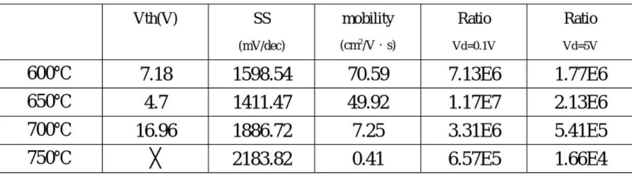
(43) Table 3-3 The parameters of MSB pTFTs in the different doping activation temperature. The implant dose=5×1015cm-2, activation time=30 sec in RTA. Channel length=5um and Channel width= 5um. Vth(V). SS. mobility 2. Ratio. Ratio. (mV/dec). (cm /V•s). Vd=0.1V. Vd=5V. 600℃. -6.74. 950.86. 33.62. 2.89E7. 1.52E7. 650℃. -8.51. 1028.08. 34.94. 1.93E8. 6.83E6. 700℃. -15.26. 1960.79. 9.71. 1.96E6. 8.61E5. 750℃. -19.54. 2783.31. 2.87. 3.97E5. 1.13E5. Table 3-4 The parameters of MSB nTFTs in the different doping activation temperature. The implant dose=5×1015cm-2, activation time=30 sec in RTA. Channel length=5um and Channel width= 5um. The sign “╳” represents the value out of the measurement range. Vth(V). SS. mobility. Ratio. Ratio. (mV/dec). (cm2/V•s). Vd=0.1V. Vd=5V. 600℃. 7.18. 1598.54. 70.59. 7.13E6. 1.77E6. 650℃. 4.7. 1411.47. 49.92. 1.17E7. 2.13E6. 700℃. 16.96 ╳. 1886.72. 7.25. 3.31E6. 5.41E5. 2183.82. 0.41. 6.57E5. 1.66E4. 750℃. 30.
(44) Table 3-5 The parameters of MSB pTFTs in the different doping activation time. The implant dose=5×1015cm-2, activation temperature=600℃ in RTA. Channel length=5um and Channel width=5um. Vth(V). SS. mobility 2. Ratio. Ratio. (mV/dec). (cm /V•s). Vd=0.1V. Vd=5V. 30 sec. -6.74. 950.86. 33.62. 2.89E7. 1.52E7. 90 sec. -7.07. 1038.62. 40.1. 6.32E7. 1.17E7. 150 sec. -10.61. 1268.7. 20.7. 4.01E6. 5.24E6. Table 3-6 The parameters of MSB nTFTs in the different doping activation time. The implant dose=5×1015cm-2, activation temperature=600℃ in RTA. Channel length=5um and Channel width=5um. Vth(V). SS. mobility. Ratio. Ratio. (mV/dec). (cm2/V•s). Vd=0.1V. Vd=5V. 30 sec. 7.18. 1598.54. 70.59. 7.13E6. 1.77E6. 90 sec. 6.23. 1539.79. 57.56. 6.87E6. 3.02E6. 150 sec. 8.33. 1188.82. 33.88. 3.26E7. 1.04E7. 31.
(45) Table 3-7 The parameters of MSB pTFTs with different doping concentration. The activation temperature=600℃, activation time=30 sec in RTA. Channel length=5um and Channel width=5um. Vth(V). SS. mobility 2. Ratio. Ratio. (mV/dec). (cm /V•s). Vd=0.1V. Vd=5V. 1×1015 cm-2. -6.51. 901.43. 34.11. 4.89E7. 1.34E7. 15. -6.74. 950.86. 33.62. 2.89E7. 1.52E7. -2. 5×10 cm. Table 3-8 The parameters of MSB nTFTs with different doping concentration. The activation temperature=600℃, activation time=30 sec in RTA. Channel length=5um and Channel width=5um. Vth(V). SS. mobility. Ratio. Ratio. (mV/dec). (cm2/V•s). Vd=0.1V. Vd=5V. 15. -2. 6.48. 1587.3. 45.53. 3.24E6. 1.52E6. 15. -2. 7.18. 1598.54. 70.59. 7.13E6. 1.77E6. 1×10 cm 5×10 cm. 32.
(46) Id(uA). (a) 60 55 50 45 40 35 30 25 20 15 10 5 0. Id-Vd@L=W=5um Vg=-20V. Vg=-16V. Vg=-12V. -20. -15. -10. -5. 0. Vd(V). Id(uA). (b) 150 140 130 120 110 100 90 80 70 60 50 40 30 20 10 0. Id-Vd@L=W=5um. Vg=20V. Vg=16V. Vg=12V. 0. 5. 10. 15. 20. Vd(V). Fig. 3-1 (a) The output characteristics of MSB pTFTs, (b) the output characteristics of MSB nTFTs. The implant dose=5×1015cm-2. The activation temperature is 600℃ and the activation time is 30 sec in RTA. Channel length=5um and Channel width=5um.. 33.
(47) Id(Amp.). (a) 1E-3 1E-4 1E-5 1E-6 1E-7 1E-8 1E-9 1E-10 1E-11 1E-12 1E-13 1E-14. Id-Vg@L=W=5um. CN TFT SB TFT MSB pTFT. -20. -15. -10. -5 Vg(V). 0. 5. 10. Id(Amp.). (b) 1E-3 1E-4 1E-5 1E-6 1E-7 1E-8 1E-9 1E-10 1E-11 1E-12 1E-13 1E-14. Id-Vg@L=W=5um. CN TFT SB TFT MSB nTFT. -10. -5. 0. 5 10 Vg(V). 15. 20. Fig. 3-2 (a) Id-Vg curve of P-type CN TFTs, SB TFTs, and MSB pTFTs, (b) Id-Vg curve of N-type CN TFTs, SB TFTs, and MSB nTFTs. The implant dose=5× 1015cm-2. The activation temperature is 600℃ and the activation time is 30 sec in RTA. Channel length=5um and Channel width=5um.. 34.
(48) Id(Amp.). (a) 1E-3 1E-4 1E-5 1E-6 1E-7 1E-8 1E-9 1E-10 1E-11 1E-12 1E-13 1E-14. +. 15. -2. Id-Vg@BF2 -5x10 cm ,RTA-30 sec L=W=5um. o. 600 C o 650 C o 700 C o 750 C. -20. -15. -10. -5 Vg(V). 0. +. 15. -2. -5. 0. 5 10 Vg(V). 5. 10. 15. 20. Id(Amp.). (b) 1E-3 1E-4 1E-5 1E-6 1E-7 1E-8 1E-9 1E-10 1E-11 1E-12 1E-13 1E-14. Id-Vg@P -5x10 cm ,RTA-30 sec L=W=5um o 600 C o 650 C o 700 C o 750 C. -10. Fig. 3-3 (a)~(b) The transfer characteristics of (a) P-type, and (b) N-type MSB TFTs with different activation temperature. The implant dose=5×1015cm-2, activation time=30 sec in RTA. Channel length=5um and Channel width=5um.. 35.
(49) (a). (b). (c). (d). Fig. 3-4 (a)~(d) The Plane-View SEM micrographs of Source/Drain and Gate electrode of MSB nTFTs in the different activation temperature with implant Source: P+, the implant dose=5×1015cm-2, doping activation time: 30 sec in RTA. (a) 600℃ activation temperature. (b) 650℃ activation temperature (c) 700℃ activation temperature. (d) 750℃ activation temperature.. 36.
(50) (a). (b) NiSi. NiSi. NiSi. NiSi. NiSi. NiSi2. NiSi2. NiSi2. a-Si. Oxide. a-Si. Oxide. a-Si. Oxide. a-Si. Oxide. NiSi2. NiSi2. NiSi. NiSi. Fig. 3-5 Schematic cross-view of agglomeration process over (a) a-Si layer, (b) buried oxide at high temperature. 37.
(51) Id(Amp.). (a) 1E-3 1E-4 1E-5 1E-6 1E-7 1E-8 1E-9 1E-10 1E-11 1E-12 1E-13 1E-14. +. 15. -2. o. Id-Vg@BF2 -5x10 cm ,RTA-600 C L=W=5um. 30 sec 90 sec 150 sec. -20. -15. -10. -5 Vg(V). 0. 5. 10. Id(Amp.). (b) 1E-3 1E-4 1E-5 1E-6 1E-7 1E-8 1E-9 1E-10 1E-11 1E-12 1E-13 1E-14. +. 15. -2. o. Id-Vg@P -5x10 cm ,RTA-600 C L=W=5um. 30 sec 90 sec 150 sec. -10. -5. 0. 5 10 Vg(V). 15. 20. Fig.3-6 (a)~(b) The transfer characteristics of (a) MSB pTFTs, and (b) MSB pTFTs with different doping activation time. The implant dose=5 × 1015cm-2, activation temperature=600℃ in RTA. Channel length=5um and Channel width=5um.. 38.
(52) Id(Amp.). (a) 1E-3 1E-4 1E-5 1E-6 1E-7 1E-8 1E-9 1E-10 1E-11 1E-12 1E-13 1E-14. +. o. Id-Vg@BF2 ,RTA-600 C-30 sec L=W=5um. 15. -2. 1x10 cm 15 -2 5x10 cm. -20. -15. -10. -5 Vg(V). 0. 5. 10. Id(Amp.). (b) 1E-3 1E-4 1E-5 1E-6 1E-7 1E-8 1E-9 1E-10 1E-11 1E-12 1E-13 1E-14. +. o. Id-Vg@P ,RTA-600 C-30 sec L=W=5um. 15. -2. 1x10 cm 15 -2 5x10 cm. -10. -5. 0. 5 10 Vg(V). 15. 20. Fig.3-7 (a)~(b) The transfer characteristics of (a) MSB pTFTs, and (b) MSB nTFTs with different doping concentration. The activation temperature=600℃, activation time=30 sec in RTA. Channel length=5um and Channel width=5um.. 39.
(53) Vth-Vtho (V). 5 4 3 2 1 0 -1 -2 -3 -4 -5. Vth roll off at Vd=0.1V L=5um. MSB pTFTs MSB nTFTs. 0. 1. 2. 3. 4 5 6 7 Width (um). 8. 9 10. Fig. 3-8 Threshold voltage roll off vs. channel width. The implant dose=5×1015cm-2. The channel length is 5um and Vtho is defined as threshold voltage of MSB pTFTs and MSB nTFTs with Channel length=5um and Channel. Vth-Vtho (V). width=10um.. 5 4 3 2 1 0 -1 -2 -3 -4 -5. Vth roll off extractrd at Vd=0.1V W=5um. MSB pTFTs MSB nTFTs 0. 1. 2. 3. 4 5 6 7 Length (um). 8. 9 10. Fig. 3-9 Threshold voltage roll off vs. channel length. The implant dose=5×1015cm-2. The channel width is 5um and Vtho is defined as threshold voltage of MSB pTFTs and MSB nTFTs with Channel length=10um and Channel width=5um. 40.
(54) Chapter 4 Wet Etching of HfO2 Film 4-1 Introduction How to etch HfO2 films effectively is studied in this chapter. The HfO2 films were deposited in a MOCVD system at different temperatures. The films deposited at different temperatures shows different micro-structures. At higher deposition temperature, the HfO2 film tends to be crystallized. The crystallized film is hard to be etched effectively. On the other hand, the amorphous HfO2 film deposited at lower temperature may be easier to be etched. After post-deposition annealing (PDA), it also becomes hard to be etched effectively. The ability of the etching process is a critical issue for the application of HfO2 film as gate insulator for the TFT industry. Therefore, the issue of HfO2 film etching is urgent to be solved. In this chapter, the ability of the HfO2 etching process combining the ion-implantation step and the wet etching step is studied. It is shown that that the MOCVD HfO2 film could be etched effectively by the proposed process.. 4-2 Experimental Procedure The starting material were (100)-oriented silicon wafers. After RCA clean, silicon wafers were put into a MOCVD system for HfO2 deposition. HfO2 films were deposited by atomic vapor deposition (AVDTM) on an AIXTRON Tricent system at various substrate temperatures of 400℃, 500℃, and 550℃. Ar gas was employed as carrier gas. The reaction gas was O2 with 300sccm and the pressure was 1.5mbar. The original thickness (Torig) was set to 26 nm, which was controlled by the pulse number and measured with n&k analyzer. This system is designed for 200mm wafers. In order to handle 150mm wafer, a circular quartz holder with a 200mm outer diameter and 41.
(55) 150mm inter diameter is used. After HfO2 film deposition, some wafers were implanted with arsenic (As+) ions. Before ion implantation, trim simulation was used to simulate the doping profiles in order to determine the experimentation conditions. The As+ ions were implanted at 15 KeV to a dose of 5x1013 cm-2, 5x1014 cm-2, and 5x1015 cm-2. The heavy As+ is energized enough to damage the crystalline film and was used to de-crystallized HfO2 film. After implantation, the thickness was measured by n&k analyzer. Although the optical properties may change after the implant process, the thickness of the implanted sample (Timp) were still measured with the same n&k parameters as given for original sample. HF/IPA (volume ratio: 5/95) solution was then used to wet etch the damaged HfO2 film. In order to ensure HF/IPA mixed completely, this solution was shocked for 30 minutes and then was used to etch the HfO2 samples for 1 minute. The film thickness after the wet etch process (Tetch) was measured by n&k analyzer again. HfO2 films experienced various PDA temperatures were also studied in this thesis. The original thickness of 400℃ deposited film was set to 50nm and the HfO2 film was deposited with reaction gas of O2 of flow rate 500 sccm at 5mbar, while the thickness of 500℃ deposited film was set to 28nm and the film was deposited with reaction gas of O2 of flow rate 300 sccm at 1.5mbar. After film deposition, PDA process was performed in a RTA system at temperatures of 600℃, 700℃, and 800℃ for 30sec. The thickness after PDA (Tann) was then measured by n&k analyzer. The 400℃ deposited film was damaged using BF2+ ions at 25KeV or Ar+ ions at 20KeV to a dose of 5x1013 cm-2, 5x1014 cm-2, and 5x1015 cm-2, while the 500℃ deposited film was damaged using BF2+ ions at 13KeV or Ar+ ions at 11KeV to a dose of 5x1013 cm-2, 5x1014 cm-2, and 5x1015 cm-2. After measuring Timp, HF/IPA (volume ratio: 5/95) solution was then used to etch the damaged HfO2 film for 0.5 minute. In order to further study the etch rate selectivity between implanted and. 42.
(56) non-implanted samples; samples were patterned by P.R and BF2+, As+, and Ar+ were chosen to be implantation ions. The P.R. prevents some regions from damage during implantation process. Therefore both implanted and non-implanted sampled could be carried out in the same wafer. After the implantation process as described above, P.R was removed by ACE solution. Then, these samples were also wet etched by HF/IPA (volume ratio: 5/95) solution and inspected by optical microscope.. 4-3 Results and Discussions 4-3-1 Effect of Deposition Temperature Fig.4-1 shows the film thickness after implantation process. The thickness is measured by n&k analyzer. Because the optical properties of HfO2 film may change seriously with the heavy implantation dose and the original characteristics of non-implanted HfO2 films may also change after implantation process, Timp is different from Torg and the difference depends on implantation species and dosages. The intention of the implant process is to damage HfO2 films so that the films could be wet etched efficiently by HF/IPA solution. As shown in Fig. 4-2, the etch rates of the implanted HfO2 films deposited at 500°C and 550°C increases with increase of implantation dose. The etching rate of the 400°C deposited sample is almost independent on implantation dose and is higher than that of all 500 and 550°C deposited samples. The main difference between the 400°C deposited sample and 500°C or 550°C deposited samples is the degree of crystallization, which has been reported previously [53]. It is proposed that the Hf-O bond is etched by un-dissociated HF [38]. The more amorphous HfO2 film causes higher wet etch rate due to the more Hf-O dangling bonds and imperfect Hf-O bonds. For the 400℃ deposited amorphous film, there are many Hf-O bonds exists inside; therefore, the wet etch rate is high. In the 500℃and 550℃ deposited films, since there are fewer Hf-O bonds existed inside,. 43.
(57) the wet etching rate is almost zero. When heavier implant dose gets more disorder of HfO2 film, the higher wet etching rate could be obtained. However, the higher deposition temperature produces fewer Hf-O bonds, the wet etching rate decreases under the same implant dose. The similar result is revealed in the experiment of etching rate selectivity. It could support that the implanted samples can be more easily etched by the reaction of Hf-O dangling bonds and imperfect Hf-O bonds with HF radical. For the selectivity experiment, some regions were damaged by the implant ions and some were not. After the wet etching process, if the samples reveal very clear etching pattern, some regions are well etched, and selectivity of sample is defined as excellent. If sample reveals light pattern, the etching rate selectivity is defined as good. If sample reveals almost no pattern, two conditions are possible. One is that both of the implanted and non-implanted regions were well etched. The other one is that both were not etched. To distinguish the two conditions, the thickness of HfO2 film is checked by n&k measurement. The results are summarized in Table 4-1. The symbols “╳”,“△” and “ˇ” represent poor selectivity, good selectivity, and excellent selectivity, respectively. For the amorphous structure of 400℃ deposited film, no pattern could be found after the implantation and wet etching process. It’s identified that both the implanted and non-implanted regions were well etched. The pattern could be found easily in the 500 ℃ deposited film since the damaged region has more Hf-O dangling bonds and is easier to be wet etched by the HF/IPA solution. The 550℃ deposited samples also present excellent selectivity, except for the condition of 5×1013 cm-2 dose. It is presumably that the insufficient dose cannot produce sufficient damage to the high temperature deposited films to enable wet etching ability. Therefore, the dosage condition should be considered together with the deposition condition of the HfO2 film.. 44.
(58) 4-3-2 Effect of PDA Temperature The thickness change of HfO2 film after PDA process is shown in Fig.4-3. The negative value shows the thinner film thickness measured after PDA process. It is believed that the loose structure deposited at lower deposition temperature is porous but the structure would become dense after PDA process. Therefore, the thickness change appears. At higher deposition temperature, the thickness of HfO2 film before and after PDA is almost the same. This observation confirms that the structure of high temperature deposited film is tight. After PDA process, the implantation process was followed. The thickness changes of the 400℃ and 500℃ deposited films were shown in Fig.4-4 and Fig.4-5, respectively, for reference purpose. In the wet etching rate experiment, the etching rate of the 400℃ deposited film without PDA process is very high. The wet etching rate of 400℃ deposited film is shown in Fig 4-6. As discussed above, Hf-O dangling bonds are repaired with the high temperature process. However, after the implantation process, the film structure is damaged and Hf-O dangling bonds produce. Therefore, with the higher implantation dose, more Hf-O dangling bonds induce higher wet etching rate. On the other hand, with the same implantation dose but different PDA temperature, the higher PDA temperature repairs more Hf-O dangling bonds so that the wet etching rate is lower. This condition is also presented in 500℃ deposited film and is shown in Fig.4-7. As shown in Fig.4-4 to 4-7, BF2+ and Ar+ exhibit the same effect as As+ in the wet etching rate experiment. There are also some samples prepared for the selectivity experiment. Table 4-2 shows the outcome of this experiment. The poor selectivity was obtained in 400℃ deposited film due to many Hf-O dangling bonds existed inside the non-implanted region. But in the 500℃ deposited film, less Hf-O bonds exist inside soothe film is quite hard to be wet etched if the implantation process does not proceed.. 45.
(59) 4-4 Summary and Future Works Temperature, including deposition temperature and post-deposition annealing temperature, is the most important factor to affect the wet etching behavior of HfO2 film. The film structure deposited at different temperatures is studied in this chapter and the influence of PDA temperature is also examined. The higher deposition temperature causes fewer dangling Hf-O bonds and higher post-deposition annealing temperature reconstructs the dangling and imperfect Hf-O bonds. Therefore, the wet rate is lower. Fortunately, implantation process can help to degrade Hf-O bonds, and let the HfO2 films become wet etch-able.. 46.
(60) Table 4-1 The selectivity experiments of different deposited temperature films. The sign ”╳” represents the poor selectivity;the sign ” △” represents the good selectivity;the sign ” ˇ” represents the excellent selectivity. 400℃ film. 5x1013 cm-2 ╳. 5x1014 cm-2 ╳. 5x1015 cm-2 ╳. 500℃ film. ˇ. ˇ. ˇ. 550℃ film. △. ˇ. ˇ. Table 4-2 The selectivity experiments of different deposited temperature films. The sign ”╳” represents the poor selectivity;the sign ” △” represents the good selectivity;the sign ” ˇ” represents the excellent selectivity. BF2+ Ar. +. 400℃. 5x1013 cm-2 ╳. 5x1014 cm-2 ╳. 500℃. △. △. ˇ. 400℃. ╳. ╳. △. 500℃. △. ˇ. ˇ. 47. 5x1015 cm-2 ╳.
(61) 30. Timp(nm). 25. 20 o. 400 C film o 500 C film o 550 C film. 15. 10. 14. 13. 5x10. 5x10 -2 implant dose(cm ). 15. 5x10. Fig. 4-1 The film thickness with different deposition temperature and different implant dose.. 48.
(62) etch rate(nm/min). 50 40. o. 400 C film o 500 C film o 550 C film. 30 20 10 0 0. 13. 14. 5x10 5x10 -2 implant dose(cm ). 15. 5x10. Fig. 4-2 The etch rate of HfO2 film of different deposition temperature and implantation condition.. 49.
(63) -1. TPDA-Torig(nm). -2 -3. o. 400 C film o 500 C film. -4 -5 800. 700. 600. o. PDA temperautre( C) Fig. 4-3 Thickness change of HfO2 film after PDA process. 50.
(64) (a). 3 2. o. 400 C film + implant source:BF2. Timp-TPDA(nm). 1 0 As dep. o 600 C o 700 C o 800 C. -1 -2 -3 -4 -5. 13. 5x10. 14. 15 5x10 5x10 -2 implant dose(cm ). (b). 3 2. Timp-TPDA(nm). 1 0 -1 -2 -3 -4 -5. As dep. o 600 C o 700 C o 800 C. o. 400 C film + implant source: Ar 13. 14. 5x10 5x10 -2 implant dose(cm ). 15. 5x10. Fig. 4-4 (a)~(b) Thickness change of 400℃ film. The implant source is BF2+ in Fig. 4-4(a) and the implant source is Ar+ in Fig. 4-4(b). 51.
(65) (a). 3. o. 500 C film + implant source: BF2. 2. Timp-TPDA(nm). 1 0 As dep. o 600 C o 700 C o 800 C. -1 -2 -3 -4 -5. 14. 13. 5x10. 5x10 -2 implant dose(cm ). 15. 5x10. (b). 3 2. Timp-TPDA(nm). 1. o. 500 C film + implant source: Ar. 0 -1 -2. As dep. o 600 C o 700 C o 800 C. -3 -4 -5. 13. 14. 5x10 5x10 -2 implant dose(cm ). 15. 5x10. Fig . 4-5 (a)~(b) Thickness change of 500℃ film. The implant source is BF2+ in Fig. 4-5(a) and the implant source is Ar+ in Fig. 4-5(b). 52.
(66) etch rate(nm/min). (a). 110 100 90 80 70 60 50 40 30 20 10 0. o. 400 C film + implant source:BF2 As dep. o 600 C o 700 C o 800 C. 0. 13. 15. 14. 5x10. 14. 5x10. 5x10 5x10 -2 implant dose(cm ). etch rate(nm/min). (b). 110 100 90 80 70 60 50 40 30 20 10 0. o. 400 C film + implant source: Ar As dep. o 600 C o 700 C o 800 C. 0. 13. 5x10 5x10 -2 implant dose(cm ). 15. Fig . 4-6 (a)~(b) The wet etch rate of 400℃ film. The implant source is BF2+ in Fig. 4-6(a) and the implant source is Ar+ in Fig. 4-6(b). 53.
(67) (a). etch rate(nm/min). 50. o. 500 C film + implant source: BF2. 40 As dep. o 600 C o 700 C o 800 C. 30 20 10 0. 14. 13 5x10 5x10 -2 implant dose(cm ). 0. 15. 5x10. (b). 50 o. etch rate(nm/min). 40. 500 C film + implant source: Ar As dep. o 600 C o 700 C o 800 C. 30 20 10 0 0. 14. 13 5x10 5x10 -2 implant dose(cm ). 15. 5x10. Fig . 4- 7 (a)~(b) The wet etch rate of 500℃ film. The implant source is BF2+ in Fig. 4-7(a) and the implant source is Ar+ in Fig. 4-7(b). 54.
(68) Chapter 5 Conclusions and Future Works 5-1 Conclusions This thesis consists of two parts. In the first part, the concept of MSB FinFET was employed to fabricate MSB TFTs. Detailed process conditions and results of structure analysis are presented in chapter 2. Device performance of MSB TFTs in comparison with SB and CN TFTs are discussed in chapter 3. Effect of MSB process parameters on MSB TFTs performance including implantation dose, activation temperature, and activation time are included in chapter 3. Furthermore, geometric effect is also examined. In the second part, wet etching technique of HfO2 film was developed. It is a key process step to integrate HfO2 film into TFTs process. Several important conclusions can be drawn and some unfinished works are suggested as future works. For the MSB TFTs fabrication, it is demonstrated that Ni-silicide can be applied to both n-channel and p-channel devices simultaneously due to its mid-gap work function. This indicates that single silicide, instead of dual silicide, is sufficient. Process complexity can be reduced greatly. Although two-step silicidation is suggested for bulk CMOSFETs and MSB FinFETs [27, 54~55], Ni-salicide structure can be formed by one step RTA at 500℃ in MSB TFTs because the Si source is limited in the S/D region and device dimension of TFTs is much larger than that of CMOSFETs or FinFETs. The 50 nm thick activation layer can be converted to Ni-silicide completely, and the phase identified by transmission electron diffraction is NiSi2 in the S/D region and NiSi in the gate region. It is unexpected observed that the Ni-silicide in the S/D region can sustain RTA at temperature up to 750℃ without agglomeration - an 100℃ improvement in comparison with the Ni-silicide in the gate region.. 55.
數據
+7

相關文件
且讓我們從解構(deconstruction) 8 的觀點來評估前述 Peter Hill 的主張。「生產與消費」這一組二元對立(binary opposition)無疑是經
→一般常用的矽源材料氣體 (Silicon Source Gases)是矽烷(SiH 4 )、二氯矽烷(DCS,Si H 2 Cl 2 ) 、三氯矽烷(TCS,SiHCl 3 ).. 了解 磊晶 磊晶 磊晶 磊晶
temperature T (in C) as a function of the height h (in kilometers), assuming that a linear model is appropriate.. (b) Draw the graph of the function in
[r]
Root the MRCT b T at its centroid r. There are at most two subtrees which contain more than n/3 nodes. Let a and b be the lowest vertices with at least n/3 descendants. For such
For 5 to be the precise limit of f(x) as x approaches 3, we must not only be able to bring the difference between f(x) and 5 below each of these three numbers; we must be able
[This function is named after the electrical engineer Oliver Heaviside (1850–1925) and can be used to describe an electric current that is switched on at time t = 0.] Its graph
Then g is defined on [a, b], satifies (11), and is continuous on [a, b] by the Sequential Characterization of Limits.. Thus, f
