國 立 交 通 大 學
機械工程學系
碩 士 論 文
表面粗糙度對奈米級封裝的效應研究
The Investigation of Surface Roughness
Effects for Reliable Hermetic Nanopackaging
研 究 生:楊佳曄
指導教授:鄭裕庭 教授
徐文祥 教授
表面粗糙度對奈米級封裝的效應研究
The Investigation of Surface Roughness Effects for
Reliable Hermetic Nanopackaging
研 究 生:楊佳曄 Student:Chia-Yeh Yang
指導教授:鄭裕庭 Advisors:Yu-Ting Cheng
徐文祥 Wen-Syang Hsu
國 立 交 通 大 學
機械工程學系
碩 士 論 文
A Thesis
Submitted to Department of Mechanical Engineering
College of Engineering
National Chiao Tung University
in Partial Fulfillment of the Requirements
for the Degree of Master of Science
in
Mechanical Engineering
June 2005
Hsinchu, Taiwan, Republic of China
表面粗糙度對奈米級封裝的效應研究
學生:楊佳曄 指導教授:鄭裕庭
徐文祥
國立交通大學機械工程學系碩士班
摘要
為了奈米元件的封裝以及減少製造上的複雜性,本研究探討紫外光固化膠在奈米元 件封裝時受表面粗糙度的影響。 紫外光固化膠在接受足夠強度與劑量的紫外光照射後,會產生光化學上的固化反 應,接合兩異質表面。這樣的方式完全不必用到任何的加熱程序,十分適合應用在對溫 度敏感的材料或製程上。而利用表面粗糙度的改變,增加紫外光固化膠的接合面積來使 接合強度增加,可以有效的縮小封裝尺寸。 首先矽晶圓以光阻塗佈加上活性離子蝕刻改變表面粗糙度,改變前後的表面粗糙度 經過量測分別為 0.4nm 與 12.4nm。接下來利用活性離子蝕刻挖出微孔穴,接合的尺寸分 別為 2μm 與 4μm。另外將 Pyrex 7740 玻璃旋塗上紫外光固化膠後,經由足夠的紫外光 照射與矽晶圓進行接合,進行切割後評估接合的密封性與強度。 經過泡水與拉伸測試,發現增加接合面的粗糙度,可以降低約 3 至 8%水氣的洩漏, 而接合強度也能增加約 35 至 43%,達到縮小封裝尺寸,增加接合強度,以及室溫製程 的效果,證實改變表面粗糙度對紫外光固化膠式封裝方法有明顯之功效。另外,利用未 拋光的矽晶片背面進行實驗,表面粗糙度為 0.6μm,在進行黃光製程時會產生殘留光阻 造成元件製作失敗,發現過高的表面粗糙度不適合與製程整合。
The Investigation of Surface Roughness Effects for
Reliable Hermetic Nanopackaging
Student:Chia-Yeh Yang Advisors:Yu-Ting Cheng
Wen-Syang Hsu
Department of Mechanical Engineering
National Chiao Tung Unversity
Abstract
In order to package the nano devices and resolve the process complexity of fabrications, this research investigates the surface roughness effects on UV curable adhesive for nanopackaging.
The UV curable adhesive is cured through UV light exposure without any additional heating, suitable for packaging the devices with temperature sensitive materials or processes. On the other hand, the addition of surface roughness increases bonding area of UV curable adhesive and enhances bonding strength. The packaging size can be reduced effectively. At first, the surface roughness of Si wafer is modified by photoresist spin and RIE etching. The Ra before and after modification are 0.4nm and 12.4nm respectively. Then shells are fabricated by RIE etching and the bonding width is 2µm and 4µm. Finally UV curable adhesive is spun on Pyrex7740 and cured through UV light exposure to bond to Si wafers.
The packaging hermeticity and strength are evaluated. The addition of surface roughness reduces leakage from 3% to 8% and enhances bonding strength from 35% to 43 %. The surface roughness effects on UV curable adhesive for nonopackaging are achieved by the results of decreasing packaging size, increasing bonding strength, and under room temperature process. In addition, the backside of Si wafers is unpolished and used to experiment. The Ra 0.6µm generates residual photoresist and results in fabrication failure during lithography process. Such high surface roughness is unsuitable to integrate in fabrication processes.
Acknowledgement
能順利的完成這個碩士論文,在過程中受到許多人的關係與協助。首先要先感謝指 導教授徐文祥老師與鄭裕庭老師,在研究過程提供許多意見與方向,實驗上也提供充分 的自由與資源,讓我能順利的去從事各種不同的嚐試。 也很感謝實驗室的學長姐與同學提供各種實驗上的專業指導與觀念,在儀器上也給 予許多訓練,讓我在迷失研究方向時能快速找到解決方法。而實驗室的學弟提供許多娛 樂活動,讓我能在輕鬆的心情下完成研究。 特別感謝台灣漢高公司的韓志超先生,很慷慨的提供我紫外光膠,並且在這部份上 額外提供許多專業上的知識與建議。另外,交大奈米中心的徐秀鑾小姐提供詳細的離子 蝕刻參數與意見,使我能順利完成實驗。 最後,謝謝我的家人與朋友,在碩士兩年的研究生生活裡,提供精神上的支持與鼓 勵,讓我無後顧之憂而能放手去做,才能順利完成論文。Contents
摘要 ... I ABSTRACT ...II ACKNOWLEDGEMENT ... III CONTENTS ... IV LIST OF FIGURES ... VI LIST OF TABLES ... VIIICHAPTER 1 INTRODUCTION... 1 1.1MOTIVATION... 1 1.2RELATED RESEARCH... 2 1.2.1 NEMS Device... 2 1.2.2 MEMS Packaging ... 4 1.2.3 Surface Roughness... 7 1.3PRESENT APPROACH... 9
CHAPTER 2 CONCEPT DESIGN... 11
2.1UVADHESIVE BONDING WITH SURFACE ROUGHNESS MODIFICATION... 11
2.2SURFACE ROUGHNESS MODIFICATION... 12
2.3THE DESIGN OF SHELL... 13
2.4THE SELECTION OF UV CURABLE ADHESIVE... 14
2.5THE SELECTION OF COVER... 15
CHAPTER 3 FABRICATION AND BONDING ... 17
3.1PROCESS FLOW... 17
3.2SURFACE ROUGHNESS MODIFICATION... 17
3.3SHELL... 19
3.4BONDING... 20
CHAPTER 4 RESULTS AND DISCUSSION... 23
4.1SURFACE ROUGHNESS... 23
4.2SHELL... 26
4.4MEASUREMENT RESULTS... 29 4.4.1 UV Curable Adhesive ... 29 4.4.2 Leakage... 31 4.4.3 Bonding Strength ... 33 4.5DISCUSSION... 38 4.6CONCLUSION... 41 ACKNOWLEDGEMENT ... 42 REFERENCE ... 43
List of Figures
Fig. 1 (a)AFM and(b)SEM images of Si nano-wire [3] ... 3
Fig. 2 Operation principle of the SiNW [4]... 4
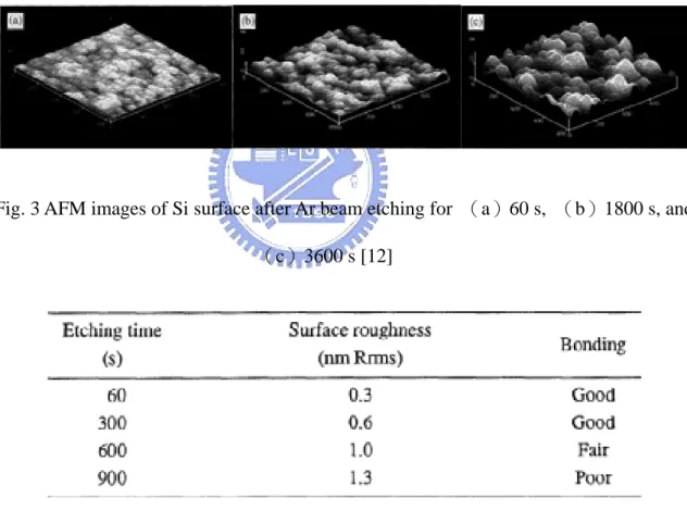
Fig. 3 AFM images of Si surface after Ar beam etching for (a)60 s, (b)1800 s, and(c)3600 s [12] ... 8
Fig. 4 Processes of UV curable adhesive bonding with surface roughness modification... 11
Fig. 5 Topography of the photoresist (a)before RIE (b)after RIE [12]... 13
Fig. 6 Topography of poly-Si after RIE process ... 13
Fig. 7 (a)The design and (b)enlarging view of shell mask ... 14
Fig. 8 Process flows of UV curable adhesive bonding with surface roughness modification... 17
Fig. 9 Processes of modification on surface roughness... 18
Fig. 10 Processes of shell ... 19
Fig. 11 UV curable adhesive bonding setup diagram... 21
Fig. 12 UV curable adhesive bonding processes ... 22
Fig. 13 Image of surface roughness before RIE ... 23
Fig. 14 (a)Side and (b)top view image of surface roughness after RIE... 24
Fig. 15 Profile of wafer (a)without and (b)with surface roughness modification ... 25
Fig. 16 (a)Fabrication results and (b)enlarging view of shell under SEM... 26
Fig. 17 Shell height... 27
Fig. 18 Bonding width of shell(a)4µm (b)2µm... 27
Fig. 19 (a)Bonding result and (b)enlarging view of 2 x 2cm die after dicing operation ... 28
Fig. 20 (a)Result and(b)enlarging view of UV adhesive flow on the interface of silicon wafer and glass under SEM ... 30
Fig. 21 Leakage on the bonding interface ... 31
Fig. 22 Leakage of UV curable adhesive bonding(a)without and(b)with surface roughness modification under O.M. ... 32
Fig. 23 (a)and (b) Setup diagram of bonding strength test ... 35
Fig. 24 Results of bonding strength... 35 Fig. 25 Image and enlarging view of residual UV curable adhesive of die without
surface roughness modification ... 36
Fig. 26 Image and enlarging view of residual UV curable adhesive of die with surface roughness modification ... 37
Fig. 27 Back side of wafer under O.M. ... 38
Fig. 28 Back side profile of wafer ... 39
Fig. 29 Residual Si is produced after RIE process ... 39
List of Tables
Table 1 Comparison of different bonding techniques... 7
Table 2 Measured and interpolated surface roughness related to Ar beam etching time, and bonding results [12] ... 8
Table 3 Processes for modification of the wafer surface and the bonding results... 9
Table 4 Some properties of Pyrex 7740 glass... 16
Table 5 Fabrication parameters of modification on surface roughness ... 18
Table 6 Fabrication parameters of shell... 20
Table 7 Leakage results of different bonding condition ... 33
Chapter 1 Introduction
1.1 Motivation
The MEMS(Micro Electro Mechanical Systems) and NEMS(Nano Electro Mechanical Systems)technologies have evolved to an important field with a great application potential. Combining the knowledge of different fields, including electronics, communication, electro-optical, mechanical, material science, MEMS technology enables us to create different sensing and actuating devices integrated with other microelectronic, and NEMS technology enables us to explore sensors and actuators with very-precise detection and manipulation of objects down to the molecular levels. The MEMS and NEMS devices provide integrated solutions in the incoming decades.
However, there are still many problems to overcome. One of the critical issues for MEMS and NEMS devices commercialization is packaging. Although we can create devices with nano scale by using state-of-the-art technology, there is not a convenient method to package these devices. In addition, these devices often contain structures with moving parts needing shielding from the physical and electrical environments, and require special packaging designs.
Two major challenges today for MEMS and NEMS are packaging cost and packaging size [1]. The most notable issue is cost. MEMS packaging is very expensive and typically accounts for 75% to 95% of the device cost. The reason for such high cost packaging can
only be made based on the high volume markets of these products such like T.I.’s Digital Light Processors, Motorola’s Pressure Sensors, and H.P.’s Ink Print Heads. In smaller markets, a cost-effective and more standardized packaging is necessary for the development of MEMS and NEMS devices. The second issue is packaging size that is usually several times larger than the devices itself. Ideally, packaging components should be in the same scale as the devices. As the NEMS devices are fabricated, the reduction of packaging size can make better space efficiency and higher density in fabrication.
In order to reduce packaging cost and resolve the process complexity of MEMS fabrications, a wafer-level post-process hermetic packaging using UV curable adhesive bonding was introduced for MEMS packaging in 2004 [2]. The UV curable adhesive is cured through UV light exposure without additional heating, suitable for packaging the devices with temperature sensitive materials or processes. However, adhesive bonding by UV curable adhesive has poor bonding strength in nano scale. As the reduction of packaging size, improvement of bonding strength in UV curable adhesive bonding is necessary for NEMS packaging.
1.2 Related Research
1.2.1 NEMS Device
Exploration of NEMS fabrication technologies and applications is an active area of research among engineers and scientists across the globe. Many researchers are investigating the integration of NEMS devices with other systems components. Two NEMS
devices will be introduced in the following sections.
Piezoresistance effect is widely used as a sensing principle by changing resistance when mechanical stresses are applied on the materials. All materials probably have a piezoresistance effect, and it is particularly important in some semiconductors applications. Single crystal silicon is a kind of piezoresistance material. When silicon structure receives an external force, the structure changes its shape and produces stress inside, which indicates resistance change. In 2002, a silicon nano-wire piezoresistor, whose minimum width was 53 nm and thickness was 53 nm, was fabricated by the combination of thermal diffusion, EB (electron beam)direct writing and RIE(reactive ion etching)[3]. Comparing to the
conventional diffused piezoresistor, it has enough sensitivity for mechanical sensor applications.
Fig. 1 (a)AFM and(b)SEM images of Si nano-wire [3]
For another example, we consider a silicon nano-wire biosensor. A SiNW (Boron-doped silicon nanowires)was positioned between two metallic electrodes constituted
the heart of the sensor [4]. The SiNW is chemically functionalized with different binding sites to provide a recognition mechanism for proteins or antibody-antigens. The binding
sites on the wire are specific to the molecule that is targeted for detection. If the target molecule is present in the environment of the SiNW sensor, it will bind to a complementary binding site on the wall of the SiNW. This binding event changes the surface charge density and hence the conductance of the SiNW. The conductance of the SiNW can be monitored electronically and thus, by observing the changes in conductance, the presence of the target molecule can be detected. The SiNW is used to create highly sensitive, real-time electrically based sensors for biological and chemical species [5].
Fig. 2 Operation principle of the SiNW [4]
1.2.2 MEMS Packaging
Packaging is a core technology for the advancement of MEMS. Comparing to the traditional integrated circuit (IC) packaging, MEMS packaging is a more challenging technology, and it presents technical and cost barriers to the widespread realization of multifunctional microsystems. Unlike IC packaging techniques, MEMS packaging is application specific and suffers from a lack of standards [6]. Proper packaging of MEMS
devices is paramount to their success because MEMS devices are extremely sensitive to environmental conditions (i.e. dust, moisture). There are two primary methods used for MEMS packaging [7].
(1)Deposition of some sort of encapsulation layer directly on the device wafer.
(2)Attachment of a cover, usually glass or silicon, on a finished part.
Among various kinds of the wafer packaging techniques where a layer is deposited on the device wafer to provide encapsulation, two approaches can be seen. One is to deposit a sacrificial layer on top of the device layer, deposit the encapsulation layer, then release the structure by etching away the sacrificial layer via access holes in the encapsulation layer, and reseal these access holes [8]. The other is similar except that rather than using access holes to etch away the sacrificial layer, a thin membrane which is permeable to the etch chemistry is used [9].
Several bonding techniques have been used when attaching a cover. Wafer bonding has increasingly become a key technology for materials integration in various areas of MEMS, microelectronics, and optoelectronics. To bond wafers or substrates together, several techniques have been developed. These techniques can be categorized into fusion bonding, anodic bonding, eutectic bonding, solder bonding, and adhesive bonding [10].
Fusion bonding, sometimes calls direct bonding, is usually used to bond bare silicon wafers or oxidized silicon wafers together. Fusion bonding needs cleanliness and flatness of the surface to be bonded and requires a high annealing temperature to achieve reliable bond quality. When annealing in 1000°C or greater, bonding strength of fusion bonding can up to
20 MPa [11].
Anodic bonding is being widely used for bonding glass substrate to other conductive materials due to its good bond quality. Like fusion bonding, anodic bonding requires smooth surface to be bonded. In anodic bonding, the substrates are typically heated to a temperature between 400 and 450 oC. A voltage of 400 to 1200 V is usually applied to the glass and the other substrates to be bonded. Corning 7740, Hoya SD-2, and Schott 8330 are the most frequently used glasses for anodic bonding.
Eutectic bonding, widely used in die bonding, is used to bond two substrates together at eutectic temperature by taking the advantage of solid solubility of silicon and other materials. The most common material used in eutectic bonding is gold. Au-Si eutectic bonding, involves a process temperature higher than the Au-Si eutectic temperature of 363 oC. When glass layers are used for bonding, the firing temperature has to be above 400 oC. A higher process temperature is still involved in eutectic bonding and glass frit bonding [10].
Solder bonding utilizes alloys with low melting point to bonding two different surfaces together. With sufficient heating, these alloys melt into liquid and join two different substrates together. It can reduce the bonding temperature and has been employed for many applications. Sn based alloys and Al are the most common material for solder bonding.
Adhesive bonding utilizes epoxy or photoresist to bond two substrates. These polymers are applied to the substrate through spin coating, and then patterns are defined by ordinary exposure and development process. With proper heat treatment and pressure, polymer is cured and forms strong bonds between two substrates. Normally, adhesive bonding can be
performed under much lower temperature than most bonding procedures, often below 300°C [2]. In 2004, a low temperature wafer-level hermetic packaging in micro scale by using UV adhesive was proposed. This process needs no heating, eliminates all of the drawbacks induced by heat. This feature is especially welcome for temperature sensitive materials.
Bonding
Technique Application Advantage Drawback
Processing Temperature
Fusion Si, oxidized Si Over 1000°C
Anodic Glass to other
conductive materials Hermetic, Strong Bonding Surface Roughness Sensitive 300-500°C Eutectic
Bond two substrates at eutectic temperature
Strong Bonding Flat, clean surface required
363°C (Au-Si)
Solder Utilize alloys with low melting point
Hermetic, Strong Bonding
Solder flow
possible 180~400°C
Adhesive Utilize epoxy or
photoresist Low Temp.
Poor long term
reliability 130~300°C UV Adhesive Utilize UV curable adhesive Room Temp. Rough surface Poor bonding strength 25~30°C
Table 1 Comparison of different bonding techniques
1.2.3 Surface Roughness
By presence of intermediate layer, wafer bonding techniques can be classified into two main groups, non-intermediate layer boning and intermediate layer bonding. Non-intermediate layer boning like fusion and anodic bonding has advantage of hermetic and
strong bonding. However, wafer surface to be bonded must be well polished and completely particle free. The surface roughness of wafer becomes a key parameter in wafer bonding.
In 1998, the effect of surface roughness in fusion bonding by Ar beam surface activation was proposed [12]. The surface roughness of wafer is enhanced by Ar beam etching of different etching time. The AFM images of Si surface after Ar beam etching are shown in Fig. 3. The bonding results show that high surface roughness degrades bonding strength and results in void formation.
Fig. 3 AFM images of Si surface after Ar beam etching for (a)60 s, (b)1800 s, and (c)3600 s [12]
Table 2 Measured and interpolated surface roughness related to Ar beam etching time, and bonding results [12]
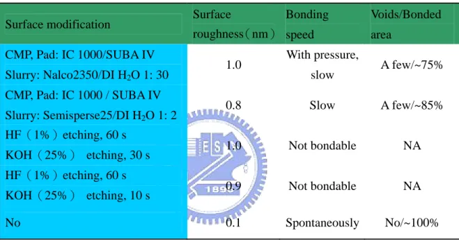
Here is another example. The effect of surface roughness of different process on direct wafer bonding was proposed in 1999 [13]. Using CMP and chemical etching, wafer surfaces
are modified such that they have surface roughness difference. The processes for modification of the wafer surface and the results of fusion bonding are shown in table 3. Correlation between the surface roughness and bonding is clear. Wafer which has the lowest surface roughness bonds spontaneously. Wafers after HF and KOH etching were not bondable at all, even under pressure. Wafers after CMP process bonded slowly, and there are a few voids that are visible by means of the IR camera.
Surface modification Surface
roughness(nm) Bonding speed Voids/Bonded area CMP, Pad: IC 1000/SUBA IV Slurry: Nalco2350/DI H2O 1: 30 1.0 With pressure, slow A few/~75% CMP, Pad: IC 1000 / SUBA IV Slurry: Semisperse25/DI H2O 1: 2 0.8 Slow A few/~85% HF(1%)etching, 60 s
KOH(25%) etching, 30 s 1.0 Not bondable NA
HF(1%)etching, 60 s
KOH(25%) etching, 10 s 0.9 Not bondable NA
No 0.1 Spontaneously No/~100%
Table 3 Processes for modification of the wafer surface and the bonding results
1.3 Present Approach
As we mentioned in the related research, there are two primary methods used for MEMS packaging. We choose the method of a separate lid for several reasons. It resolves the process complexity and lower packaging cost.
However, surface roughness of wafer is easily modified by processes such as CMP or chemical etching. As the reduction of packaging size, it is difficult to make a flat and clean surface especially in nano scale for fusion, anodic, and eutectic bonding. We can recognize from what has been said above that wafer with nano surface roughness makes bonding more difficult. In addition, high temperature process is unsuitable in many applications.
Using UV curable adhesive to bond can solve these problems. A low temperature wafer-level hermetic packaging in micro scale by using UV curable adhesive was demonstrated in 2004. However, adhesive bonding by using UV curable adhesive has poor bonding strength in nano scale. It is clear that the surface roughness is a key parameter in wafer bonding. In the last few years, several articles have been devoted to the study of the effect of surface roughness on non-intermediate layer bonding, but only few attempts have so far been made at the effect of surface roughness on intermediate layer bonding.
Here, surface roughness modification will be proposed for the improvement of UV adhesive bonding strength. It increases adhesive contact area and enhances adhesive bonding strength by the combination of lithography, dry oxidation, and RIE etching. Moreover, curing process can be done in seconds by increasing UV light intensity. It is expected that fast, high bonding strength, and low temperature process packaging by using UV curable adhesive with surface roughness modification can provide a convenient approach for MEMS and NEMS packaging.
Chapter 2 Concept Design
2.1 UV Adhesive Bonding with Surface Roughness Modification
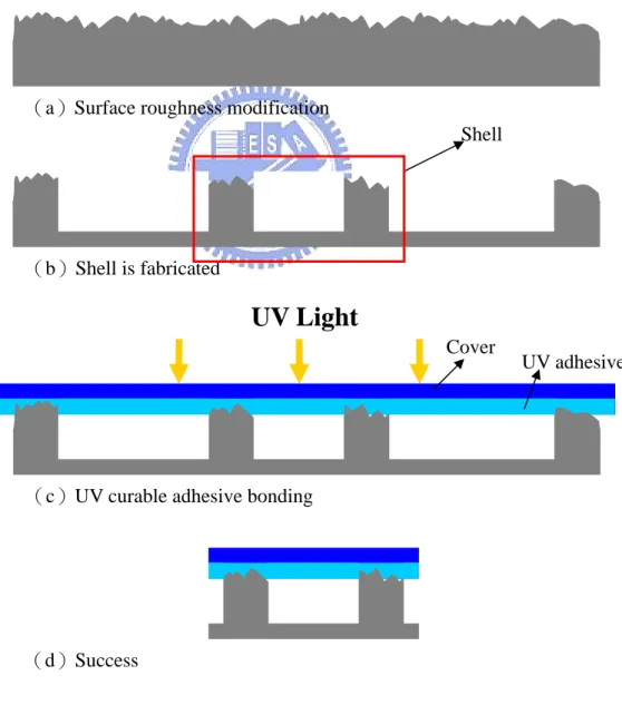
The main concept of adhesive bonding with surface roughness modification is shown as Fig. 4. There are four major elements of this packaging process, surface roughness, shell, UV curable adhesive, and cover. Each of them will be discussed in the following sections.
Fig. 4 Processes of UV curable adhesive bonding with surface roughness modification (a)Surface roughness modification
(b)Shell is fabricated
(c)UV curable adhesive bonding
UV Light
Cover
UV adhesive Shell
2.2 Surface Roughness Modification
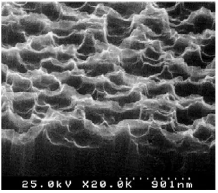
A method on surface roughness modification by combining spin-on photoresist, RIE, and wet etching was proposed in 2003 [12]. The principle is based on an uneven etch of the photoresist by RIE, where the photoresist acts as the transferring template. Therefore part of the underneath material will be exposed and be etched according to the uneven photoresist template. The roughness of the underneath material is then modified after the proper etch.
Fig. 5(a)and(b)show the SEM image of the photoresist before and after the RIE process, respectively. Before RIE, the surface of the photoresist is very smooth. After RIE, the surface of the photoresist has been roughened by the etching, and a lot of pinholes can be observed, as shown in Fig. 5(b). At this point the target material is not yet revealed and still protected by photoresist. With longer etching time, the target surface underneath the pinhole region is then attacked by the RIE, and the attacked area of the target surface will grow with the increasing pinhole region of the photoresist. Therefore, the rough topography of photoresist is transferred into the target material due to this time difference [12]. Fig. 6 shows the modification of surface roughness after RIE process.
Fig. 5 Topography of the photoresist (a)before RIE (b)after RIE [12]
Fig. 6 Topography of poly-Si after RIE process
2.3 The Design of Shell
Shell is utilized to estimate the bonding result and designed by several reasons.
(1)Reduction of common packaging size in micro scale
(2)Fabrication and measurement are convenient in lab instruments
(3)The shell height is enough to ensure UV adhesive curing on the top face of shell
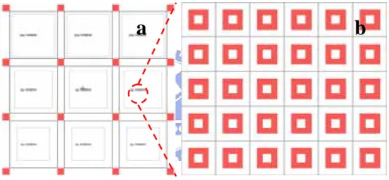
Fig. 7 shows the design and enlarging view of shell mask. 500 x 500 shells are fabricated in 2 x 2 cm die. The small square areas are used for the alignment of dicing and measurement of surface roughness.
Fig. 7 (a)The design and (b)enlarging view of shell mask
2.4 The Selection of UV curable Adhesive
UV curable adhesive is widely used in many applications. Different kinds of UV adhesive have been developed for different purposes. However, there are no UV curable adhesive used for glass/silicon wafer bonding, we choose suitable UV curable adhesive from commercial products. The selection is based on the following criteria:
(1)Low viscosity for spin coating and pattern gap flowing
(2)Good adhesion between glass to silicon wafer
(3)High bonding strength
(4)Single component for easier use
UV curable adhesive is provided by Henkel, Taiwan. LOCTITE○R product 3491 is recommended because it is a low viscosity, single component, designed for bonding glass to itself and to a variety of other surfaces. Product 3491 also exhibits excellent resistance to prolonged humidity or water immersion [15].
2.5 The Selection of Cover
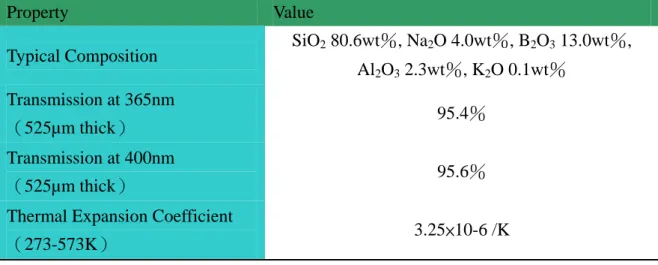
UV curable adhesive is cured by UV light exposure with correct wave length and sufficient dosage. Due to this reason, the cover has to be transparent to UV light. Corning Pyrex 7740, Hoya SD-2, and Schott 8330 are the most frequently used glasses for bonding. Corning Pyrex 7740 glass is chosen since it is transparent to UV light, mechanically robust, and shows good resistance to various chemicals. Moreover, Pyrex 7740 glass has close CTE (Coefficient of Thermal Expansion) to single crystal silicon. In high temperature accelerated test, this characteristic could minimize possible residual thermal stress at the silicon/glass interface and reduce the variables in the experiment.
Property Value
Typical Composition SiO2 80.6wt%, Na2O 4.0wt%, B2O3 13.0wt%,
Al2O3 2.3wt%, K2O 0.1wt%
Transmission at 365nm
(525µm thick) 95.4%
Transmission at 400nm
(525µm thick) 95.6%
Thermal Expansion Coefficient
(273-573K) 3.25×10⁻⁶ /K
Chapter 3 Fabrication and Bonding
3.1 Process Flow
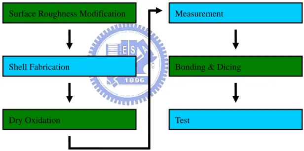
The main processes of UV curable adhesive bonding with surface roughness modification are shown in Fig. 8. The detailed parameters are described in the following sections.
Fig. 8 Process flows of UV curable adhesive bonding with surface roughness modification
3.2 Surface Roughness Modification
The principle is based on an uneven etch of the photoresist by RIE, where the photoresist acts as the transferring template. Therefore part of the underneath material will be exposed
Surface Roughness Modification
Shell Fabrication
Dry Oxidation
Measurement
Bonding & Dicing
and be etched according to the uneven photoresist template. The roughness of the underneath material is then modified after the proper etch. The processes of modification on surface roughness are shown in Fig. 9. The fabrication parameters of modification on surface roughness are shown in table 5.
Fig. 9 Processes of modification on surface roughness
Step Process
Photoresist spin 0.5 µm FH-6400 spin and bake at 120°C for 5min
RIE SF6:O2=20:4 sccm. at 20mTorr and rf =100W
Removal of residual resist H2SO4:H2O2 = 3:1 with hot bath for 15min
FH-6400 Silicon wafer
(a)Spinning 0.5 µm FH-6400 on Si wafer
(b)Etching FH-6400 and Si wafer by RIE
(c)Removing residual photoresist
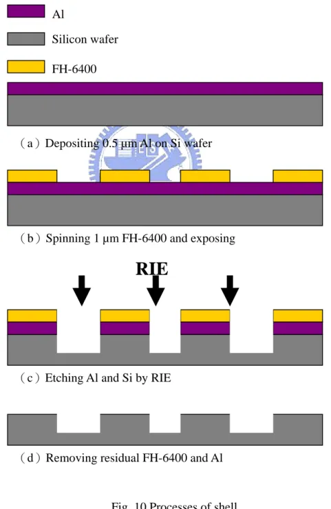
3.3 Shell
Al is deposited as mask layer to prevent Si form etching by RIE. Then photoresist is deposited and patterned. Pattern on photoresist is transferred to Al and Si after RIE etching. Fig. 10 shows the processes of shell. Fabrication parameters of shell are shown in table 6.
Fig. 10 Processes of shell
RIE
FH-6400 Silicon wafer
(b)Spinning 1 µm FH-6400 and exposing
(c)Etching Al and Si by RIE
(d)Removing residual FH-6400 and Al (a)Depositing 0.5 µm Al on Si wafer
Step Process
Mask layer deposition 0.5 µm Al deposit
Lithography 1µm FH-6400 spin and exposure for 0.5s
RIE Si etch for 7min
Removal of Al HCl:H2O = 1:1 with hot bath for 20min
Table 6 Fabrication parameters of shell
3.4 Bonding
Due to the reason that UV curable adhesive can not be soft baked. UV curable adhesive remains in liquid phase in the whole bonding process. Contact-separate-align techniques which usually use in conventional contact aligner can not be adopted directly in the UV curable adhesive bonding and need modification. Since there is no special equipment which designs for UV curable adhesive bonding, mask is used for fixing the glass. After spinning UV curable adhesive, glass wafer is fixed on the mask by tape. Then mask holder sucks mask by vacuum. The UV curable adhesive bonding setup diagram and processes are shown respectively in Fig. 11 and Fig. 12.
Fig. 11 UV curable adhesive bonding setup diagram
Mask holder
Mask
Wafer stage
Die
(b)Wafer stage rises up and contacts with mask
(a)Side view of contact aligner after mask holder face down Glass Wafer
Mask
Tape
(d)UV curable adhesive is spun on glass wafer
(e)Glass wafer with UV adhesive is fixed on mask Glass UV adhesive
(f)Glass and Si die are contact and UV light flood exposure to cure the adhesive
(g)UV curable adhesive bonding is finished Mercury lamp
(c)The level of wafer stage is fixed by vacuum and wafer stage descends
Chapter 4 Results and Discussion
4.1 Surface Roughness
It is clear that surface roughness of wafer is successfully modified by RIE from Fig. 13 and Fig. 14. Then surface profiler is used to measure the surface roughness of wafer. The measurement results of surface roughness before and after RIE are shown in Fig. 15. The Ra of wafer with and without surface roughness modification is about 0.4nm and 12.4nm respectively.
Fig. 14 (a)Side and (b)top view image of surface roughness after RIE
b
a
Fig. 15 Profile of wafer (a)without and (b)with surface roughness modification
a
4.2 Shell
Fig. 16 (a)Fabrication results and (b)enlarging view of shell under SEM
a
SEM(Scanning Electron Microscopy) is used to measure the fabrication result. Fig.17 shows the shell height is about 9µm. Fig. 18 shows the bonding width of shell is 4µm and 2µm respectively.
Fig. 17 Shell height
Fig. 18 Bonding width of shell(a)4µm (b)2µm
4.3 Bonding Result
Fig. 19 (a)Bonding result and (b)enlarging view of 2 x 2cm die after dicing operation
b
a
4.4 Measurement Results
There are three kinds of test used to examine the performance of UV curable adhesive bonding with surface roughness modification, UV curable adhesive, leakage, and bonding strength. Each of them will be discussed in the following sections.
4.4.1 UV Curable Adhesive
After bonding process, dicing operation is used to inspect the condition of UV curable adhesive flow on the interface of silicon wafer and glass. Die is cut and then examined under SEM. Fig. 20 shows the result and enlarging view of UV curable adhesive flow. Obviously, the shell height is enough to prevent UV curable adhesive from curing on the bottom face of shell. There are other things to note. Since UV curable adhesive remains in liquid phase, it flows between shells and covers the lateral area of shells. UV curable adhesive is spun about 2.5µm before bonding. From Fig. 20(b), the shell height covered by UV curable adhesive is about 1.5µm after bonding.
Fig. 20 (a)Result and(b)enlarging view of UV adhesive flow on the interface of silicon wafer and glass under SEM
a
4.4.2 Leakage
During bonding process, leakage occurs on the bonding interface as shown in Fig. 21. This phenomenon occurred during the contact step of bonding process and may due to:
1. The reflow of UV curable adhesive
2. Poor flatness in fixing glass wafer on mask
3. Uneven wafer stage
These problems may be solved by the improvement of bonding tool, such as bonding equipment or nano imprinting technique.
To estimate the bonding leakage, die is put into water for 15 seconds and observed through optical microscope. The residual water on the bonding interface changes the reflected color under optical microscope. The leakage can be observed form Fig. 22.
Fig. 22 Leakage of UV curable adhesive bonding(a)without and(b)with surface
b
a
The leakage results of different bonding condition are shown in table 7. This table indicates that larger bonding width or bonding with higher surface roughness have less leakage. The leakage is reduced 9% to 14% by increasing bonding width and 3% to 8% by increasing surface roughness. Larger bonding area and higher surface roughness on bonding interface are two keys in reducing leakage.
Bonding Width Ra Leakage
2µm 24.3% 4µm 0.4 nm 10.8% 2µm 16.8% 4µm 12.4nm 7.7%
Table 7 Leakage results of different bonding condition
4.4.3 Bonding Strength
Bonding strength test is necessary to demonstrate the performance of UV curable adhesive with surface roughness modification. The size of test die is 1 x 1cm. As shown in Fig. 23, the top and bottom of die are attached to connect pads with glue, and pull gate is attached to connect pads and used to measure the bonding strength. The results of bonding strength are shown in Fig. 24. This figure indicates:
1. At the same surface roughness, larger bonding width has larger bonding force.
bonding force.
3. As the bonding width increases, the contribution of surface roughness modification for bonding force increases.
After calculation, the total bonding area of 2µm and 4µm bonding width is 14.41mm2 and 23.53mm2 respectively and bonding strength is shown in table 8. Obviously, UV curable adhesive bonding with higher surface roughness has larger bonding force. The bonding strength is enhanced 34.6% in 2µm bonding width and 43.2% in 4µm bonding width. There are other things to note, the bonding contribution of 1.5µm lateral area is included in calculation. In order to eliminate the lateral contribution, Si wafer without shells and surface roughness modification is bonded to glass wafer and the bonding strength is 7.29MPa. The bonding strength of wafer with shells is also enhanced by the surface roughness modification of lateral area.
In addition, residual UV curable adhesive is examined under SEM after bonding strength test. Fig. 25 and Fig. 26 show the residual UV curable adhesive of die with and without surface roughness modification respectively. These figures indicate that residual UV curable adhesive of die with surface roughness modification is widely covered and thicker. In other words, wafer with surface roughness modification has better adhesion toward UV curable adhesive.
Fig. 23 (a)and (b) Setup diagram of bonding strength test
Fig. 24 Results of bonding strength
Bonding Width Ra Bonding Strength(MPa)
2µm 9.02 4µm 0.4 nm 9.41 2µm 12.14 4µm 12.4 nm 13.48
Table 8 Bonding strength
die
b
a
Fig. 25 Image and enlarging view of residual UV curable adhesive of die without surface roughness modification
b
a
Fig. 26 Image and enlarging view of residual UV curable adhesive of die with surface roughness modification
b
a
4.5 Discussion
The back side of wafer surface is used to experiment and show high surface roughness is unsuitable in nano packaging application. The back side of wafer surface is unpolished and shown in Fig. 27. The Ra is 0.6µm and surface profile is shown in Fig. 28. Such high surface roughness makes uneven thickness of photoresist in spinning FH-6400. After lithography process, the residual photoresist is observed on wafer surface. During RIE process, the residual photoresist becomes masking layer and produces residual Si as shown in Fig. 29. Fig. 30 shows the 3D view and surface profile of wafer. The white areas in Fig. 30(a) are residual Si. Such high surface roughness is unsuitable to integrate in fabrication processes.
Fig. 28 Back side profile of wafer
Fig. 30 (a)3D view and (b)surface profile of wafer
a
b
Residual Si Measurement path
4.6 Conclusion
UV curable adhesive bonding with surface roughness modification is achieved to enhance bonding strength, reduce leakage, and decrease bonding temperature to room temperature. In addition, curing process can be done in seconds by increasing UV light intensity. This method may especially welcome for NEMS device packaging. By using nano imprinting technique like micro contact printing or hot embossing, UV curable adhesive can be transferred to bonding surface of nano width, and transparent plastic cap such as polycarbonate can be utilized as protection cap. It is expected that fast, high bonding strength, and low temperature process packaging by using UV curable adhesive with surface roughness modification can provide a convenient approach for MEMS and NEMS packaging. In addition, the back side of wafer surface is used to experiment and show high surface roughness is unsuitable in nano packaging application. The Ra 0.6µm generates residual photoresist and makes fabrication fail during lithography process. Such high surface roughness is unsuitable to integrate in fabrication processes.
Acknowledgement
The operation of RIE process is supported by National Chiao-Tung University Nano
Facility Center (Semiconductor Research Center) with assistance by Hsiu-Luan Hsu.
UV curable adhesive is provided by Henkel, Taiwan, Ltd. with technical assistance
Reference
[1] A.P. De Silva, and H.G. Hughes, “The package integration of RF-MEMS switch and control IC for wireless applications”, Advanced Packaging, IEEE Transactions on, vol. 26, pp.255-260, Aug, 2003.
[2] Z.H. Liang, Y.T. Cheng, W.S. Hsu, and Y.W. Lee, “A low temperature wafer-level hermetic MEMS package using UV curable adhesive”, Electronic Components and Technology, 2004. ECTC '04. Proceedings, vol. 2, pp. 1486-1491, 1-4 June, 2004. [3] T. Toriyama, Y. Tanimoto, and S. Sugiyama, “Single crystal silicon nano-wire
piezoresistors for mechanical sensors”, Microelectromechanical Systems, Journal of, vol. 11, pp. 605-611, Oct, 2002.
[4] Y.C. Lee, B. Amir Parviz, J.A. Chiou, and Shaochen Chen, “Packaging for
microelectromechanical and nanoelectromechanical systems” Advanced Packaging, IEEE Transactions on, vol. 26, pp. 217-226, Aug, 2003.
[5] Y. Cui, Q.Q. Wei, H.K. Park, and C.M. Lieber, “Nanowire nanosensors for highly sensitive and selective detection of biological and chemical species”, Science, vol. 293, pp. 1289-1292, 2001.
[6] Yi Tao, A.P. Malshe, W.D. Brown, D.R. DeReus, and S. Cunningham, “Laser-assisted sealing and testing for ceramic packaging of MEMS devices”, Advanced Packaging, IEEE Transactions on, vol. 26, pp. 283-288, Aug, 2003.
[7] R.N. Candler, W.T. Park, Huimou Li, G. Yama, A. Partridge, M. Lutz, and T.W. Kenn, “Single wafer encapsulation of MEMS devices”, Advanced Packaging, IEEE
Transactions on, vol.26, pp. 227-232, Aug, 2003.
Kenny, “Wafer-scale film encapsulation of micromachined accelerometers”, Transducers, Solid-State Sensors, Actuators and Microsystems, 12th International Conference on, vol. 2, pp. 1903-1906, June, 2003.
[9] K.S. Lebouitz, A. Mazaheri, R.T. Howe, and A.P. Pisano, “Vacuum encapsulation of resonant devices using permeable polysilicon”, Micro Electro Mechanical Systems, MEMS '99. Twelfth IEEE International Conference on, pp. 470-475, Jan, 1999.
[10] Jun Wei, S.M.L. Nai, C.K.S. Wong, Zheng Sun, and Loke Chong Lee, “Low temperature glass-to-glass wafer bonding”, Advanced Packaging, IEEE Transactions on, volume. 26, pp. 289-294, Aug, 2003.
[11] P.W. Barth, “Silicon fusion bonding for fabrication of sensors, actuators, and microstructures”, Sensors and Actuators, A21-23, pp. 919-926, 1990.
[12] Hideki Takagi, Ryutaro Maeda, Teak Ryong Chung, Naoe Hosoda, and Tadatomo Suga, “Effect of surface roughness on room-temperature wafer bonding by Ar beam surface activation”, Jpn. J. Appl. Phys. vol. 37, pp. 4197-4203, 1998.
[13] C. Gui, M. Elwenspoek, N. Tas, and J.G.E. Gardeniers, “ The effect of surface roughness on direct wafer bonding”, Journal of Applied Physics, vol. 85, pp. 7448-7455, May, 1999. [14] C.C. Lee, and W.S. Hsu, “Method on surface roughness modification to alleviate stiction
of microstructures”, Journal of Vacuum Science & Technology B, vol. 21, pp.1505-1510, July, 2003.
![Fig. 1 (a)AFM and(b)SEM images of Si nano-wire [3]](https://thumb-ap.123doks.com/thumbv2/9libinfo/8717395.200323/13.892.164.791.532.876/fig-afm-b-sem-images-si-nano-wire.webp)
![Fig. 2 Operation principle of the SiNW [4]](https://thumb-ap.123doks.com/thumbv2/9libinfo/8717395.200323/14.892.305.678.469.720/fig-operation-principle-sinw.webp)