國 立 交 通 大 學
電子工程學系 電子研究所碩士班
碩士論文
複晶矽薄膜電晶體之製程與可靠度之研究
Study on the Process and Reliability of Poly-Si
Thin-Film Transistors
研 究 生:桑任逸
指導教授:雷添福 博士
複晶矽薄膜電晶體之製程與可靠度之研究
Study on the Process and Reliability of Poly-Si
Thin-Film Transistors
研 究 生:桑任逸 Student: Jen-Yi Sang 指導教授:雷添福 博士 Advisor: Dr. Tan-Fu Lei
國 立 交 通 大 學
電子工程學系 電子研究所碩士班
碩士論文
A Thesis
Submitted to Department of Electronics Engineering & Institute of Electronics College of Electrical Engineering and Computer Science
National Chiao Tung University In Partial Fulfillment of the Requirements
For the Degree of Master of Science
in
Electronic Engineering June 2005
Hsinchu Taiwan Republic of China
複晶矽薄膜電晶體之製程與可靠度之研究
學生: 桑任逸
指導教授: 雷添福 博士
國立交通大學
電子工程學系 電子研究所碩士班
摘 要
在本論文中,首先,我們提出在摻氟矽玻璃(FSG)上製造的複晶矽薄膜電晶 體。實驗結果顯示元件的電特性和均勻度可藉由摻雜適量的氟原子達到明顯的改 善。與傳統複晶矽薄膜電晶體相較之下,製造在摻氟矽玻璃上的複晶矽薄膜電晶 體具有較高的導通電流及場效遷移率,並使得漏電流降低。這是因為氟原子能修 補複晶矽與絕緣層介面處及位於通道中複晶矽晶格邊界的缺陷。再者,由於氟與矽原子可形成較強的鍵結,經過熱載子應力(hot carrier stress)測試後,發現摻入
氟原子的複晶矽薄膜電晶體具有較好的可靠度。
接著,我們進行有關多重通道(multi-channel)複晶矽薄膜電晶體的研究。藉
由增加通道的數目來提高閘極的控制能力,可以改善元件的電特性;包括提高導
通電流,降低臨界電壓(threshold voltage)及次臨限擺幅(subthreshold swing)。然
而,元件的可靠度卻會因此而變差。我們推測是由於在多重通道的結構中,靠近
汲極端的電場強度會增加,而導致更嚴重的碰撞游離(impact ionization)所造成。
最後,我們探討有關複晶矽薄膜電晶體生命週期(lifetime)的問題。發現到最
閘極電壓等於二分之一汲極電壓。此外,亦發現到在高的汲極電壓(drain voltage)
應力測試條件下,導通電流隨時間的劣化具有相同的斜率,生命週期的分佈亦呈
線性關係,因為在此情形下元件的傷害主要是由碰撞游離(impact ionization)所造
成。然而,在低的汲極電壓(drain voltage)測試條件下會有不同的現象發生。這是
因為此時必須考慮寄生雙極性接面電晶體效應(parasitic bipolar junction transistor
Study on the Process and Reliability of Poly-Si
Thin-Film Transistors
Student: Jen-Yi Sang
Advisor: Dr. Tan-Fu Lei
Department of Electronics Engineering &
Institute of Electronics
National Chiao Tung University
ABSTRACT
In this thesis, first, a process-compatible scheme for fabricating poly-Si TFTs on
an FSG buffer layer was proposed and demonstrated. Experimental results reveal that
remarkably improved device performance and uniformity can be achieved with
appropriate fluorine concentration. The poly-Si TFT fabricated on FSG layers has a
higher on-current, a lower leakage current, and a higher field-effect mobility
compared with the conventional poly-Si TFT. The fluorine atoms can passivate the
Si/SiO2 interface states and grain boundary trap states in the poly-Si. Furthermore, the
incorporation of fluorine also increases the reliability of poly-Si TFTs against hot
carrier stressing, which is attributed to due to the formation of the rather strong Si-F
bonds.
Then, Multi-channel poly-Si TFTs were studied. The device’s electrical
characteristic such as on-current, threshold voltage, and subthreshold swing were
improved with increasing the channel stripes due to the enhancement of gate control
electric field strength near the drain side was enlarged in multi-channel structure,
causing severer impact ionization.
Finally, we studied the lifetime issue of poly-Si TFTs. It was found that the
worst-case of stress conditions is under VG≈Vth, not VG=1/2 VD. Moreover, it is
revealed that under high VD of stress conditions, the Ion degradation has the same
slope with stress time and the lifetime distribution has a linear relationship due to
impact ionization dominating. However, under low VD, it shows a different
phenomenon. We concluded that the parasitic BJT should be considered in these stress
誌謝
首先向指導教授雷添福博士至上無限的謝意,在老師的細心指導下,本論文 得以順利完成。兩年的研究生涯中,不僅僅只是學習到做研究的精神與方法,老 師的關心、鼓勵與啟發,使我在面對將來漫長的人生旅途,受用無窮。 再者,我要特別感謝王獻德學長與謝明山學長,學長在研究過程中都很熱心 地幫助我、指導我。尤其是在我徬徨無助、沮喪的時候,適時的拉我一把,讓我 能繼續堅持下去。另外還有實驗室的李名鎮學長、王哲麒學長、李宗霖學長、郭 柏儀學長、小強學長、建豪學長、楊紹明學長、小賢學長,感謝你們這些日子以 來的關心與指導。也要感謝志仰、家文、仁杰、柏浩、源竣、俊嘉、宗元、梓祥、 統億、錦石,懷念與你們相處的日子以及一起討論課業時的那股求知的熱情。 最後,我要向我的父母桑鶴年先生與陳愛錦女士致上我最深的感謝,感謝他 們無怨無悔的犧牲奉獻,含莘茹苦將我拉拔長大,並且當我因受挫折而徬徨時引 領我扶持我繼續向前,沒有你們的支持與鼓勵就不會有現在的我,僅以此論文獻 予你們。Contents
Abstract (Chinese) ………I
Abstract (English) ………..III
Acknowledge ………V
Contents ………..VI
Table & Figure Captions .………...VIII
Chapter 1 Introduction ……….1
1.1 Overview of Poly-Si Thin-Film Transistors ....………...1
1.2 Motivation ……….………..……...2
1.2.1 Passivation of Trap State ...………2
1.2.2 Multiple Channel ………...…4
1.2.3 Lifetime ………….………5
1.3 Organization of the Thesis………..6
References ………8
Chapter 2 Characteristics of Low Temperature Poly-Si TFTs on FSG Buffer Layer………....…....……….………...14
2.1 Introduction ……….………...…..14
2.2 Experimental …...………..………...………..15
2.3 Method of Device Parameter Extraction ………..…………17
2.3.1 Determination of Threshold Voltage ………...17
2.3.2 Determination of Subthreshold-Swing .………..….18
2.3.3 Determination of Field Effect Mobility..………...19
2.3.4 Determination of ON/OFF Current Ratio .……….….…....19
2.4 Results and discussion………..21
2.4.1 Characteristics of Poly-Si TFTs on FSG Layer ………...……..…..21
2.4.2 Uniformity and Reliability of Poly-Si TFTs on FSG Layer ……..……..23
2.5 Summary ……….……….…25
References ………..………26
Chapter 3 Electrical Characteristics and Reliability of Multi-Channel Poly-Si TFTs ………...………..43
3.1 Introduction ………..43
3.2 Experimental ………..………..44
3.3 Results and Discussion ……….45
3.3.1 Characteristics of Poly-Si TFTs with Multiple Channels 0………45
3.3.2 Reliability of Poly-Si TFTs with Multiple Channels……….………...47
3.4 Summary ………...………...49
References ……….……….50
Chapter 4 The Lifetime of Poly-Si Thin-Film Transistors …………...…..…...69
4.1 Introducion ……….………..69
4.2 Experimental …...……….………70
4.3 Results and Discussion ……….71
4.4 Summary ...………...75
References ……..………76
TABLE CAPTIONS
Chapter 2
Table 2-1 Summary of different deposition conditions of FSG buffer layer
Table 2-2 Summary of device parameters of the conventional and the proposed
poly-Si TFTs (W/L = 40μm/10μm) with different FSG layer deposition
conditions.
Chapter 3
Table 3-1 Summary of the dimensions of S1, M4, M8, M20, and M40 TFTs. All
devices have the same active channel thickness 100nm, gate TEOS-oxide
thickness 50nm, and total channel width 40μm.
Table 3-2 Summary of device parameters of the conventional and the proposed
multi-channel poly-Si TFTs (W/L = 40μm/2μm) with different stripes of
FIGURE CAPTIONS
Chapter 2
Fig. 2-1 Process flow of the proposed poly-Si TFTs on a FSG buffer layer.
Fig. 2-2 SIMS profiles of the FSG layer as-deposited samples with different FSG
layer deposition conditions.
Fig. 2-3 Transfer characteristics of the conventional and the proposed poly-Si TFTs
with different FSG layer deposition conditions.
Fig. 2-4 Field effect mobility of the conventional and the proposed poly-Si TFTs
with different FSG layer deposition conditions.
Fig. 2-5 SIMS profiles of the conventional and the proposed poly-Si TFTs with
different FSG layer deposition conditions.
Fig. 2-6 Trap state density extraction of the conventional and the proposed poly-Si
TFTs with different FSG layer deposition conditions.
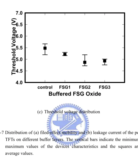
Fig. 2-7 Distribution of (a) filed-effect mobility and (b) leakage current of the
poly-Si TFTs on different buffer layers. The vertical bars indicate the
minimum and maximum values of the devices characteristics and the
squares are the average values.
Fig. 2-8 (a) on-current, (b) threshold voltage, and (c) field effect mobility
degradation as a function of stress time under hot-carrier stress.
Chapter 3
Fig. 3-1 Process flow of the conventional and multi-channel poly-Si TFTs.
Fig. 3-2 Cross-section of the conventional and multi-channel poly-Si TFTs is
Fig. 3-3 Cross-section of the conventional and multi-channel poly-Si TFTs is
perpendicular to the direction of the source and drain electrode.
Fig. 3-4 Top view of the conventional and multi-channel poly-Si TFTs in (a), (b),
(c), and (d). (The effective channel width Weff = 40μm ; channel length L
= 2μm.)
Fig. 3-5 Transfer characteristics of the conventional and the proposed multi-channel
poly-Si TFTs with different stripes of channel.
Fig. 3-6 Field effect mobility of the conventional and the proposed multi-channel
poly-Si TFTs with different stripes of channel.
Fig. 3-7 Trap state density extraction of the conventional and the proposed
multi-channel poly-Si TFTs with different stripes of channel.
Fig. 3-8 Increasing ratio of the effective channel width and the on-state current as a
function of number of channel stripes.
Fig. 3-9 Output characteristics of the conventional and the proposed poly-Si TFTs
with different stripes of channel. (VG – Vth = 0.5; 2; 3.5V)
Fig. 3-10 (a) on-state current, (b) field effect mobility, and (c) threshold voltage as a
function of different gate length with the number of channel stripes.
Fig. 3-11 (a) on-current, and (b) threshold voltage degradation as a function of stress
time under hot-carrier stress.
Fig. 3-12 Trap state density (Nt), before and after 4sec, 10sec, and 100sec stress with
different number of channel stripes.
Fig. 3-13 Increasing ratio of trap state density after 4sec, 10sec, and 100sec stress
with different number of channel stripes.
Fig. 3-14 Schematic plot of structures for simulation.
Fig. 3-15 Electric field distribution in the poly-Si channel of dual-gate TFTs.
Chapter 4
Fig. 4-1 Process flow of the conventional poly-Si TFTs.
Fig. 4-2 Cross-section of the conventional poly-Si TFTs.
Fig. 4-3 Transfer characteristics of the conventional poly-Si TFTs.
Fig. 4-4 On-current variations under stress conditions of VG=1/2 VD and VG=Vth
under VDS=20V and 18V.
Fig. 4-5 On-current variations as a function of stress time with stress drain voltage
(VDS) as a parameter.
Fig. 4-6 Lifetime as function of the reciprocal drain voltage stress for poly-Si TFTs
stressed at VGS≈Vth with VDS from 10 to 20V.
Fig. 4-7 Magnitude of device degradation (A) as a function of drain voltage VDS.
Fig. 4-8 Schematical plot of the occurrence of impact ionization and bipolar
Chapter 1
Introduction
1.1
Overview of Poly-Si Thin-Film Transistors
In 1966, the first polycrystalline silicon thin film transistors (Poly-Si TFTs) were fabricated by C. H. Fa et al. [1]. So far, numerous research reports have been proposed to study the conduction mechanism, fabrication processes and device structures of the poly-Si TFTs in order to enhance the device performance. However, the research in poly-Si TFTs fabrication with temperature below 600°C was not commenced until 1980s. In the past twenty years, low-temperature polysilicon (LTPS) TFTs have been widely investigated in industrial applications, such as active-matrix liquid-crystal displays (AMLCDs) [2-4], high density static random access memories (SRAMs) [5], electrical erasable programming read only memories (EEPROM) [6][7] and candidate for 3-D ICs’ applications [8], etc. Within those applications, the application of active-matrix liquid-crystal displays (AMLCDs) is the major driving force to promote the developments of poly-Si TFT technology.
It is known that hydrogenated amorphous silicon (α-Si:H) TFTs were used for the pixel switching device at the first generation of AMLCDs. The advantages of α-Si:H TFTs are their compatibility with low processing temperature on large-area glass substrates and high off-stated impedance which result in a low leakage current. However, its low electron field effect mobility typically below 1 cm2V-1sec-1 has limited the development for AMLCDs technology. So, poly-Si TFTs have attracted much attention, because the field effect mobility in poly-Si is significantly higher than
that in α-Si, thus higher driving current can be achieved in poly-Si [9]. The higher driving current allows small-dimensioned TFTs to be used as the pixel switching elements, thus promoting the aperture ratio and the panel brightness, and therefore improving the performance of display.
The conduction mechanism and the performance of poly-Si TFTs are strongly related to grain boundaries and intragranular defects. For example, the defects in grain boundary would trap carriers and generate a potential barrier which degrades the on-stated current of poly-Si TFTs. Moreover, the grain boundaries also provide the path of leakage current. In order to obtain desirable electrical characteristics of poly-Si TFTs, several methods have been proposed to improve the device performance by enlarging the grain size of poly-Si films [10] and reducing the trap states in grain boundaries. It has been reported that the α-Si films can be crystallized by several techniques, such as SPC (solid-phase crystallization) [11], ELA (excimer laser annealing) [12][13] and MILC (metal-induced lateral crystallization) [14] to obtain a large grain size of poly-Si to raise the field effect mobility. Additionally, there were other methods such as plasma treatments to passivate the defects in the channel or narrowing the channel width to reduce the trap state density. We will make a discussion in next section.
1.2
Motivation
1.2.1 Passivation of Trap States
The electrical characteristics of poly-Si TFT is mainly influenced by the defects in the grain boundaries and within the grain [15]. Trap states resulted from those defects within the channel lead to poor device performance, such as low field effect mobility, large leakage current [16], bad subthreshold slope and high threshold
voltage. It is necessary to recover the trap states in the poly-Si channel to enhance the device performance. For this purpose, hydrogenation has been suggested to be an effective method [17-19]. The atomic hydrogen can recover interface states between poly-Si and SiO2 and passivate defects in the grain boundaries to improve the device
characteristics. Furthermore, other different treatments have been demonstrated to further enhance the device performance, for instance, H2/N2 mixture plasma [20],
nitrogen implantation with H2 plasma [21], pre-oxidation NH3 annealing with H2
plasma [22], NH3 plasma [23], O2 plasma [24][25], and H2/O2 plasma [25]. The
atomic nitrogen and oxygen also have passivation effect by themselves and moreover the hydrogen passivation effects are greatly enhanced with their incorporation, leading to the observed great improvement in the device performance. Nevertheless, poly-Si TFTs with hydrogenation treatment have a troublesome problem in the performance degradation for the devices under electrical stress. It have been reported that the reliability of hydrogen-passivated TFTs was considerably poor because weak Si-H bonds or Si-Si bonds might be broken to cause the creation of trap states in the poly-Si channel [26].
In order to passivate the trap states within the poly-Si channel and enhance both the device performance and reliability, recently, fluorination technique has been brought out. This is because the Si-F bonds existed in the poly-Si channel and SiO2/poly-Si interface are rather strong than Si-H bonds. In many research reports,
incorporating fluorine atoms into poly-Si channel by ion implantation technique was widely used [27-30]. However, this method is not suitable for large-area electronics, and a subsequent high temperature process, required to activate implanted fluorine atoms and recover the damage created by implantation, is not compatible with the AMLCD process application. In addition, another method that using fluorine-doped silicon oxide (SiOxFy) as a diffusion source of fluorine atoms was revealed by C. H.
Kim et al [31][32], but that caused the process more complicated due to an extra etching step.
From all of above, a simple, effective, and process compatible method is needed to be found. Therefore, we proposed a novel scheme for fabricating poly-Si TFTs on an FSG buffer layer. The poly-Si TFTs fabricated on FSG layers have a larger on-current, a lower leakage current, and a higher field-effect mobility compared with the conventional poly-Si TFTs. Furthermore, the incorporation of fluorine also increased the reliability of poly-Si TFTs against hot carrier stress, which is attributed to the formation of Si-F bonds.
1.2.2 Multiple Channel
It has been demonstrated that there are a large number of grain boundary trap states in the poly-Si channel, and then localized potential barriers are produced to affect the transportation of carriers from grain to grain [33-35]. Therefore, it is believed that the existence of grain boundaries within the poly-Si channel region of TFTs has a direct influence on the electrical characteristics of devices [36][37]. Then, many groups have tried to reduce the grain boundary trap states for improving the electrical characteristics of poly-Si TFTs.
It has been proposed that poly-Si TFTs with narrow channel width exhibits better performance such as lower threshold voltage [38] and smaller subthreshold swing [39]. This phenomenon is concluded to be caused by reducing the grain boundary trap states. In addition, the gate electrode layer across the channel may induce side-channels in both sides of the channel region and these side-channels will increase the effective channel width. Especially, when channel width was scaled down, the side-channel effect might be more distinct. On the other hand, it has been revealed
that average carrier concentration in the channel region of the poly-Si gate electrode corner increase due to the electrostatic focusing from the top gate and both side gates of the stripes [40]. It is believed that the gate control capability can be significantly improved due to the narrow channel width. Accordingly, poly-Si TFTs with narrow and multiple channels were proposed to enhance the electrical characteristics [40-43]. However, to date, there is no complete reliability analysis of poly-Si TFTs with multiple channels.
So, we focused on the investigation of the factors mainly affecting the performance of the multiple channel poly-Si TFTs. The side-channel effects and trap state density reduction were studied comprehensively. Moreover, the reliability issue of poly-Si TFTs with multiple channels was also disclosed.
1.2.3 Lifetime
Generally, high voltage stress was used to test the reliability of the device, and to extract its lifetime. Then, we analyzed the degradation mechanism of the device to realize what happened during the stress. It has been reported that the worst-case hot carrier degradation for conventional MOSFETs is under VG=1/2 VD [44], and the
device’s degradation depends on the trap states generation, which are proportional to the Isub [45]. This means that drain-avalanche-hot-carrier (DAHC) injection causes the
severest damage on the device’s characteristics. Therefore, DAHC-induced substrate current Isub was used to monitor the device degradation and predict the device
lifetime.
However, it is known that the worst-case hot carrier degradation for SOI MOSFETs is under VG≈Vth [46]. After hot-carrier stress, the degradation mechanism
They concluded that the parasitic bipolar transistors (PBT) might be the dominate factor to enhance the stressed current and also the device degradation rate. So, the lifetime of MOSFETs is unsuitable for SOI MOSFETs.
As we know, poly-Si TFTs is similar to SOI MOSFETs. Both of their body is floating. Moreover, the reliability issues of poly-Si TFTs haven’t been well-studied yet, especially in the lifetime prediction. Therefore, in this thesis, we want to investigate the lifetime prediction of poly-Si TFTs, and the degradation mechanism at different drain bias under hot carrier stress.
1.3
Organization of the Thesis
In the following sections, we will show our research efforts.
In Chapter 2, the electrical characteristics and fabrication processes of low temperature poly-Si TFTs on an FSG buffer layer will be proposed. Experimental results reveal that the reliability and uniformity of our devices have remarkable improvements in comparison with conventional TFTs. In addition, we will discuss the degradation phenomenon on electrical characteristics and reliability caused by the incorporation of too many fluorine atoms.
In Chapter 3, the fabrication processes and electrical characteristics of n-channel ploy-Si TFTs with different stripes of channel will be proposed. Experimental results reveal that poly-Si TFTs with multiple channels have better performance than the conventional TFTs. Then, we will make a complete discussion about the reliability issue of poly-Si TFTs with multiple channels.
In Chapter 4, the reliability issue of poly-Si TFTs will be investigated by applying different drain bias. It is found that Ion degradation under both high and low
degradation mechanism under hot carrier stress with low drain bias. At the end of this thesis, we will make a conclusion in Chapter 5.
References:
[1] C. H. Fa, and T. T. Jew, “The polysilicon insulated-gate field-effect transistor,”
IEEE Trans. Electron Devices, vol. 13, no. 2, pp. 290, 1966.
[2] Y. Oana, “Current and future technology of low-temperature poly-Si TFT-LCDs,”
Journal of the SID, vol. 9, pp. 169-172, 2001.
[3] S. Morozumi, K. Oguchi, S. Yazawa, Y. Kodaira, H. Ohshima, and T. Mano, “B/W and color LC video display addressed by poly-Si TFTs,” SID Dig., pp.156, 1983. [4] R. E. Proano, R. S. Misage, D. Jones, and D. G. Ast, “Guest-host active matrix
liquid-crystal display using high-voltage polysilicon thin film transistors,” IEEE
Trans. Electron Devices, vol. 38, pp. 1781, 1991.
[5] S. Batra, “Development of drain-offset (DO) TFT technology for high density SRAM’s,” Extended Abstracts, vol.94-2, in Electrochemical Soc. Fall Mtg.,
Miami Beach, FL, Oct. pp. 677,1994.
[6] M. Cao, et al., “A simple EEPROM cell using twin polysilicon thin-film transistors,” IEEE Trans. Electron Devices, vol. 15, pp. 304, 1994.
[7] N. D. Young, G. Harkin, R. M. Bunn, D. J. McCulloch, and I. D. French, “The fabrication and characterization of EEPROM arrays on glass using a low temperature poly-Si TFT process,” IEEE Trans. Electron Devices, vol. 43, pp. 1930-1936, 1996.
[8] K. Banerjee, S. J. Souri, P. Kapur, and K. C. Saraswat, “3-D ICs: a novel chip design for improving deep-submicrometer interconnect performance and system-on-chip integration,” Proceedings of the IEEE, vol.89, pp. 602-633, 2001. [9] W. G. Hawkins, “Polycrystalline-silicon device technology for large-area
electronics,” IEEE Trans. Electron Devices, vol. 33, pp. 477-481, 1986.
annealing and its application to high-performance poly-Si thin film transistor,”
Jpn. J. Appl. Phys., vol. 30, pp. 3700-3703, 1991.
[11] A. Nakamura, F. Emoto, E. Fujii, and A. Tamamoto, “A high-reliability, low-operation-voltage monolithic active-matrix LCD by using advanced solid-phase growth technique,” IEDM Tech. pp.847, 1990.
[12] G. K. Guist, and T. W. Sigmon, “High-performance laser-processed polysilicon thin-film transistors,” IEEE Electron Device Lett., vol. 20, no. 2, pp. 77-79, Feb. 1999.
[13] N. Kudo, N. Kusumoto, T. Inushima, and S. Yamazaki, “Characterization of polycrystalline-Si thin-film transistors fabricated by excimer laser annealing method,” IEEE Trans. Electron Devices, vol. 40, pp. 1876-1879, Oct. 1994.
[14] S. W. Lee, T. H. Ihn, and S. K. Joo, “Fabrication of high-mobility p-channel poly-Si thin-film transistors by self-aligned metal-induced lateral crystallization,”
IEEE Electron Device Lett., vol. 17, no. 8, pp. 407-409, Aug. 1996.
[15] I. W. Wu, W. B. Jackson, T. Y. Huang, A. G. Lewis, and A. Ciang, “Passivation kinetics of two types of defeats in polysilicon TFT by plasma hydrogenation,”
IEEE Electron Device lett., vol. 12, pp. 181-183, 1991.
[16] J. G. Fossum, A. Ortiz-Conde, H. Shicjijo, abd S. K. Banerjee, “Anomalous leakage current in LPCVD polysilicon MOSFET’s,” IEEE Trans. Electron
Devices, vol. 32, pp. 1878-1882, 1985.
[17] A. Mimura, N. Konishi, K. Ono, J-I. Ohwada, Y. Hosokawa, Y. A. Ono, Y. Suzuki, K. Miyata, and H. Kawakami, “High performance low-temperature poly-Si n-channel TFT’s for LCD,” IEEE Trans. Electron Devices, vol. 32, pp. 351-359, 1989.
[18] K. Baert, H. Murai, K. Kobayashi, H. Namizaki, and M. Nunoshita, “Hydragen passivation of polysilicon thin-film-transistors by electron-cyclotron-resonance
plasma,” Jpn. J. Appl. Phys., vol. 32, pp. 2601-2606, 1993.
[19] A. Yin, and S. J. Fonash, “High-performance p-channel poly-Si TFT’s using electron cyclotron resonance hydrogen plasma passivation,” IEEE Electron
Device lett., vol. 15, no. 12, pp. 502-503, 1994.
[20] M. J. Tasi, F. S. Wang, K. L. Cheng, S. Y. Wang, M. S. Feng, and H. C. Chen, “Characterization of H2/N2 plasma passivation process for poly-Si thin-film
transistors (TFTs),” Solid State Electronics, vol. 38, no. 5, pp.1233-1238, 1995 [21] C. K. Yang, T. F. Lei, C. L. Lee, “Improved electrical characteristics of thin-film
transistors fabricated on nitrogen-implanted Polysilicon films,” IEDM Tech Dig., pp. 505, 1994.
[22] C. K. Yang, T. F. Lei, C. L. Lee, “The combined effects of low pressure NH3 annealing and H2 plasma hydrogenation on polysilicon thin-film-transistors,”
IEEE Electron Device lett., vol. 15, pp. 389-390, 1994.
[23] H. C. Cheng, F. S. Wang, and C. Y. Huang, “Effects of NH3 plasma passivation
on n-channel Polycrystalline silicon thin-film-transistors,” IEEE Trans. Electron
Devices, vol. 44, no. 1, pp. 64-68, 1997.
[24] S. Ikeda, S. Hashiba, I. Kuramoto, H. Katoh, S. Ariga, T. Yamanka, T. Hashimoto, N. Hashimoto, and S. Megura, “A polysilicon transistor technology for large capacitance SRAMS,” in IEDM Tech. Dig., pp. 459-463, 1990.
[25] H. N. Chern, C. L. Lee, and T. F. Lei, “H2/O2 plasma on polysilicon thin film transistor,” IEEE Electron Device Lett., vol. 14, pp.115-117, 1993.
[26] I. W. Wu, W. B. Jackson, T. Y. Huang, A. G. Lewis, and A. Chiang, “Mechanism of device degradation in n- and p-channel polysilicon TFT’s by electrical stressing,” IEEE Electron Device lett., vol. 11, pp. 167-170, 1990.
[27] J. W. Park, B. T. Ahn, and K. Lee, “Effects of F+ implantation on the characteristics of poly-Si films and low-temperature n-ch poly-Si thin–film
transistors,” Jpn. J. Appl. Phys. vol. 34, p. 1436-1441, 1995.
[28] C. L. Fan, and M. C. Chen, “Performance improvement of excimer laser annealed poly-Si TFTs using fluorine ion implantation,” Electrochemical and
Solid State Lett., 5 (8), G75-G77, 2002.
[29] S. Maegawa, T. Ipposhi, S. Maeda, H. Nishimura, T. Ichiki, M. Ashida, O. Tanina, Y. Inoue, T. Nishimura and N. Tsubouchi, “Performance and reliability improvement in poly-Si TFT’s by fluorine implantation into gate poly-Si,” IEEE
Trans. Electron Devices, vol. 42, pp. 1106-1111, Apr. 1995.
[30] H. N. Chern, C. L. Lee, and T. F. Lei, “The effects of fluorine passivation on poly-Si thin film transistors,” IEEE Trans. Electron Devices, vol. 41, pp. 698-702, May 1994.
[31] C. H. Kim, S. H. Jung, J. S. Yoo, and M. K. Han, “Poly-Si TFT fabricated by laser-induced in-situ fluorine passivation and laser doping,” IEEE Electron Device
lett., vol. 22, pp. 396-398, Jun. 2001.
[32] C. H. Kim, J. H. Jeon, J. S. Yoo, K. C. Park, and M. K. Han, “Excimer-laser-induced in-situ fluorine passivation effects on polycrystalline silicon thin film transistors,” Jpn. J. Appl. Phys. vol. 38, p. 2247-2250, 1999. [33] G. Baccarani, B. Ricco, and G. Sachini, “Transport properties of polycrystalline
silicon films,” J. Appl. Phys., vol. 49, no. 11, p. 5565-5570, 1978.
[34] T. I. Kamins, “Field-effects in polycrystalline-silicon films,” Solid-State Electron., vol. 15, pp. 789-799, 1972.
[35] J. W. Seto, “Electrical properties of polycrystalline silicon films,” J. Appl. Phys., vol. 46, pp. 5247-5254, 1975.
[36] J. Levinson, F. R. Shepherd, P. J. Scalom, W. D. Westwood, G. Este, and M. Rider, “Conductivity behavior in polycrystalline semiconductor thin film transistor,” J.
[37] J. G. Fossum and A. Ortiz-Conde, “Effects of grain boundaries on the channel conductancem of SOI MOSFET’s,” IEEE Trans. Electron Devices, vol. 30, no. 8, pp. 933-940, 1983.
[38] N. Yamauchi, J-J. J. Hajjar, R. Reif, K. Nakazawa, and K. Tanaka, “Characteristics of narrow-channel polysilicon thin-film transistors,” IEEE Trans.
Electron Devices, vol. 38, no. 8, pp.1967-1968, Aug. 1991.
[39] H. W. Zen, T. C. Chang, P. S. Shih, D. Z. Peng, T. Y. Hwang, and C. Y. Chang, “Analysis of narrow width effects in polycrystalline silicon thin film transistors,”
Jpn. J. Appl. Phys., vol. 42, pp.28-32, 2003.
[40] T. Takeshita, T. Unagami, and O. Kogure, “Study on narrow-stripe polycrystalline silicon thin-film transistors,” Jpn. J. Appl. Phys., vol. 27, no. 10, pp. 1937-1941, Oct. 1988.
[41] T. Unagami, and O. Kogure, “Large on/off current ratio and low leakage current poly-Si TFT’s with multichannel structure,” IEEE Trans. Electron Devices, vol. 35, no. 11, pp. 1986-1989, Nov. 1988.
[42] T. Unagami, “High-voltage poly-Si TFT’s with multichannel structure,” IEEE
Trans. Electron Devices, vol. 35, no. 12, pp. 2363-2367, Dec. 1988.
[43] Y. C. Wu, C. Y. Chang, T. C. Chang, P. T. Liu, C. S. Chen, C. H. Tu, H. W. Zan, Y. H. Tai, and S. M. Sze, “High performance and high reliability polysilicon thin-film transistors with multiple nano-wire channels,” in IEDM Tech. Dig., pp. 777-780, Dec. 2004.
[44] P. H. Worelee, C. Juffermans, H. Lifka, W. Manders, F. M. Oude Lansink, G. M. Paulzen, P. Sheridan, and A. Walker, “A half-micron CMOS technology using ultra-thin silicon on insulator,” in IEDM Tech. Dig., pp. 583-586, 1990.
[45] C. M. Hu, S. C. Tam, F. C. Hsu, P. K. Ko, T. Y. Chan, and K. W. Terrill, “Hot electron induced MOSFET degradation—model, monitor, and improvement,”
IEEE Trans. Electron Devices, vol. 32, no. 2, pp. 375-385, 1985.
[46] L. T. Su, H. Fang, J. E. Chung, and D. A. Antoniadis, “Hot-carrier effects in fully-depleted SOI nMOSFETs,” in IEDM Tech. Dig., pp. 349-352, 1992.
[47] J. W. Ratkovic, W. M. Huang, B. Y. Hwang, M. Racanelli, J. Forestner, and J. Woo, “Novel device lifetime behavior and hot-carrier degradation mechanisms under VGS≈VTH stress for thin-film SOI nMOSFETs,” in IEDM Tech. Dig., pp.
639-642, 1995.
[48] J. W. Ratkovic, W. M. Huang, B. Y. Hwang, M. Racanelli, J. Forestner, and J. Woo, “Lifetime reliability of thin-film SOI nMOSFET’s,” IEEE Electron Device
Chapter 2
Characteristics of Low Temperature Poly-Si TFTs on
FSG Buffer Layer
2.1
Introduction
Polycrystalline silicon thin-film transistors (poly-Si TFTs) have attracted much attention owing to the possibility of realizing the integration of driving circuits and pixel switching elements on a single glass substrate, and the potential to accomplish the System-on-Panel (SOP) [1]. High-performance and high-reliability poly-Si TFTs are required to achieve this goal. Excimer laser annealing (ELA) has been utilized in enlarging the grain size of the poly-Si to reduce trap states, leading to an excellent device performance [2][3]. However, the random distribution of grain boundaries in poly-Si films still causes a large leakage current and poor device uniformity. Hydrogenation process has been utilized to terminate the grain boundary trap states [4]. Unfortunately, hydrogenated poly-Si TFTs suffer from an instability issue due to weak Si-H bonds breaking [5]. On the other hand, a low-temperature PECVD-oxide buffer layer is conventionally adopted to block the contaminations from the inexpensive glass or flexible plastic substrate. Nevertheless, the mismatch between the thermal expansion coefficient of the poly-Si and that of the oxide causes considerable mechanical tensile stress at the interface during ELA, leading to the degradation in device performance [6-9]. All these drawbacks limit the applications of poly-Si TFTs.
poly-Si [10-15]. This is because that the rather strong Si-F bonds exist in the poly-Si channel and SiO2/poly-Si interface, and thus reduce the trap-state density in the
poly-Si channel region. In addition, the composition of Si-F bonds is more stable than Si-H bonds and Si-O bonds, and improves the device reliability obviously. However, ion implantation is not appropriate for extremely large-sized glass substrate in current productions. High temperature process that was required to activate implanted fluorine atoms and recover the damage created by implantation is not compatible with the AMLCD process application. In addition, another method that deposited fluorine-doped silicon oxide (SiOxFy) on the channel as a diffusion source of fluorine
atoms was revealed by C. H. Kim et al, but that caused the process more complicated due to an extra etching step.
Therefore, a new method must be found to introduce fluorine atoms into poly-Si films. Fluorinated silicate oxide (FSG) has been known easy to integrate using plasma-enhanced chemical vapor deposition (PECVD) systems. The out-diffused fluorine atoms form FSG can terminate trap states and also release the strain bonds at the interface [16]. This work proposes a novel process-compatible fluorination technique using a FSG film as the buffer layer. Poly-Si TFTs fabricated on FSG buffer layers exhibit high device performance, uniformity and reliability.
2.2
Experimental
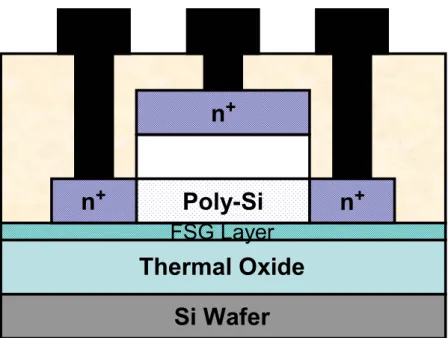
Figure 2-1 schematically depicts the process flow of the proposed poly-Si TFT. First, 500-nm-thick thermal oxide was grown on the Si wafers by furnace system to substitute for the glass substrate and all the experimental devices in this study were fabricated on thermally-oxidized Si wafers. Then, a 40-nm-thick FSG buffer layer was deposited using a PECVD system at 350°C with SiH4, CF4 and N2O as process gases.
In order to determine the effect of fluorine content in FSG layers, varying CF4 flow
rates of 10, 20, and 40 sccm, with a SiH4 flow rate of 90 sccm and a N2O rate of 5
sccm, were used to grow various FSG buffer layers, denoted by FSG1, FSG2 and FSG3, respectively. Table 2-1 lists the conditions of precursors to grow FSG buffer layers. The fluorine contents in FSG1, FSG2 and FSG3 were calculated from the SIMS profiles of the as-deposited FSG layers (as shown in Fig. 2-2) and were about 2%, 4%, and 7%, respectively.
Then, 100-nm-thick amorphous silicon layers were deposited on the FSG buffer layers in a low-pressure chemical vapor deposition (LPCVD) system with silane (SiH4)
gas source at 550°C. The deposition pressure was 100mTorr and the SiH4 flow rate
was 40sccm. Next, a semi-Gaussian-shaped KrF excimer laser with wavelength of 248nm was performed for the phase transformation from amorphous to polycrystalline silicon at the laser energy density of 420mJ/cm2 with substrate heating of 400°C under the chamber pressure of 10-3Torr. The average grain size of the poly-Si is approximately 300nm.
Individual active regions were then patterned and defined. After a clean process, a 100-nm-thick TEOS oxide was deposited with TEOS and O2 gas source by PECVD
at 350°C for gate insulator. A 200-nm-thick poly-Si was deposited to serve as the gate electrode by LPCVD. Then, gate electrode was patterned and the regions of source, drain, and gate were doped by a self-aligned phosphorous ion implantation at the dosage and energy of 5×10¹⁵ions/cm-2 and 40keV, respectively. The dopant activation was performed by excimer laser annealing with laser energy density of 220mJ/cm2, followed by a deposition of 400nm-thick passivation oxide in a PECVD system at 350°C and the definition of contact holes. Finally, a 500-nm-thick Al electrode was deposited by thermal evaporation and patterned for metal pads. For comparison, the control samples were fabricated on a 40-nm-thick conventional PECVD-oxide buffer
layer.
2.3
Method of Device Parameter Extraction
In this thesis, we use Ellipsometer to measure the thickness of poly-Si, amorphous-Si and TEOS oxide films in the fabrication procedure. All the electrical characteristics of proposed poly-Si TFTs were measured by HP 4156B-Precision Semiconductor Parameter Analyzer.
Many methods have been proposed to extract the characteristic parameters of poly-Si TFTs. In this section, those methods are described.
2.3.1 Determination of Threshold Voltage
Threshold voltage (Vth) is an important parameter required for the channel
length-width and series resistance measurements. However, Vth is not uniquely
defined. Various definitions have been proposed and the reason can be found in ID-VGS curves. One of the most common techniques is the linear extrapolation method
with the drain current measured as a function of gate voltage at a low drain voltage of 50~100mV to ensure operation in the linear region [17]. The drain current is not zero when VGS below threshold voltage and approaches zero asymptotically. Hence the IDS
versus VGS curve can be extrapolated to ID=0, and the Vth is determined from the
extrapolated intercept of gate voltage (VGSi) by
2 DS GSi th V V V = − --- (Eq. 2.1)
Equation (2.1) is strictly only valid for negligible series resistance. Fortunately series resistance is usually negligible at the low drain current when threshold voltage measurements are made. The IDS-VGS curve deviates from a straight line at gate
and mobility degradation effects. It is common practice to find the point of maximum slope of the IDS-VGS curve and fit a straight line to extrapolate to ID=0 by means of
finding the point of maximum of transconductance (Gm).
In this thesis, we use a simpler method to determinate the Vth called constant
drain current method. The voltage at a specified threshold drain current is taken as the Vth. This method is adopted in the most studied papers of poly-Si TFTs. It can be
given a threshold voltage close to that obtained by the complex linear extrapolation method. Typically, the threshold current is specified at (W/L)×10nA for VDS=0.1V and
(W/L)×100nA for VDS=5V, where W and L are channel width and channel length,
respectively.
2.3.2 Determination of Subthreshold-Swing
Subthreshold swing (S.S.) is a typical parameter to describe the control ability of gate toward channel, which reflects the turn on/off speed of a device. It is defined as the amount of gate voltage required to increase/decrease drain current by one order of magnitude.
The S.S. should be independent of drain voltage and gate voltage. However, in reality, the S.S. increases with drain voltage due to channel shortening effect such as charge sharing, avalanche multiplication and punchthrough effect. The subthreshold swing is also related to gate voltage due to undesirable and inevitable factors such as the serial resistance and interface states.
In this thesis, the S.S. is defined as one-third of the gate voltage required to decrease the threshold current by three orders of magnitude. The threshold current is specified to be the drain current when the gate voltage is equal to threshold voltage.
2.3.3 Determination of Field Effect Mobility
Usually, field effect mobility (µeff) is determined from the maximum value of
transconductance (Gm) at low drain bias. The transfer characteristics of poly-Si TFTs are similar to those of conventional MOSFETs, so that the first order of I-V relation in the bulk Si MOSFETs can be applied to poly-Si TFTs. The drain current in linear region (VDS<VGS-Vth) can be approximated as the following equation:
(
)
⎥⎦⎤ ⎢⎣ ⎡ − − ⎟ ⎠ ⎞ ⎜ ⎝ ⎛ = 2 2 1 DS DS th GS ox eff DS V V V V L W C I µ --- (Eq. 2.2)where W and L are channel width and channel length, respectively. Cox is the gate
oxide capacitance per unit area and Vth is the threshold voltage. Thus, the
transconductance is given by DS ox eff GS DS m V L W C V I g ⎟ ⎠ ⎞ ⎜ ⎝ ⎛ = ∂ ∂ = µ --- (Eq. 2.3) Therefore, the field-effect mobility is
(max) →0 = DS V m DS ox eff g WV C L µ --- (Eq.2.4)
2.3.4 Determination of ON/OFF Current Ratio
On/off current ratio is one of the most important parameters of poly-Si TFTs since a high-performance device exhibits not only a large on-current but also a small off-current (leakage current). The leakage current mechanism in poly-Si TFTs is not like that in MOSFET. In MOSFET, the channel is composed of single crystalline Si and the leakage current is due to the tunneling of minority carrier from drain region to accumulation layer located in channel region. However, in poly-Si TFTs, the channel is composed of poly-Si. A large amount of trap state densities in grain structure attribute a lot of defect states in energy band gap to enhance the tunneling effect. Therefore, the leakage current is much larger in poly-Si TFTs than in MOSFET. When
the voltage drops between gate voltage and drain voltage increases, the band gap width decreases and the tunneling effect becomes much more severe. Normally we can find this effect in typical poly-Si TFTs’ IDS-VGS characteristics where the
magnitude of leakage current will reach a minimum and then increase as the gate voltage decreases/increases for n/p-channel TFTs.
There are a lot of ways to specify the on and off-current. In this chapter, take n-channel poly-Si TFTs for examples, the on-current is defined as the drain current when gate voltage at the maximum value and drain voltage is 5V. The off-current is specified as the minimum current when drain voltage equals to 5V.
V V at Plot V I of Current Minimum V V at Plot V I of Current Maximum I I DS GS DS DS GS DS OFF ON 5 5 = − = − = --- (Eq. 2.5)
2.3.5 Extraction of Grain Boundary Trap State Density
The Trap State Density (Nt), which can be determined by the theory established
by Levinson et al. [18], which is based on Seto’s theory [19].
For poly-Si TFTs, the drain current IDS can be given as following:
⎟ ⎟ ⎠ ⎞ ⎜ ⎜ ⎝ ⎛ − ⎟ ⎠ ⎞ ⎜ ⎝ ⎛ = GS ox Si c t GS DS ox FE DS V kTC L N q V V L W C I ε µ 8 exp 2 3 --- (Eq. 2.6) Where,
µeff field-effect mobility of carriers
q electron charge
k Boltzmann’s constant
εSi dielectric constant of silicon
T temperature
Nt trap-state density per unit area
Lc channel thickness
This expression, first developed by Levinson et al., is a standard MOSFET’s equation with an activated mobility, which depends on the grain-boundary barrier
height. Levinson et al. assumed that the channel thickness was constant and equal to the thickness of the poly-Si film (t). This simplifying assumption is permissible only for very thin film (t<10nm). The trap-state density can be obtained by extracting a straight line on the plot of ln(IDS/VGS) versus 1/VGS at low drain voltage and high gate
voltage.
Proano et al. [20] thought that a barrier approximation is to calculate the gate induced carrier channel thickness by solving Poisson’s equation for an undoped material and to define the channel thickness (Lc) as a thickness in which 80% of the
total charges were induced by the gate. Doing so, one obtains
(
)
fb GS SiO Si ox c V V q kTt L − = 2 8 ε ε --- (Eq. 2.7) which varies inversely with (VGS−Vfb). This predicts, by substituting Eq.2.7 intoEq.2.6, that ln[IDS/(VGS−Vfb)] versus 1/(VGS−Vfb)2. We use the gate voltage at which
minimum leakage current occurs as flat-band voltage (Vfb). Effective trap-state
density (Nt) can be determined from the square root of the slope.
2.4
Results and Discussion
2.4.1 Characteristics of Poly-Si TFTs on FSG layer
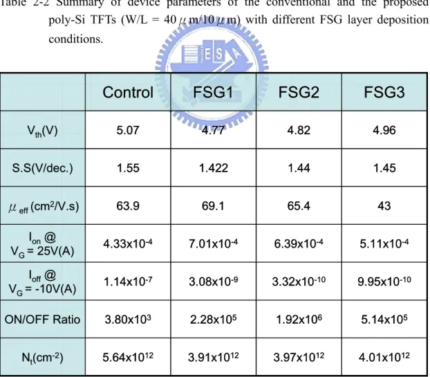
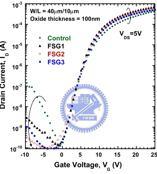
Figure 2-3 shows the transfer characteristics (IDS-VGS) of the conventional and
the proposed poly-Si TFTs with different FSG buffer layers. The measurements was performed at drain voltage of VDS=5V. The measured and extracted parameters from
the devices are listed in Table 2-2. The threshold voltage, subthreshold swing, on-current (VGS=25V), and off-current (VGS=-10V) were measured at VDS=5V.
layers exhibit better on-state and off-state characteristics than those of the control sample. Notably, under a large negative gate bias, the leakage currents of the TFTs on FSG layers (3.08×10⁻⁹A, 3.32×10⁻¹⁰A, and 9.95×10⁻¹⁰A for FSG1, FSG2, and FSG3, respectively) are over one order of magnitude lower than that on the conventional oxide buffer layer (1.14×10⁻⁷A). This is attributed to the facts that the reduced the traps by the incorporation of fluorine in the poly-Si films during ELA [13] and the released tensile stress at the poly-Si/buffer-oxide-layer interface [16]. Moreover, the threshold voltage and subthreshold swing of the poly-Si TFTs on FSG layers (4.77V & 1.422V/dec., 4.82V & 1.44V/dec., and 4.95V & 1.45V/dec. for FSG1, FSG2, and FSG3, respectively) were found to be superior to those of the control sample (5.07V & 1.55V/dec.).
It has been revealed that the threshold voltage and subthreshold swing are more sensitive to the density of deep trap states near midgap associated with the dangling bonds [4]. For this reason, it is inferred that the dangling bonds within the poly-Si channel and SiO2/poly-Si interface were effectively passivated by fluorine atoms.
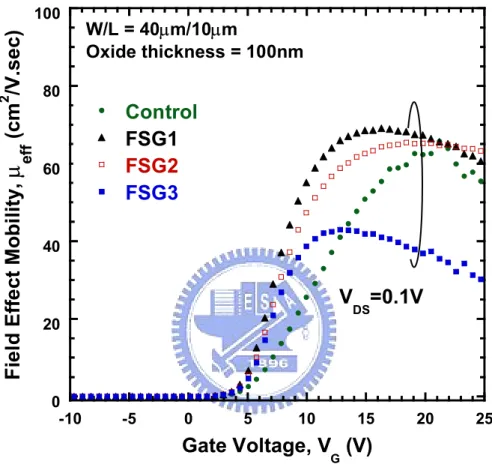
Figure 2-4 shows the field-effect mobility of the conventional and the proposed poly-Si TFTs. They were found to be 63.9cm2/V.s, 69.1cm2/V.s, 65.4cm2/V.s, and 43cm2/V.s for control, FSG1, FSG2, and FSG3, respectively. As can be seen, except FSG3, the field-effect mobility was improved by the incorporation of fluorine atoms within the poly-Si channel. It was demonstrated that the field-effect mobility is significantly influenced by the tail states near the band edge caused by the strain bonds in poly-Si and SiO2/Si interface [4]. Therefore, we believe that fluorine atoms
introduced into poly-Si channel can not only passivate the dangling bonds, but also release the strain bonds within the poly-Si channel and SiO2/poly-Si interface.
However, for the degradation phenomenon in FSG3, we will explain later.
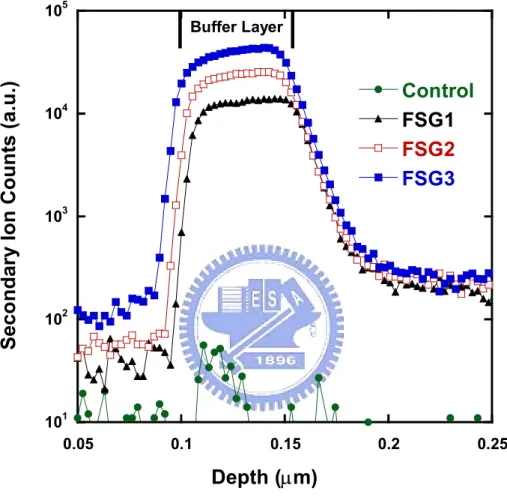
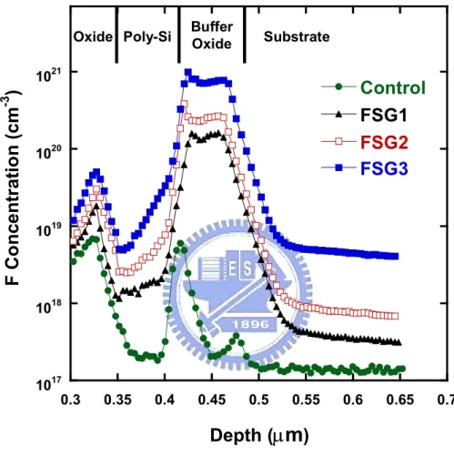
SIMS profiles of fluorine, as shown in Fig. 2-5. It was clearly observed that considerable fluorine atoms were introduced and confined in the poly-Si for the FSG samples and, in particular, two fluorine peaks were located at the top and bottom interfaces. Therefore, we believe that the grain boundary trap states, both the top and bottom interface states were terminated by fluorine atoms. Moreover, in order to verify the effect of fluorine passivation, the effective trap state density (Nt) was
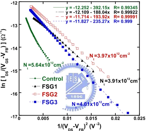
calculated. Figure 2-6 shows the plot of ln(IDS/VGS) versus 1/VGS at low drain voltage
and high gate voltage for all samples. The effective trap state density caculated form the slopes for the control, FSG1, FSG2, FSG3 were 5.64×1012cm-2, 3.91×1012cm-2, 3.97×1012cm-2, and 4.01×1012cm-2, respectively. These figures strongly hint that the fluorine can effectively passivate the present trap states in poly-Si channel region.
However, the FSG3 shows a detrimental effect on the performance of the resulting TFT. This is attributed to the moisture absorption. According to previous report, the moisture absorption increased with increasing fluorine content in the FSG layers [21]. The absorbed moisture would easily form OH or react with fluorine to form HF, which in turn deteriorate the devices and result in the degraded performance and reliability [22].
2.4.2 Uniformity and Reliability of Poly-Si TFTs on FSG layer
Figure 2-7 displays the statistical distributions of the field-effect mobility (µeff),
the leakage current (Ioff), and the threshold voltage (Vth) of the conventional and the
proposed poly-Si TFTs with different FSG buffer layer deposition conditions. The vertical bars in the figure indicate the minimum and maximum values of the devices characteristics and the squares present the average values. The average values of the µeff for the control, FSG1, FSG2 and FSG3 samples were 57.7cm2/V.s, 66.7cm2/V.s,
63.9cm2/V.s, and 45.2cm2/V.s with standard deviations of 4.05, 2.98, 3.09 and 4.15, respectively. This tendency indicates that with moderate fluorine content in FSG layers the average values and the deviations of µeff can be greatly improved. Also, the
average values of the Ioff for the control, FSG1, FSG2, and FSG3 samples were
6.8×10⁻⁸A, 7.8×10⁻⁹A, 1.3×10⁻⁹A, and 1.8×10⁻⁹A with standard deviations of
8.14×10⁻⁸, 2.46× 10⁻⁹, 6.55×10⁻¹⁰ and 1.93×10⁻⁹, respectively. The average of the V th
for the control, FSG1, FSG2, and FSG3 samples were 5.50V, 5.2V, 4.89V, and 4.88V with standard deviations of 0.21, 0.037, 0.22 and 0.13, respectively. These results imply that fabricating poly-Si TFTs on FSG buffer layers with moderate fluorine concentration can improve the device performance as well as the uniformity of its characteristics. The uniformity of the poly-Si TFTs is strongly affected by the random distribution of grain boundaries. Therefore, using fluorine to terminate those trap states within poly-Si channel can effectively alleviate the influence of grain boundaries.
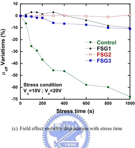
Then, we would discuss the reliability issue of the conventional and the proposed poly-Si TFTs with different FSG buffer layer deposition conditions. The hot-carrier stress was performed at VD,stress=20V, VG,stress=10V, and source electrode
grounded for 1000sec to investigate the device reliability. Figure 2-8 plots the variations of on-state current (Ion), threshold voltage (Vth), and field-effect mobility
(µeff) over stress time. The variations of Ion, Vth,and µeff were defined as (Ion,stressed-
Ion,initial)/Ion,initial×100%, (Vth,stressed-Vth,initial)/Vth,initial×100%, and (µeff,stressed-µeff,initial)
/µeff,initial×100%, respectively, where Ion,stressed, Vth,stressed, µeff,stressed, Ion,initial, Vth,initial, and
µeff,initial represent the measured values before and after electrical stress.
Notably, the control shows relatively large variations in Ion, Vth, and µeff after
1000sec stress, whereas the FSG2 has slight change in Ion and Vth and stays almost
greatly reduced the device degradation under hot carrier stress, which is due to the formation of the rather strong Si-F bonds. Since the calculated percentages of fluorine content in the FSG layers are 2%, 4% and 7% for FSG1, FSG2, and FSG3, respectively, we deduce based on the above experimental results that the trap states can be effectively passivated when the fluorine content in the FSG is above 2%; while the absorbed moisture in the FSG as the content of fluorine is above 4% starts to induce visible corrosion of the poly-Si structures after competing with the trap states termination. Definitely, the corrosion becomes more severe as the content of fluorine reached 7%. As a result, the optimized condition of fluorine content of FSG is probably within 2% to 4%.
2.5
Summary
A process-compatible scheme for fabricating poly-Si TFTs on an FSG buffer layer is proposed. Significant improvements in the device performance and uniformity were successfully demonstrated with fluorine incorporation in the poly-Si layer. This is attributed to the reduction of the trap state density in poly-Si and SiO2 interface.
Additionally, the incorporation of fluorine atoms also promotes the hot-carrier immunity due to the formation of the strong Si-F bonds. Fabricating poly-Si TFTs on FSG buffer layers with appropriate fluorine content improves not only the electrical performance and uniformity but also the reliability.
References:
[1] T. Serikawa, S. Shirai, A. Okamoto, and S. Suyama, “Low-temperature fabrication of high-mobility poly-Si TFT’s for large-area LCD’s,” IEEE Trans. Electron
Devices, vol. 36, pp. 1929-1933, Sept. 1989.
[2] G. K. Guist and T. W. Sigmon, “High-performance thin-film transistors fabricated using excimer laser processing and grain engineering,” IEEE Trans. Electron
Devices, vol. 45, pp. 925-932, Apr. 1998.
[3] N. Kudo, N. Kusumoto, T. Inushima, and S. Yamazaki, “Characterization of polycrystalline-Si thin-film transistors fabricated by excimer laser annealing method,” IEEE Trans. Electron Devices, vol. 40, pp. 1876-1879, Oct. 1994.
[4] I. W. Wu, W. B. Jackson, T. Y. Huang, A. G. Lewis, and A. Chiang, “Passivation kinetics of two types of defects in polysilicon TFT by plasma hydrogenation,”
IEEE Electron Device lett., vol. 12, pp. 181-183, May 1991.
[5] I-Wei Wu, Warren. B. Jackson, Tiao-Yuan Huang, Alan G. Lewis, and Anne Chiang, “Mechanism of device degradation in n- and p-channel polysilicon TFT’s by electrical stressing,” IEEE Electron Device lett., vol. 11, pp. 167-170, 1990. [6] E. Fujii, K. Senda, F. Emoto, A. Yamamoto, A. Nakamura, Y. Uemoto, and G.
Kano, “A leaser-recrystallization technique for silicon-TFT integrated circuits on quartz substrates and its application to small-size monolithic active-matrix LCD’s,” IEEE Trans. Electron Devices, vol. 37, pp. 121-127, Jan. 1990.
[7] M. Cao, S. Talwar, K. J. Kramer, T. W. Sigmon, and K. C. Saraswat, “ A high-performance polysilicon thin-film transistor using XeCl excimer laser crystallization of pre-patterned amorphous Si films,” IEEE Trans. Electron
Devices, vol. 43, pp. 561-567, Apr. 1996.
crystalline phase and stress in laser-crystallized poly-Si thin films by Raman spectroscopy,” Jpn. J. Appl. Phys., vol. 38, pp. L1312-1314, 1999.
[9] S. Higashi, N. Ando, K. Kamisako, and T. Sameshima, “Stress in pulsed-laser-crystallized silicon films,” Jpn. J. Appl. Phys., vol. 40, pp. 731-735, 2001.
[10] H. N. Chern, C. L. Lee, and T. F. Lei, “The effects of fluorine passivation on polysilicon thin film transistors,” IEEE Trans. Electron Devices, vol. 41, pp. 698-702, May 1994.
[11] S. Maegawa, T. Ipposhi, S. Maeda, H. Nishimura, T. Ichiki, M. Ashida, O. Tanina, Y. Inoue, T. Nishimura and N. Tsubouchi, “Performance and reliability improvement in poly-Si TFT’s by fluorine implantation into gate poly-Si,” IEEE
Trans. Electron Devices, vol. 42, pp. 1106-1112, Jun. 1995.
[12] J. W. Park, B. T. Ahn and K.Lee, “Effects of F+ implantation on the characteristics of poly-Si films and low-temperature n-ch poly-Si thin-film transistors,” Jpn. J. Appl. Phys., vol. 34, pp. 1436-1441, Mar. 1995.
[13] C. H. Kim, S. H. Jung, J. S. Yoo, and M. K. Han, “Poly-Si TFT fabricated by laser-induced in-situ fluorine passivation and laser doping,” IEEE Electron Device
lett., vol. 22, pp. 396-398, Aug. 2001.
[14] C. L. Fan, and M. C. Chen, “Performance improvement of excimer laser annealed poly-Si TFTs using fluorine ion implantation,” Electrochemical and
Solid State Lett., 5 (8), G75-G77, 2002.
[15] C. H. Kim, S. H. Jung, J. S. Yoo, and M. K. Han, “Poly-Si TFT fabricated by laser-induced in-situ fluorine passivation and laser doping,” IEEE Electron Device
lett., vol. 22, pp. 396-398, Jun. 2001.
[16] Y. Mitani, H. Satake, Y. Nakasaki, and A. Toriumi, “Improvement of charge-to-breakdown distribution by fluorine incorporation into thin gate oxides,”
IEEE Trans. Electron Devices, vol. 50, pp. 2221-2226, Nov. 2003.
[17] Dieter K. Schroder, “Semiconductor Material and Device Characterization,”
Wiley-INTERSCIENCE, 1998
[18] J. Levinson, G. Este, M. Rider, P. J. Scanlon, F. R. Shepherd, and W. D. Westwood, “Conductivity behavior in polycrystalline semiconductor thin film transistors,” J. Appl. Phys., vol. 53, no. 2, pp. 193, 1982
[19] J. Y. W. Seto, “The electrical properties of polycrystalline silicon films,” J. Appl.
Phys., vol. 46, no. 12, pp. 5247, 1975
[20] R. E. Proano, R. S. Misage, D. Jones, and D. G. Ast, “Development and electrical properties of undoped polycrystalline silicon thin film transistors,” IEEE Trans.
Electron Devices, vol. 36, no. 9, pp. 1915, 1989.
[21] H. Miyajima, R. Katsumata, Y. Nakasaki, Y. Nishiyama, and N. Hayasaka, “Water absorption properties of fluorine-doped SiO2 films using plasma-enhanced
chemical vapor deposition,” Jpn. J. Appl. Phys., vol. 35, pp. 6217-6225, 1996. [22] G. Passemard, P. Fugier, P. Nobl, F. Pries, and O. Demolliens, “Study of fluorine
stability in fluoro-silicate glass and effects on dielectric properties,”
Thermal Oxide
Si Wafer
(a) Thermal oxidation grown by furnace.
Thermal Oxide
Si Wafer
FSG Layer
(b) FSG layer deposited by PECVD.
Thermal Oxide
Si Wafer
FSG Layer
a-Si
Thermal Oxide
Si Wafer
FSG Layer
Poly-Si Channel
(d) Recrystallization of a-Si film into poly-Si channel by ELA, active region defined.
Thermal Oxide
Si Wafer
FSG Layer
Poly-Si Channel
TEOS Gate Oxide
Poly-Si Gate
Thermal Oxide
Si Wafer
FSG Layer
Poly-Si Channel
Phosphorous self-aligned ion implantation
(f) The gate electrode defined and self-align phosphorous ion implantation.
Thermal Oxide
Si Wafer
FSG Layer
Poly-Si
n
+n
+n
+Thermal Oxide
Si Wafer
FSG Layer
Poly-Si
n
+n
+n
+(h) Deposition of passivation oxide, contact holes opened and metal pads formation.
Table 2-1 Summary of different deposition conditions of FSG buffer layer.
5
90
40
FSG3
5
90
20
FSG2
5
90
10
FSG1
5
90
0
Control
SiH
4N
2O
CF
4 Gas Sample Unit:
sccm5
90
40
FSG3
5
90
20
FSG2
5
90
10
FSG1
5
90
0
Control
SiH
4N
2O
CF
4 Gas Sample5
90
40
FSG3
5
90
20
FSG2
5
90
10
FSG1
5
90
0
Control
SiH
4N
2O
CF
4 Gas Sample Unit:
sccmTable 2-2 Summary of device parameters of the conventional and the proposed poly-Si TFTs (W/L = 40μm/10μm) with different FSG layer deposition conditions. 4.01x10¹² 3.97x10¹² 3.91x10¹² 5.64x10¹² Nt(cm-2) 5.14x10⁵ 1.92x10⁶ 2.28x10⁵ 3.80x10³ ON/OFF Ratio 9.95x10⁻¹⁰ 3.32x10⁻¹⁰ 3.08x10⁻⁹ 1.14x10⁻⁷ Ioff@ VG = -10V(A) 5.11x10⁻⁴ 6.39x10⁻⁴ 7.01x10⁻⁴ 4.33x10⁻⁴ Ion@ VG = 25V(A) 43 65.4 69.1 63.9 μeff(cm2/V.s) 1.45 1.44 1.422 1.55 S.S(V/dec.) 4.96 4.82 4.77 5.07 Vth(V)
FSG3
FSG2
FSG1
Control
4.01x10¹² 3.97x10¹² 3.91x10¹² 5.64x10¹² Nt(cm-2) 5.14x10⁵ 1.92x10⁶ 2.28x10⁵ 3.80x10³ ON/OFF Ratio 9.95x10⁻¹⁰ 3.32x10⁻¹⁰ 3.08x10⁻⁹ 1.14x10⁻⁷ Ioff@ VG = -10V(A) 5.11x10⁻⁴ 6.39x10⁻⁴ 7.01x10⁻⁴ 4.33x10⁻⁴ Ion@ VG = 25V(A) 43 65.4 69.1 63.9 μeff(cm2/V.s) 1.45 1.44 1.422 1.55 S.S(V/dec.) 4.96 4.82 4.77 5.07 Vth(V)FSG3
FSG2
FSG1
Control
101 102 103 104 105 0.05 0.1 0.15 0.2 0.25
Control
FSG1
FSG2
FSG3
Se
co
nda
ry
Ion
Cou
n
ts
(a
.u.)
Depth (
µm)
Buffer LayerFig. 2-2 SIMS profiles of the FSG layer as-deposited samples with different FSG layer deposition conditions.
10-10 10-9 10-8 10-7 10-6 10-5 10-4 10-3 -10 -5 0 5 10 15 20 25
FSG3
Control
FSG1
FSG2
Dr
a
in Curr
en
t,
I
D(A
)
Gate Voltage, V
G(V)
V
DS=5V
W/L = 40µm/10µm Oxide thickness = 100nmFig. 2-3 Transfer characteristics of the conventional and the proposed poly-Si TFTs with different FSG layer deposition conditions.
0 20 40 60 80 100 -10 -5 0 5 10 15 20 25
Control
FSG1
FSG2
FSG3
Fi
el
d Eff
e
ct Mo
bi
lity
,
µ
eff(cm
2/V.se
c
)
Gate Voltage, V
G(V)
W/L = 40µm/10µm Oxide thickness = 100nmV
DS=0.1V
Fig. 2-4 Field effect mobility of the conventional and the proposed poly-Si TFTs with different FSG layer deposition conditions.
1017 1018 1019 1020 1021 0.3 0.35 0.4 0.45 0.5 0.55 0.6 0.65 0.7
Control
FSG1
FSG2
FSG3
F Co
nc
e
n
tratio
n (cm
-3)
Depth (
µm
)
Oxide Poly-Si BufferOxide Substrate
Fig. 2-5 SIMS profiles of the conventional and the proposed poly-Si TFTs with different FSG layer deposition conditions.
-17 -16 -15 -14 -13 -12 0 0.005 0.01 0.015 0.02 0.025
Control
FSG1
FSG2
FSG3
y = -12.252 - 392.15x R= 0.99345 y = -12.109 - 188.04x R= 0.99922 y = -11.714 - 193.92x R= 0.99991 y = -11.827 - 235.27x R= 0.999ln
[
I
DS/(
V
GS-V
FB) ]
(Ω
-1)
1/(V
DS-V
FB)
2(V
-2)
N t=5.64x10 12 cm-2 N t=3.91x10 12 cm-2 N t=3.97x10 12 cm-2 N t=4.01x10 12 cm-2Fig. 2-6 Trap state density extraction of the conventional and the proposed poly-Si TFTs with different FSG layer deposition conditions.
Buffered FSG Oxide
control FSG1 FSG2 FSG3
Field Effect Mobility (cm
2
/V.s)
30 40 50 60 70 80 VDS=0.1V W/L=40um/10um Buffered FSG Oxide control FSG1 FSG2 FSG3Field Effect Mobility (cm
2
/V.s)
30 40 50 60 70 80 VDS=0.1V W/L=40um/10um(a) Field effect mobility distribution
Buffered FSG Oxide
control FSG1 FSG2 FSG3
L
eakage Current (A)
10-12 10-11 10-10 10-9 10-8 10-7 10-6 10-5
`
Buffered FSG Oxide
control FSG1 FSG2 FSG3Threshold Voltage (V)
4.0 4.5 5.0 5.5 6.0 6.5 7.0(c) Threshold voltage distribution
Fig. 2-7 Distribution of (a) filed-effect mobility and (b) leakage current of the poly-Si TFTs on different buffer layers. The vertical bars indicate the minimum and maximum values of the devices characteristics and the squares are the average values.