國
立
交
通
大
學
光電工程研究所
碩
士
論
文
調變光子晶體平板方向耦合器的非耦合點研究
Tuning the Decoupling Point of the Directional Coupler
in a Photonic Crystal Slab
研 究 生:李柏毅
指導教授:謝文峰 教授
調變光子晶體平板方向耦合器的非耦合點研究
Tuning the Decoupling Point of the Directional Coupler
in a Photonic Crystal Slab
研 究 生:李柏毅 Student:Po-Yi Lee
指導教授:謝文峰 教授 Advisor:Prof. Wen-Feng Hsieh
國 立 交 通 大 學
光電工程研究所
碩 士 論 文
A Thesis
Submitted to Institute of Electro-Optical Engineering College of Electrical Engineering and Computer Science
National Chiao Tung University in partial Fulfillment of the Requirements
for the Degree of Master
in
Electro-Optical Engineering June 2010
Hsinchu, Taiwan, Republic of China
調變光子晶體平板方向耦合器的
非耦合點研究
研究生:李柏毅 指導老師:謝文峰 教授
國立交通大學光電工程研究所
摘要
以三角晶格排列的光子晶體製成耦合器,其兩條色散曲線會相交於非
耦合點(decoupling point),當光以非耦合點的頻率入射其中一條波導時,
入射光波只會在入射的波導中傳播,並不會耦合至另一條波導。藉由廣義
的緊束縛理論對兩條缺陷波導間的耦合效應加以分析,我們發現當橫向調
變耦合器的兩條線缺陷間距時,由於耦合係數產生改變,非耦合點的本徵
頻率會有藍移的現象,因此改變了方向耦合器的非耦合點頻率及耦合長
度。另一方面,沿著波傳播方向縱向移動兩條波導,能使正方晶格的方向
耦合器產生非耦合點。
在此論文中我們也運用數值方法,對兩種不同型態:介電柱與空氣洞
所構成的方向耦合器的色散關係加以模擬;並且成功的運用緊束縛理論,
解釋上述將缺陷調變所引起的現象。再藉由模擬所得到的結果,提出對光
Tuning the Decoupling Point of the Directional Coupler
in a Photonic Crystal Slab
Student: Po-Yi Lee Advisor: Prof. Wen-Feng Hsieh
Institute of Electro-Optical Engineering
National Chiao Tung University
Abstract
Two dispersion curves of the photonic crystal (PC) coupler with triangular lattices will cross at the so-called decoupling point. When a light wave is launched into one of the waveguide at the frequency of this point, it will propagate only in the incident waveguide without coupling into the other one. Using the extended tight-binding theory (TBT) to analyze the coupling effects between two defect waveguides, we found that the eigenfrequency of the decoupling point blue shifts as adjusting the separation of two line defects transversely of the coupler. The magnitude of coupling coefficients wound also change to affect the decoupling frequency and the coupling length of the directional coupler (DC). Longitudinal shifting two waveguides along the wave propagation direction can also shift the dispersion of the square lattice DC so that the decoupling point would exist in the square lattice DC. In this thesis, we use numerical methods to simulate dispersion relations of two different types of DCs: dielectric rod and the air-hole types. Moreover, we successfully use the TBT to explain these phenomena and give a designing rule based on the TBT for tuning the decoupling frequency of the PC coupler.
致謝
剛進實驗室時的迎新還歷歷在目,現在卻已經在寫論文的致謝了。在這兩年的學校 生活,環境促使我不斷的學習與成長,完成了碩士論文,通過了畢業口試,除此之外, 更認識了很多的朋友,充滿了許許多多回憶,也感謝大家一直以來的協助,無論是學業 上,或是生活上。 最感謝的,當然是謝文峰老師,謝謝老師這兩年來的指導,初入實驗室學識尚淺時, 老師總是耐心的帶領導讀,教我們如何去看一篇 paper;在研討時,適時引導我們解開 疑惑;到了最後畢業前,不厭其煩逐字逐句幫我們修改論文上的瑕疵,這麼 nice 的老 師,很難找到了。除了學業上,也很感謝老師時常會關心我們生活上的情況。 再來要謝謝至賢學長,對於我在光子晶體領域的指導,常常要麻煩你幫忙修改文 章,解答我天馬行空的問題;小豪學長,謝謝你當我五月初入實驗室,人生地不熟時, 帶領我去認識實驗室的各位學長以及研究領域,以及幫我們拍超專業的畢業照;謝謝松 哥幫忙處理 cluster 上的問題,還讓我去學高溫爐以及 ALD;謝謝黃董在實驗室出遊少 車時,二話不說就答應幫忙;謝謝智彰學長常分享一些知道的資訊給我;謝謝小郭學長 在 meeting 時常以不同領域的觀點提出看法,讓我能做不少修正;謝謝 Bogi 學長常常 一起去棒球場傳接球;謝謝信民學長,當我第一次去工研院時請我吃飯,還印了一本論 文讓我學習;謝謝智雅學姊考古題的強大奧援,以及厚仁學長幫我們拍畢業照,以上兩 位我會非常期待收到你們的喜帖~。還有感謝吳博見面時常主動關心我;常請我喝飲 料,拉我去聊天的維仁學長。 另外感謝有義氣的建輝常帶我去吃好吃的,和我聊物理、電影、文學、科技、說垃 圾話,無所不聊,陪我一起嘴砲,一起吐槽;帶我進入健身的領域的冠智,我們總是一 邊鍛鍊肌肉,一邊談八卦、聊心事~,恭喜你出國留學的目標先實現了;八卦中人的阿 肥,自從你先離開後,就沒人和我說流言啦~。 自稱不愛說垃圾話可是一點都不中肯的阿登,相信你的實驗一定會成功有結果;光子晶體組的傳人唯碩,對未來不用太擔心,按部就班就能順利畢業了;程式高手的家瑋, 謝謝你幫我處理 Linux 上的一些問題;創造出許多傳說的實驗室小精靈們:玠翰恭喜你 有新鮮健康的肝,人生是彩色的,將來可以加入國軍弟兄,但祝你還是先回 lab 繼續燃 燒;誌軒感謝你每晚為大家堅守實驗室到深夜,營造出 lab 燈火通明,似乎大家晚上也 很努力的情景。 當然還有一起度過兩年碩士生活的小布丁,真的謝謝你常在我心情不好時,聽我說 話,陪我聊天,當我的聆聽者。 在最後,感謝我的好朋友,在我徬徨時,聽我的想法,分享意見;在我情緒低潮時, 聽我吐苦水,傾訴心情。 實驗室裡的吉他,伴我消磨了無數時光,希望我離開後,能有下個知音之人。 謝謝所有的大家!讓我擁有充滿這麼多回憶的兩年。 感謝國科會計畫 NSC96-2628-M-009-001-MY3 對此研究的支持。 柏毅 于新竹交大 2010 夏
Content
Abstract (in Chinese)...i
Abstract (in English)...iii
Acknowledgements...iv
Contents...vi
List of Figures...viii
Chapter 1 Introduction...1
1-1 Photonic crystal...1
1-2 Photonic crystal waveguide...2
1-3 Directional coupler...2
1-4 Numerical methods...3
1-4-1 Plane wave expansion method...3
1-4-2 Finite-difference time-domain method...5
1-5 Motivation...9
1-6 Organization of the thesis...11
Chapter 2 Theoretical Analysis...12
2-1 Tight-binding theory (TBT)...12
2-2 TBT in the dielectric rod slab...12
Chapter 3 Simulation Results and Discussion...23
3-1 Shifting dielectric rod defects in the photonic crystal slab...23
3-1-1 Shifting a point defect...25
3-1-2 Shifting a line defect...26
3-1-3 Shifting line defects of directional couplers in triangular and square
lattices...28
3-2 Shifting air-hole defects in the photonic crystal slab...32
3-2-1 Shifting a point defect...34
3-2-2 Shifting a line defect...36
3-2-3 Shifting line defects of directional couplers...38
3-3 Coupling lengths calculated by the FDTD method...41
Chapter 4 Conclusion and Perspectives...45
4-1 Conclusion...45
4-2 Perspectives...45
List of Figures
Fig. 1.1 Field components of a three-dimensional Yee cell……….……...8
Fig. 1.2 Two types of PC slabs...……...………...…….………...9
Fig. 2.1 The geometric structure of a single PCW dielectric rod slab.………....………...13
Fig. 2.2 Ez of a point defect localized at the center of the dielectric rod PC slab...14
Fig. 2.3 Ways of shifting defect rods in the single PCW...15
Fig. 2.4 The geometric structure of a double PCWs dielectric rod slab...16
Fig. 2.5 Ways of shifting defect rods in the coupled PCWs...17
Fig. 2.6 The geometric structure of a single PCW slab made of air-hole...18
Fig. 2.7 Electric fields of a point defect localized at the center of the air-hole PC slab...19
Fig. 2.8 Ways of shifting defect holes in the single PCW...20
Fig. 2.9 The geometric structure of a double PCWs air-hole slab...20
Fig. 2.10 Ways of shifting defect holes in the coupled PCWs...22
Fig. 3.1 Dispersion relations of a perfect dielectric rod PC slab with square lattices of the TM-like and the TE-like EM waves...24
Fig. 3.2 The refractive index of silicon at different wavelength...24
Fig. 3.3 The eigenfrequency of the point defect with a defect rod located at different positions along the y-axis...25
Fig. 3.4 The electric fields of the point defect made of a dielectric rod along the y and x axes...26
Fig. 3.5 Dispersion curves of a single waveguide slab with all the defect rods are moved toward the y and x direction...27
Fig. 3.6 Dispersion relations of the DCs with defect rods are moved transversely...28 Fig. 3.7 The dispersion relation of a triangular lattice DC with defect waveguides
are shifted transversely and with a fixed separation...30
Fig. 3.8 Change of parity in a symmetric dielectric rod DC...30 Fig. 3.9 Dispersion relations of shifting double defect rod channels longitudinally in two
different lattices PC slabs...31
Fig. 3.10 The values of α, β and 2β α as defect rods shifted in x direction in a
square lattice DC...32
Fig. 3.11 Dispersion relations of a perfect triangular lattice air-hole PC slab of the TE-like
and TM-like polarizations incident EM waves...33
Fig. 3.12 Dispersion relations of a perfect air-hole PC slab with square lattices and the
TE incident EM wave...34
Fig. 3.13 The eigenfrequency of the air-hole point defect located at different positions
along the y and x axes...35
Fig. 3.14 Ex and Ey of an air-hole point defect shifted toward the y and x axes...35
Fig. 3.15 Dispersion curves of a single PCW air-hole slab with all the defect holes are
shifted toward the y and x directions...37
Fig. 3.16 Dispersion curves of the DCs with defect holes are moved transversely...38 Fig. 3.17 The values of α, β and 2β α as defect holes shifted in y direction
simultaneously...39
Fig. 3.18 The values of α, β and 2β α as defect holes shifted to approach in the
y direction...40
Fig. 3.19 The values of α, β and 2β α as defect holes shifted to apart from
each other in the y direction...40
Fig. 3.20 Dispersion curves as moving all the defect holes along the x direction in the
Fig. 3.21 The values of α, β and 2β α as defect holes shifted in x direction in the
triangular lattice DC...41
Fig. 3.22 Propagating EM waves in the dielectric rod DC...42 Fig. 3.23 The coupling lengths of different shift of waveguides in the dielectric
rod DC...42 Fig. 3.24 Propagating EM waves in the air-hole DC...43 Fig. 3.25 The coupling lengths of different shift in the air-hole DC...44
Chapter 1 Introduction
1-1
Photonic crystal
Over the recent twenties years, photonic crystals (PCs) and the related photonic bandgap devices have attracted a great deal of attentions in fabricating all optical integrated circuits. The concept of the PC was first proposed by Eli Yablonovitch [1] and Sajeev John [2] in 1987. Yablonovitch presented that a structure can offer a photonic bandgap (PBG), hence electron-hole pairs of a semiconductor cannot recombine within a range of frequencies and therefore no spontaneous emission occurs. Sajeev John also proposed photons can be localized by the PC defect, similar as the physical property of electrons. Afterward two professors used the PC and the PBG to denominate related researches of these new fields.
A PC is usually composed of periodically arranging dielectric materials with large refractive index difference. Such structure possesses a complete PBG [3]. Within the PBG of the PC, a certain range of frequencies of electromagnetic (EM) waves is disallowing to propagate and therefore suppress a band of frequencies from existing. Because there are no corresponding propagation modes in the bandgap, the incident EM wave is completely reflected. We can well design and construct PCs with PBGs to prevent light from propagating in certain directions with specified frequencies.
There are no extended states in the PBG of a perfect PC. As we introduce a defect to break the translational symmetry, the defect may permit localized modes to exist with frequencies within the bandgap. Introducing defects to PCs means to have the lattice points or locations dissimilar from the perfect arranged structure. Defects can change the band structure of a perfect PC and allow guided modes to exist inside the bandgap. For a point defect, a mode can be localized whenever its frequency is in the PBG. By using line defects,
one can guide light from one location to another. We can alter the mechanisms of PCs by introducing various defects. The characteristic of the PBG provides many novel applications, such as using a PC block to form photonic reflector [4], introducing line defects in the PC to construct a waveguide, or creating a point defect (or several defects) to form a PC resonant cavity [5].
1-2
Photonic crystal waveguide
The photonic crystal waveguide (PCW) can be created by modifying a linear sequence of unit cells. As we introducing a line defect into a perfect PC, a defect-guided mode is formed within the bandgap. A light wave will be restricted to transmit in this channel. In traditional total internal reflection waveguides, light is only restricted to propagate in high refractive index materials. Besides, the bending angle for changing the light propagation direction of traditional waveguides cannot exceed 1 degree, otherwise the energy loss is significant; this disadvantage make the scale of optical devices increases. Conversely, PCWs allow light to propagate in a low refractive index medium, like air. Light that propagates in the PCW with a frequency within the bandgap of the PC is confined to the defects and can directly transfer along the defects. Consequently, PCWs provide low energy loss and high light confinement even through a sharply bend [6]. The PCWs are the most promising elements of PCs for designing photonic integrated circuits.
1-3
Directional coupler
A directional coupler (DC) which can be used in light switches [7,8], beam splitters [9,10], and modulators [11] is formed by arranging a pair of parallel PCWs separated by one or several rows of partition rods or holes. A symmetric DC possesses two dispersion curves with an even mode and an odd mode, respectively. As two waveguides are quite close, their fields will overlap. An EM wave with a given frequency is incident into one PCW of the
coupler will transfer entirely to the other waveguide as transmitted a certain distance, which is called the coupling length. The coupling length is defined as π Δk, where Δk is the wavevector mismatch of the two dispersion curves at the operation frequency. As designing the wavelength-selective devices such as the demultiplexer [12], the coupling length of a DC is considerable. The transmission efficiency of the PC coupler can be improved by properly tuning the formation of defects. Different claddings of the coupler also vary vertical confinements of light, which propagates in the PCWs of the DC. With various applications, DCs are also major devices for the optical communication.
1-4
Numerical methods
To investigate the propagation of EM waves through a PC structure, there are several efficient and accurate algorithms such as plane wave expansion method (PWEM) [13] and finite-difference time-domain (FDTD) method [14]. The PWEM is well at calculating the bandgap for a specific polarization, dispersive properties, and eigenmodes of infinite periodic structures. The FDTD method is widely used to estimate transmission and reflection spectra for computational EM problems.
1-4-1 Plane wave expansion method
From the Maxwell’s equations, we know
E r t( , ) B r t( , ) t ∂ ∇× = − ∂ K K K K (1.1) ( , ) ( , ) D r t ( , ) H r t J r t t ∂ ∇× = + ∂ K K K K K K (1.2) ( , ) ( , ) D r t ρ r t ∇ ⋅ K K = K (1.3) ( , ) 0 B r t ∇ ⋅K K = , (1.4) where ( , )E r tK K indicates the electric field, H r tK K( , ) is the magnetic field, D r tK K( , ) is the electric displacement field, ( , )B r tK K is the magnetic induction, ( , )J r tK K is the free current
density, ρ( , )r tK is the free charge density, and rK is the spatial coordinate, respectively. Assume the dielectric materials are lossless, linear, isotropic, non-dispersive, and non-magnetic, these equations can be rewritten as
0 ( , ) ( , ) H r t E r t t μ ∂ ∇× = − ∂ K K K K (1.5) 0 ( , ) ( , ) ( ) E r t H r t r t ε ε ∂ ∇× = ∂ K K K K (1.6) ( , ) 0 D r t ∇ ⋅ K K = (1.7) ( , ) 0 H r t ∇ ⋅ K K = , (1.8) where ε0 is the permittivity of free space, ε( )r is the relative permittivity, and μ0 is the
permittivity of free space. In form of harmonic fields: ( , ) ( ) i t
E r tK K =E r eK K −ω (1.9)
( , ) ( ) i t
H r tK K =H r eK K −ω , (1.10)
and substituting Eq. (1.9) and Eq. (1.10) into Eq. (1.5) and Eq. (1.6), one obtains
0 ( , ) ( , ) E r t iϖμ H r t ∇× K K = K K (1.11) 0 ( , ) ( ) ( ) H r t iωε ε r E r ∇× K K = − K . (1.12) Calculating the curl of Eq. (1.12):
0 1 [ ( )] [ ( )] 0 ( )r H r iϖε E r ε ∇× K ∇× K K + ∇× K K = (1.13) and using Eq. (1.9), we get
0 0 1 [ ( )] [ ( )] 0 ( )r H r iϖε ϖμi H r ε ∇× K ∇× K K + K K = . (1.14) With the speed of light
0 0 1 C μ ε = , Eq. (1.14) becomes 2 1 ( ) [ ( )] ( ) ( ) ( ) HH r H r H r r c ϖ ε Θ K K = ∇× K ∇× K K = K K , (1.15) where Θ is the hermitian operator. Similarly, we can get H
2 1 ( ) [ ( )] ( ) ( ) ( ) EE r E r E r r c ϖ ε Θ K K = K ∇× ∇× K K = K K . (1.16) The PC is a periodic structure, hence the dielectric function can be written as
( )r (r i)
ε K =ε K+ aK , i=1,2,3, (1.17) where {aKi} are the primitive lattice vectors of the PC. We can also define the reciprocal lattice vector G as
1 1 2 2 3 3
m m m
GK = bK + bK + bK , m1, m2, m3∈Z. (1.18)
Here {bKj} are the reciprocal lattice basic vectors and
2
i⋅ j = πδij
a bK K (1.19) with δij being the Kronecker’s delta function. Expanding ε−1( )rK into Fourier series as
1 ( ) exp( ) ( ) G G iG r r κ ε =
∑
K ⋅ K K K K (1.20) and applying Bloch’s theorem to the fields, we can derive the following eigenfunctions:( ) ( ) exp[ ( ) ] kn kn G E rK =
∑
K E GK i k G rK+ K ⋅K (1.21) ( ) ( ) exp[ ( ) ] kn kn G H rK =∑
K H GK i k G rK+ K ⋅K , (1.22) where kKindicates the wavevector and n denotes the band index. Substituting Eq. (1.21) and Eq. (1.22) into Eq. (1.15) and Eq. (1.16), we get2 2 ' ( ')( ') [( ') kn( ')] kn kn( ) G G G k G k G E G E G c ϖ κ −
∑
K K− K K+ K × K+ K × K = K (1.23) 2 2 ' ( ')( ') [( ') kn( ')] kn kn( ) G G G k G k G H G H G c ϖ κ −∑
K K− K K+ K × K+ K × K = K , (1.24) where ϖkn is the eigenvalue of the specific E rkn( )K and H rkn( )K . By solving the eigenvalue problem of these two equations, we obtain the band diagram of a PC structure.1-4-2 Finite-different time-domain method
The FDTD numerical technique is proposed by Yee in 1966 [15] to solve the Maxwell’s curl equations. The method can be used to deal a real PC with finite boundary, which is hard to be done by the PWEM. The FDTD method provides a straight-forward way to directly derive Maxwell’s equations in the time-domain on a space grid, avoiding mathematical
difficulties of solving frequency-domain problems. Since the FDTD is a time-domain method, it is usually used to study characteristics of the EM wave propagating in a PC structure at different time.
In an isotropic and lossless medium, Eqs. (1.5) and (1.6) are equivalent to the following scalar equations in the rectangular coordinate system:
0 1 ( y ) x E z H E t μ z y ∂ ∂ = −∂ ∂ ∂ ∂ (1.25) 0 1 ( ) y z x H E E t μ x z ∂ = ∂ −∂ ∂ ∂ ∂ (1.26) 0 1 ( x y) z E E H t μ y x ∂ ∂ ∂ = − ∂ ∂ ∂ (1.27) 1 ( y) x z H E H t ε y z ∂ ∂ = ∂ − ∂ ∂ ∂ (1.28) 1 ( ) y x z E H H t ε z x ∂ = ∂ −∂ ∂ ∂ ∂ (1.29) 1 ( y x) z H H E t ε x y ∂ ∂ ∂ = − ∂ ∂ ∂ . (1.30)
To denote a grid point of the space as
( , , )i j k = Δ(i x j y k z, Δ , Δ (1.31) ) and for any function of space and time, we set
( , , , ) n( , , )
F i x j y k z n tΔ Δ Δ Δ =F i j k , (1.32) where Δx, Δ , and zy Δ are spatial discretizations, and Δt is the time step, i, j, k, and n are integers. Applying the central-difference approximations for both the spatial and temporal differential equations gives
1 1 2 2 ( , , ) ( , , ) ( , , ) n n n F i j k F i j k F i j k x x + − − ∂ = ∂ Δ (1.33) 1 1 2 2 ( , , ) ( , , ) ( , , ) n n n F i j k F i j k F i j k y y + − − ∂ = ∂ Δ (1.34) 1 1 2 2 ( , , ) ( , , ) ( , , ) n n n F i j k F i j k F i j k z z + − − ∂ = ∂ Δ (1.35) 1 1 2 2 ( , , ) ( , , ) n ( , , ) n n F i j k F i j k F i j k t t + − ∂ = − ∂ Δ . (1.36)
Substitute Eqs. (1.34) – (1.36) into Eq. (1.25), we can get the following finite-difference time-domain expression for the x component of magnetic field:
1 1 2 1 1 2 1 1 2 2 2 2 ( , , ) ( , , ) n n x x H + i j+ k+ =H − i j+ k+ 1 1 2 2 0 1 [ zn( , 1, ) zn( , , )] t E i j k E i j k y μ ⎧ Δ − ⎨ + + − + Δ ⎩ 1 1 2 2 1 [E i jny( , ,k 1) E i jyn( , , )]k z ⎫ − + + − + ⎬ Δ ⎭. (1.37) Through the same procedures, we also obtain
1 1 2 1 1 2 1 1 2 2 2 2 ( , , ) ( , , ) n n y y H + i+ j k+ =H − i+ j k+ 1 1 2 2 0 1 [ xn( , , 1) xn( , , )] t E i j k E i j k z μ Δ ⎧ − ⎨ + + − + Δ ⎩ 1 1 2 2 1 [E izn( 1, ,j k ) E i j kzn( , , )] x ⎫ − + + − + ⎬ Δ ⎭ (1.38) 1 1 1 2 2 ( , , ) ( , , ) n n z z E + i j k+ =E i j k+ 1 1 2 1 1 2 1 1 2 2 2 2 1 [ ny ( , , ) yn ( , , )] t H i j k H i j k x ε + + Δ ⎧ + ⎨ + + − − + Δ ⎩ 1 1 2 1 1 2 1 1 2 2 2 2 1 [Hxn ( ,i j ,k ) Hxn ( ,i j ,k )] y + + ⎫ − + + − − + ⎬ Δ ⎭ (1.39) 1 1 2 1 1 2 1 1 2 2 2 2 ( , , ) ( , , ) n n z z H + i+ j+ k =H − i+ j+ k 1 1 2 2 0 1 [ yn( 1, , ) yn( , , )] t E i j k E i j k x μ Δ ⎧ − ⎨ + + − + Δ ⎩ 1 1 2 2 1 [E ixn( ,j 1, )k E ixn( , , )]j k y ⎫ − + + − + ⎬ Δ ⎭ (1.40) 1 1 1 2 2 ( , , ) ( , , ) n n x x E + i+ j k =E i+ j k 1 1 2 1 1 2 1 1 2 2 2 2 1 [ zn ( , , ) zn ( , , )] t H i j k H i j k y ε + + ⎧ Δ + ⎨ + + − + − Δ ⎩ 1 1 2 1 1 2 1 1 2 2 2 2 1 [Hyn (i , ,j k ) Hyn (i , ,j k )] z + + ⎫ − + + − + − ⎬ Δ ⎭ (1.41) 1 1 1 2 2 ( , , ) ( , , ) n n y y E + i j+ k =E i j+ k 1 1 2 1 1 2 1 1 2 2 2 2 1 [ xn ( , , ) xn ( , , )] t H i j k H i j k z ε + + Δ ⎧ + ⎨ + + − + − Δ ⎩
1 1 2 1 1 2 1 1 2 2 2 2 1 [Hzn (i ,j , )k Hzn (i , j , )]k x + + ⎫ − + + − − + ⎬ Δ ⎭. (1.42)
Equations (1.37) – (1.39) are finite difference equations for the transverse magnetic (TM) wave, and Eq. (1.40) – (1.42) are equations for the transverse electric (TE) wave. A TE wave is defined as the EM wave for which the magnetic field is polarized vertical to the plane of a waveguide. Figure 1.1 is the Yee’s cell to describe the various field components. Assuming the E-components are in the middle of the edges and the H-components are in the center of the faces to satisfy the curl relations of Maxwell’s equations.
Fig. 1.1 Field components of a three-dimensional Yee cell.
In using the FDTD method, we have to set absorbing boundary layers to truncate the calculation domain without reflection. As simulating a wave transferring in the free space, these ideal layers can absorb the EM wave, which propagates outward. The perfectly matched layers absorbing boundary conditions proposed by Berenger [16] are the most efficient and widely used mechanisms. Besides, in order to ensure the values will not
diverge, the time step Δt should satisfy the restriction
2 2 2 1 1 1 1 ( )x ( )y ( )z t c Δ Δ Δ Δ ≤ ⋅ + + to get stable solutions.
For the purpose of increasing the simulate accuracy, a smaller grid size is expected. However, the time step also reduces with the grid size, which makes time-consuming in the
computation. In applying the FDTD method, electric and magnetic fields are derived by iterating each other in time and spatial domains. Therefore, we can obtain the propagation characteristics of EM waves in the PC.
1-5
Motivation
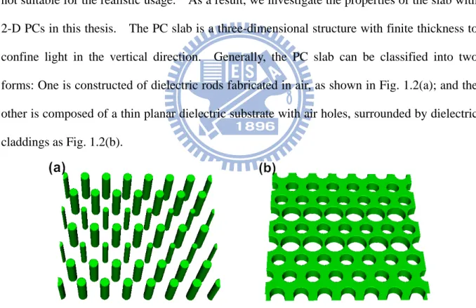
Because the design and the fabrication of two-dimensional (2-D) PCs are easy, researches and applications are mainly about 2-D PC structure. The DCs are frequently assumed with infinite height; however, a simply 2-D structure cannot strictly confine the radiation energy loss of vertical direction. Besides, a 2-D PC device with infinite height is not suitable for the realistic usage. As a result, we investigate the properties of the slab with 2-D PCs in this thesis. The PC slab is a three-dimensional structure with finite thickness to confine light in the vertical direction. Generally, the PC slab can be classified into two forms: One is constructed of dielectric rods fabricated in air, as shown in Fig. 1.2(a); and the other is composed of a thin planar dielectric substrate with air holes, surrounded by dielectric claddings as Fig. 1.2(b).
Fig. 1.2 Two types of PC slabs: (a) dielectric rod type and (b) air-hole type.
The coupler made of two identical PCWs supports two dispersion curves, with an even mode and an odd mode, respectively. It is called a symmetric DC. Two dispersion curves of a symmetric DC with triangular lattice should cross. The crossing point is called the decoupling point with infinite coupling length [17]. When an EM wave propagates at the
frequency of the decoupling point, energy is never couple into the other waveguide [18]. While the DC is designed as a demultiplexer or a switch, to decouple two waveguides might be necessary sometimes. Therefore, as designing a DC, tuning the crossing point and the dispersion relation to get the proper coupling length at the wanted range of frequencies is an important issue [19].
Although the PCWs of a DC are usually made by removing dielectric rods or air holes due to less scattering loss caused by the structure disorder [8] and easier to be fabricated, the PCW made by removing rods or holes usually guides multimodes and the coupling length are quite long [9,10]. In order to prevent from multimode propagation at the operation frequency or to reduce the coupling length, a DC made by reducing the radius of the dielectric rod or enlarging the radius of the air hole seems to be a better choice if the structure disorder can be minimized.
Besides, dispersion curves of the symmetric DC usually cross in the triangular lattices, but rarely cross in the square lattices. This phenomenon causes restrictions as designing the DC. In order to solve such problems, we adjust the DC by shifting defects of the PCWs to tune the dispersion relation and find a design rule for designing the coupler.
Applying the PWEM can derive the band diagram of the DC. And from the FDTD method, we can get characteristic of EM waves propagating within the PC. These two methods are regularly utilized to simulate a periodical PC structure. However, such numerical methods cannot provide a useful analytical result for realizing the coupling properties of the coupler or PCWs. The tight-binding theory (TBT) [20,21], which provides analytic equations, can be applied to illustrate the coupling effects between near defects of PCWs and to infer the shift trend of dispersion curves as shifting defects of the coupled PCWs. We anticipate using the TBT to derive an analytic description to explain physical properties of the PC coupler.
1-6
Organization of the thesis
In this thesis, we first introduce the extended TBT to describe the dispersion relation of a single PCW and the coupled PCWs made of slab in Chapter 2. Second, by transversely and longitudinally shifting all defects in DCs, we survey variations of coupling coefficients and their influences on the dispersion curves using the TBT. From the analytical derivation, we acquire the designing rules to tune the eigenfrequency of the decoupling point and the coupling length by suitably shifting line defects (PCWs) in Chapter 3. Finally, numerical simulations based on the PWEM and the FDTD verify the validity of the analytical results derived from the TBT for the PC couplers. The conclusion and the perspectives will be presented in Chapter 4.
Chapter 2 Theoretical Analysis
2-1
Tight-binding theory
The tight-binding theory (TBT) was first used to study the electronic properties in solid-state physics [22]. In an atom, electrons are tightly bound to the nucleus. As the separation between atoms is too close comparing to the lattice constant of the crystal, their wavefunctions overlap. Considering two atoms moving approaching, the Coulomb interaction between the nuclei and the electrons splits the energy levels, therefore energy bands result. The width of the band is proportional to the intensity of the overlap interaction between atoms. This analysis mode is closely related to the linear combination of atomic wavefunctions, and interactions between different atomic sites are considered as perturbations. The approximation method typically be used for calculation of the electronic band structure from wavefunctions of free atoms in solid-state physics is called the tight-binding approximation.
The TBT provides a straightforward way to analyze the atomic energy band structure. Recently, the TBT was also successfully used for various photonic structures. The theory can be applied to describe coupling effects between PCWs in the coupler. In this chapter, the TBT is used to analyze couplings between neighboring defects of two different types of DCs.
2-2
TBT in the dielectric rod slab
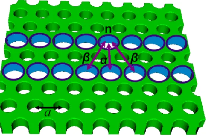
Considering a TM wave propagating in a PCW, which is consists of one line defect of reduced rods in a square lattice. The slab is made of dielectric rods with finite height fabricated in air. The lattice constant of the PC is a, as in Fig. 2.1.
Fig. 2.1 The geometric structure of a single PCW dielectric rod slab with the lattice constant a. Pm’s are the coupling coefficients between defects within a single waveguide slab.
From the extended TBT, the electric field in the waveguide can be written as the superposition of the electric field E0(r) of point defects at different sites, therefore, the time
evolution of field amplitude (u ) at the n-th site of the PCWi (i=1,2) can be expressed in ni terms of coupling with electric fields of neighbor sites [17]
2 3 0 0 1 1 i uin ( C ui) ni j m C umij( n mj un mj ). t
ω
= = + − ∂ = − − + ∂∑ ∑
(2.1)Here ω0 is the eigenfrequency of a point defect, 0
i
C represents a small shift of a localized mode due to the perturbation of the dielectric constant in both PCWs on the site n, and Cmij
being the coupling coefficient between the site n of the PCWi and the site n+m of the PCWj, defined as ,n ,n+m 2 2 0 ,n ,n d (r) i i j ij m i i C d ω ν ε ν μ ε ∞ −∞ ∞ −∞ ⋅ = ⎡ + ⎤ ⎢ ⎥ ⎣ ⎦
∫
∫
E E H E + . (2.2)Here Ei,n and Ej,n+m indicate electric fields of the site n in the PCWi and the site n+m in the PCWj, respectively, and Δε(r) is the difference between perturbed and unperturbed dielectric constants.
First let us start with a single PCW only. Let u t1n( )=U ikna i t0( − ω1 ) , the eigenfrequency of a single PCW can be expressed as
3 1 0 0 1 ( ) 2 mcos( ), m k P P mka ω ω = = − −
∑
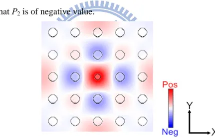
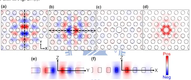
(2.3) where P0 =C0ij causes the relative frequency shift for all wavevector k from ω0, and Pm=Cmijmake the sinusoidal modulation of dispersion relations. From the electric field distribution of the point defect calculated by the PWEM, we can obtain Fig. 2.2. Ex and Ey are too small
to influence the coupling effects that can be neglected, therefore, we only consider the influence of Ez. Ez is mainly localized around the dielectric defect rod. In the z
polarization, the electric field has opposite sign when extending to the nearest neighbor rod in the x direction, i.e., E0z(r) E0z(r±ax) < 0. In order to support only a single guided mode in
the PBG, one reduces the radius or the refractive index of the defect rod, thus Δε is negative. Since Δε < 0 for rod defects, P1 is positive from the definition of Eq. (2.2). With similar
method can derive that P2 is of negative value.
Fig. 2.2 The z-polarization of the electric filed (Ez) of a point defect localized at the center of
the square lattice PC slab.
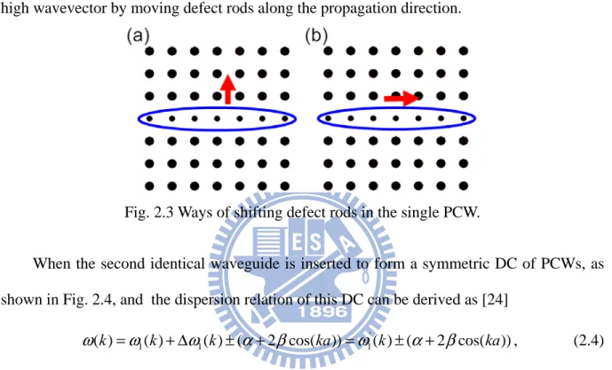
Before further consider shifting the PCW and DC either transversely (along the ±y direction) or longitudinally (along the ±x direction), first, study the effect of shifting a dielectric-rod point defect along the ±y (or ±x) axis. We could expect that due to the electric field being less localized in the dielectric region [23], the eigenfrequency (ω0) will blue shift
as the defect rod progressively moved away from the center.
eigenfrequency of the point defect increases but the electric field distribution along the propagation direction is almost unchanged. Therefore, the dispersion curves just blue shift. However, as shifting the single line defect along the x direction, shown in Fig 2.3(b), both ω0
and P0 would be increased but only slightly change the Pm’s. Hence, we could expect that
the dispersion curve is almost unchanged at the small wavevector and slightly increases at the high wavevector by moving defect rods along the propagation direction.
Fig. 2.3 Ways of shifting defect rods in the single PCW.
When the second identical waveguide is inserted to form a symmetric DC of PCWs, as shown in Fig. 2.4, and the dispersion relation of this DC can be derived as [24]
' 1 1 1
( )k ( )k ( ) (k 2 cos(ka)) ( ) (k 2 cos(ka))
ω =ω + Δω ± α+ β =ω ± α+ β , (2.4) where α =C012 =C021 and β =C±121 =C±211 are the coupling coefficients of the PCW induced by the nearest-neighbor and the next-nearest neighbor defect rods of the other PCW; ω1 and ω
are the eigenfrequencies of the single PCW and the DC, respectively. Δω1 is caused by the
difference of the coupling coefficients within single waveguide when the second PCW is inserted. Generally, Δω1 is small, we therefore neglect this term in the following discussion.
In the two PCWs coupler, the single guided mode for one PCW is split into two modes. The plus sign stands for the odd mode and the minus sign stands for the even mode. From derivations of Eq. (2.4) can obtain that two dispersion curves with different parities is crossing at k=[cos ( 2−1 − β α)] a if 2β α > [17]. Enlarging (or reducing) the distance 1 between two line defects will decrease (or increase) α and β due to different field distribution
of defects. Hence tuning coupling coefficients can tune the coupling length of a DC made of dielectric rods.
Fig. 2.4 The geometric structure of a double PCWs dielectric rod slab, here α and β are the coupling coefficients between waveguides.
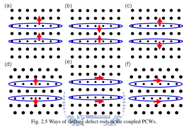
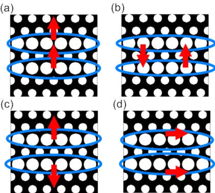
As simultaneously shifting double line defects of the DC along the y direction, shown in Fig 2.5(a), we would expect a larger ω1 because the defects moved away from the center of
the waveguide. Besides, the coupling coefficients, α and β, are almost unchanged because the separation between two PCWs is fixed. Therefore, the dispersion curves of the DC would only blue shift and the coupling lengths are still similar. As increasing the separation between two PCWs, shown in Fig. 2.5(b), α and β would become smaller, thus two dispersion curves would shift together and toward the higher frequency. On the contrary, reducing the distance between two PCWs, shown in Fig. 2.5(c), one increases the separation of the dispersion curves and both of which shift to the higher frequency. Shifting defect rods in the triangular lattice DC [see Fig. 2.5(d)] show similar properties to the square lattice DC. In the square lattice DC, the ratio of the coupling coefficients 2β α is less than one so that there would be no decoupling point. Moving the defect rods along the propagation direction in a square lattice DC, shown in Fig. 2.5(e), will also change the coupling effect. As shifting in the x direction further, we expect that the structure would become similar to the triangular
lattice, therefore, the value of 2β α gradually increases and finally two dispersion curves start crossing, just like the dispersion relation of a triangular lattice DC. Conversely, shifting the defect rods along the x direction in a triangular DC [see Fig. 2.5(f)] decreases the ratio of
2β α and finally the decoupling point disappears.
Fig. 2.5 Ways of shifting defect rods in the coupled PCWs.
2-3
TBT in the air-hole slab
In this section, the other type of slab that consists of air holes is discussed. Considering a PCW made of thin slab with triangular lattice, the air holes in the PCW are enlarged to support a single propagation mode as shown in Fig. 2.6. The lattice constant of the PC is a.
Fig. 2.6 The geometric structure of a single PCW slab made of air-hole with the lattice constant a. Pm’s are the coupling coefficients between air-hole defects within a single
waveguide.
Similar to the derivation of the dielectric rods PCW in Section 2-3, the dispersion relation of a single air-hole PCW can be presented as
3 1 0 0 1 ( ) 2 mcos( ) m k P P mka ω ω = = − −
∑
. (2.3) Assuming a TE wave is propagates in the PCW. From the electric field distribution of the point defect obtained by the PWEM, shown in Fig. 2.7, Ez is much smaller than Ex and Ey.And Ex and Ey are mainly localized at the connections between two air holes. Because Ex
seems to be quadrupole as extending in the x direction to the nearest-neighbor unit cell [see Fig. 2.7(a)], contribution to the coupling coefficients of single PCW from the overlap integration of E0x(r)E0x(r±ax) cancel out to each other and become quite small. Therefore, it
has minimal contribution to the dispersion of the PCW, but it plays an important role in waveguide coupling that will be discussed later. Furthermore, the electric field of the y-polarization in Fig. 2.7(b) has opposite sign as it extends to the nearest-neighbor unit cell in the x direction, i.e., E0y(r) E0y(r±ax) < 0, thus, P1 is positive from the definition of Eq. (2.2)
resulting from Δε <0 for air defect. Similarly, P2 can be shown also positive.
Next, consider the effect of shifting an air-hole point defect along the ±y (or ±x) axis. We could expect that the eigenfrequency (ω0) of a point defect increases as transversely or
the dielectric region between the defect hole and the nearest neighbor air holes. As shifting the defect hole, the area of the dielectric substrate between the defect hole and the nearest hole is reduced, thus making the electric field extends to the air region. Such less concentration of the electric field in the dielectric substrate causes a buleshift of the frequency when the defect hole moved away from the center. By plotting the electric field distributions of Ex and
Ey for the cross section views along the dash lines in Fig. 2.7(a) and (b), we found the electric
field is localized in the dielectric connection regions (besieged by squares) as mentioned above; and the Ex field is less localized along the y-axis in Fig. 2.7(e) than Ey one along the
x-axis in Fig. 2.7(f).
Fig. 2.7 (a) Ex, (b) Ey,(c) Ez and (d)
2
E of a point defect localized at the center. (e) (f) are the field distributions of the dash lines of (a)(b), respectively. The squares in (e) and (f) indicate the dielectric connection regions.
As shifting all the air-hole defects in the single PCW along the y direction, as shown in Fig. 2.8(a), the eigenfrequency of the point defect will increase but the electric field distribution along the waveguide direction might not changed evidently because the structure still with symmetry. One would expect all the coupling coefficients Pm are similar to the
values before shifted due to almost unchanging in field distribution as the PCW shifting along y direction. The shifting only causes the dispersion curve of the single PCW moving toward the higher frequency.
On the other hand, as moving the air-hole defect along the x direction, shown in Fig. 2.8(b), both ω0 and P0 are increased thus the dispersion curve basically locates at the same
frequency due to the smooth envelope of the electric field at low wavevectors. Under this circumstance, the perfect PCs surrounding the PCW can be effectively considered as two uniform slabs so that the propagation frequency will not be modified as the defect moved along within the uniform slabs. At large wavevector, the fast envelope distributed in periodic air and dielectric in the PCW makes more electric field distribute to the air region that cause the dispersion curves will bend toward the higher frequency at high wavevector.
Fig. 2.8 Ways of shifting the defect holes in the single PCW.
Inserting the second identical air-hole PCW on the slab separated by one partition row of air holes to the first PCW, shown as Fig. 2.9, a DC can be made.
Fig. 2.9 The geometric structure of a double PCWs air-hole slab with the lattice constant a.
α and β are the coupling coefficients between waveguides. The dispersion relation of the air-hole DC can be derived as
1
( )k ( ) (k 2 cos(ka))
the same as the eigenfrequency of dielectric rod DCs discussed in Section 2-2. In the two air-hole waveguides coupler, the single guided mode for one PCW is split into two modes. The plus and the minus signs stand for the odd and the even modes, respectively. Changing the separation between two PCWs will lead to variations of the coupling coefficients. Therefore, we can tune the coupling lengths and the frequency of the decoupling point of an air-hole DC.
As simultaneously shifting two PCWs of the DC along the y direction, as shown in Fig. 2.10(a), we expect increasing ω1 because the air-hole defects moved into the high-field
regions; however, α and β are almost unchanged as a result of fixed separation between two PCWs. Therefore, the dispersion curves of the DC should only show a blueshift with similar coupling lengths. Reducing the distance between two PCWs of the DC, shown in Fig. 2.10(b), will not only increase the electrical potential so to raise the eigenfrequency but also enhance α and β. The enhancement of waveguide coupling moves the dispersion curves apart as moving these two PCWs closer that shorten the coupling length. If one moves two PCWs apart symmetrically, shown in Fig. 2.10(c), contrarily, the coupling coefficients α and
β should become small. Thus, the coupling length increases and the dispersion curves will also shift toward the higher frequency.
On the other side, as we simultaneously shift two PCWs of the DC along the x-direction or longitudinally, as shown in Fig. 2.10(d), we expect that contribution from Ey field
distribution would dominate the influence on coupling coefficients and causethe larger value of |2β /α | after moving the defect holes along the propagation direction. Therefore, as moving the defect along the propagation direction, the decoupling point will move toward the higher wavevector.
Chapter 3 Simulation Results and Discussion
3-1
Shifting dielectric rod defects in the photonic crystal slab
An air-hole formed defect waveguide has two mechanisms of the light confinement: effects of the PBG and the index-guiding. Instead, there is only one bandgap effect of a dielectric rod waveguide needs to be considered; therefore it is simpler to analyze. Thus, simulation results of the dielectric rod type are discussed first in this chapter.
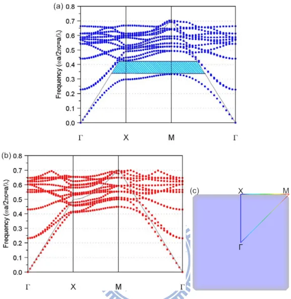
In the dielectric rod type structure, a TM polarization is easier to generate the PBG, as shown in Fig. 3.1. In the case of a PC slab, due to the lack of the translational symmetry in the vertical direction, there is no purely TE or TM mode, but rather the TE-like (even) or the TM-like (odd) mode. The band diagram of a PC slab possesses a light line. When the fields are spatially bounded, such as being localized around the defects, then the frequencies form a discrete set. The propagation modes, which under the light line are discrete because their energy is localized within the PCW, called as the guided modes. The region above the light line corresponds to the continuum of the extended modes. Modes in this region will radiate the energy outward, called the radiation modes. In the application of optical communications, we mainly consider the guided modes only.
In this section, the PWEM and the FDTD method are used to simulate and to design the PC slab with the radius of rods and the height being 0.2a and 2a, respectively, where a is the lattice constant of the crystal. The radius of the defect rods is 0.13a in both square and triangular lattice lattices. The dielectric constant of the dielectric rods is 12, which corresponds to dielectric constant of silicon at 1.55μm [see Fig. 3.2].
Fig. 3.1 Dispersion relations of a perfect dielectric rod PC slab with square lattices of the (a) TM-like (the magnetic field polarized along the waveguide) and the (b) TE-like EM waves. The gray line indicates the light line, and the shade region is the PBG. (c) The 1st Brillouin zone for a square lattice with the irreducible zone.
3-1-1 Shifting a point defect
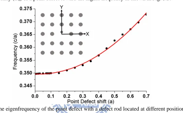
First, making the PC different from symmetry by tuning the location of a point defect away from the original center and investigates the influence on the eigenfrequency. Moving the point defect along the ±y (or ±x) direction in the square lattice will shift the eigenfrequency (ω0) of a point defect toward the higher frequency as shown in Fig. 3.3.
Fig. 3.3 The eigenfrequency of the point defect with a defect rod located at different positions along the y-axis.
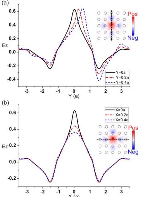
The electric field mainly localized in the dielectric rod when there is no shift of the defect. As shifting the defect rod away from the center, the portion of fields localized at the dielectric region is reduced, thus the electric field extends to the air region. Figure 3.4(a) shows how the field distribution varies with the shift degree of the defect along y-axis. The less concentration of the electric field in the dielectric substrate makes a buleshift [23]. And in Fig. 3.4(b), there is almost unchanged of the field distribution along the x-axis.
Fig. 3.4 The electric fields of the point defect made of a dielectric rod along the (a) y-axis and the (b) x-axis. The defect rod is gradually shifted toward the y direction.
3-1-2 Shifting a line defect
Next, we will investigate a PC slab with all line defects moving along the y-axis in the square lattice. The result shown in Fig. 3.5(a) indicates that the dispersion curves shift completely to the higher frequency, which suggests that the coupling coefficients Pm between
defect rods are unaffected as shifting the line defects. The frequency shift is primarily dominated by the variation of eigenfrequency (ω0) of the point defect as moving the rod.
presented in Fig. 3.5(b). The dispersion curve bends down in large wavevectors. This is due to the reason that both ω0 and P0 would increase and cancel out the effect of changing the
eigenfrequency ω1 in the section of small wavevectors. Shifts of dispersion curves merely
change apparently when the higher-order terms Pmcos(mka) become important.
Fig. 3.5 Dispersion curves of a single waveguide slab with all the defect rods are moved toward the (a) y and (b) x directions.
3-1-3 Shifting line defects of directional couplers in triangular and square
lattices
In this section we will discuss the effects as changing the separation between two PCWs of the slab. Transversely shifting two defect rows gets Fig. 3.6, which shows how the dispersion relation varies as changing the structure of the DC. Here, we discuss the square lattice structure first. Assimultaneously moving two line defects off the center and keeping the separation between PCWs fixed, we find that the dispersion curves shift toward the higher frequency, as shown in Fig. 3.6(a). In addition, the separation of the two dispersion curves does not change, i.e., the coupling length keeps fixed. On the other hand, reducing the separation of two line defects to decrease the coupling between PCWs pushes the dispersion curves apart (see Fig. 3.6(b)), and thus increases the coupling length. However, symmetrically enlarging the separation of the waveguides not only shifts the dispersion curves toward the higher frequencies but also makes two dispersion curves closer (see Fig. 3.6(c)).
Fig. 3.6 Dispersion relations of the shifted DCs, whose defect rods are moved transversely (a) with fixed separation, (b) to approach and (c) to apart from each other.
Transversely shifting two PCWs of a DC in the triangular lattice and keeping the separation fixed, one gets the dispersion relation as in Fig. 3.7. At the wavevector smaller than that of the decoupling point, two curves of the odd mode and the even mode show blue shifted with the coupling length unchanged, similar as the result of Fig. 3.6(a). Generally, tuning PCWs of a DC in the square and the triangular lattices, we will obtain alike conclusions, therefore, discussions of other conditions are abbreviating in this section.
Fig. 3.7 The dispersion relation of a triangular lattice DC with two defect waveguides are shifted transversely with fixed separation.
Besides the two dispersion curves of the symmetric DC cross at one point, there are other phenomena. The frequency of the even mode is higher than that of the odd mode for lower wavevector. As the wavevector becomes higher than the decoupling point, the odd mode owns higher frequency, namely, mode switch occurs at the decoupling point, as shown in Fig. 3.8.
Next, we inspect the results of shifting all defect rods longitudinally in Fig. 3.9. In the square lattice structure, there is no decoupling point [see Fig. 3.9(a)]. After longitudinally moving line defects, two dispersion curves come approaching to each other. When gradually shifting the defect rods, two dispersion curves begin to cross at one point at high frequency. As rods keep on moving further, the decoupling point will move toward the lower frequency or the smaller wavevector k. Conversely, in the triangular lattice DC, the decoupling point moves toward the higher frequency or the larger wavevector k and eventually two dispersion curves do not cross [see Fig. 3.9(b)]. Whether the dispersion curves cross or not depends on the coupling strength, as mentioned in Section 2-3, only when the ratio 2β α >1 [see Fig. 3.10] that the decoupling point will appear at the wavevector k=[cos ( 2−1 − β α)] a.
Fig. 3.9 Dispersion relations of shifting double defect rod channels longitudinally in the (a) square lattice and the (b) triangular lattice PC slabs.
Fig. 3.10 The values of (a) α, β and (b) 2β α as defect rods shifted in x direction in a square lattice DC.
3-2
Shifting air-hole defects in the photonic crystal slab
Because an air-hole slab is relatively simple to fabricate, this type of DCs has become the most widely used in the practical devices. In PC slab waveguides, not only the PBG provides a mechanism to restrict light propagating in the channel, but also the air-claddings provides better confinement to decrease the radiation loss during the light propagation [25].
Hence, in this section we will simulate the DC slab composed of a thin planar dielectric substrate with air-holes and surrounded by air.
In the air-hole DC, the electric fields of TE polarized light are localized in the dielectric substrate to create a bandgap; the comparative result is in Fig. 3.11.
Fig. 3.11 Dispersion relations of a perfect triangular lattice air-hole PC slab of the (a) TE-like and the (b) TM-like polarization incident EM waves, and (c) the 1st Brillouin zone for a triangular lattice with the irreducible zone.
With the intention to obtain a larger PBG, an air-hole slab is usually arranged with triangular lattice. From the simulation data of Fig. 3.12, we can clearly find that there is almost no PBG in the square lattice air-hole slab. Therefore, in the following simulations,
we only did on the air-hole PC slab with triangular lattice encircled by air. T he radius of the air holes, the thickness and dielectric constant of the slab are 0.3a, 0.55a and 12, respectively. The radius of the defect hole in the waveguide is 0.44a.
Fig. 3.12 Dispersion relations of a perfect air-hole PC slab with square lattices. The incident EM wave is TE polarization.
3-2-1 Shifting a point defect
We will consider the shift in the eigenfrequency and the redistribution of the electric field in this section upon shifting the point defect along the ±y (or ±x) axis in the triangular lattice PC slab. The eigenfrequency (ω0) blue shifts as the defect hole progressively moved
away from the center shown in Fig. 3.13. Due to the localization nature of Ey polarization,
the field distribution has less influence or is inert subjected to displacement of the defect hole than that of the extended Ex component as shown in Fig. 3.14(a) with maximum Ex(0.6a) ~
0.15 (ΔEx ~ 0.1 on moving defect) and in Fig. 3.14(d) with maximum Ey(0.8a) ~ 0.3 (ΔEy ~
0.3 on moving defect). On the other hand, the smaller change of the extended or smoother Ex field as moving the defect hole leads to less variation of eigefrequency of the shifted point
Fig. 3.13 The eigenfrequency of the air-hole point defect located at different positions shifted along the y and x axes, respectively.
Fig. 3.14 (a) Ex and (b) Ey of an air-hole point defect shifted toward the y-axis at z=0 plane.
(c) Ex and (d) Ey of an air-hole point defect shifted toward the x-axis at z=0 plane.
3-2-2 Shifting a line defect
From the results done by the PWEM, we found the dispersion curves of an air-hole PC slab shift toward the higher frequency as moving all line defects along the y-axis. The result shown in Fig. 3.15(a) indicates that the dispersion curves shift toward the higher frequency that are primarily dominated by the variation of eigenfrequency (ω0) of the point defects as
moving the hole. The dispersion curves of different y-shifted PCWs show basically parallel to one another except for that of the PCW having y > 0.1a. As keeping on shifting further,
the defect hole is close to the nearby hole and there is no sufficient space to allow the electric field wholly localized in the dielectric region. Therefore, the electric field will overflow to the air region that makes the high-order coupling coefficient P2 become larger than P1.
Since the sign of P2 and P1 are both positive the dispersion curve should bend down under
this circumstance. The results of longitudinally moving defect holes along the x-axis are presented in Fig. 3.15(b). The slope of a dispersion curve, which is the group velocity and defined as dϖ dk, slightly increases with the extent of shift. This trend is mainly due to the increase of P1 that leads this term P1cos(ka) in Eq. (2.3) affecting the eigenfrequency ω1.
Fig. 3.15 Dispersion curves of a single PCW air-hole slab with all the defect holes shifted toward the (a) y and (b) x directions.
3-2-3 Shifting line defects of directional couplers
In this section, we will simulate different conditions of transversely moving two line defects. Figure 3.16 shows how the dispersion curves vary with altering the separation of two line defects. Simultaneously shifting two rows of air-hole defects away from the center and keeping the distance between two PCWs fixed, we obtain that the dispersion curves are shifted toward the higher frequency, as shown in Fig. 3.16(a). The dispersion curves of the DC only blue shift with similar coupling lengths. And the decoupling point also keeps at the same wavevector due to the value of 2β α is not changed [see Fig. 3.17] but its eigenfrequency blue shifts accordingly. Next, by reducing the separation of two line defects symmetrically to increase the coupling coefficients between PCWs, dispersion curves will shift apart, i.e., the coupling length decreases, and the decoupling point shifts toward the higher wavevector [see Fig. 3.16(b)] since the value of 2β α becomes smaller [see Fig. 3.18], whereas, enlarging the separation of two line defects will give the opposite trend, as shown in Fig. 3.16(c) and Fig. 3.19.
Fig. 3.16 Dispersion curves of the shifted DCs, whose defect holes are moved transversely (a) with separation fixed, (b) to approach, and (c) to apart from each other.
Fig. 3.17The values of (a) α, β and (b) 2β α as defect holes shifted simultaneously in the y direction.
Fig. 3.18The values of (a) α, β and (b) 2β α as defect holes shifted to approach in the y direction.
Fig. 3.19 The values of (a) α, β and (b) 2β α as defect holes shifted to apart from each other in the y direction.
Second, we investigate the influence of moving all defect holes along the x direction. After longitudinally shifting double line defects, two dispersion curves move toward the higher frequency [see Fig. 3.20] and the decoupling point also moves toward the higher wavecector. As gradually shifting the air-hole defects, two dispersion curves finally no longer cross due to 2β α ≤1 [see Fig. 3.21]. Contribution from Ey field dominates the
Fig. 3.20 Dispersion curves of moving all the defect holes along the x direction in the triangular lattice DC.
Fig. 3.21The values of (a) α, β and (b) 2β α as defect holes shifted in x direction in the triangular lattice DC.
3-3
Coupling lengths calculated by the FDTD method
In this section, we anticipate obtaining the EM waves propagating conditions in the DC by the FDTD method by considering an EM wave with frequency 0.37264c/a is incident into the dielectric rod DC with square lattice, as shown in Fig. 3.22(a). Without shifting the PCWs, the coupling length is approximately equal to 18.8a [see Fig. 3.22(b)]. As
transversely shifting two defect waveguides 0.2a closer, the coupling length reduces to 8.2a [see Fig. 3.22(c)]. The coupling lengths derived by the FDTD method are consistent with the results calculated by the PWEM [see Fig. 3.23].
Fig. 3.22 (a) A dielectric rod DC with square lattice. Propagating EM waves in two waveguides (b) without any shift and (c) transversely shifted 0.2a closer.
Next, we survey the conditions of an EM wave transfers in the air-hole DC, the device structure is shown as Fig. 3.24(a). The frequency of the incident wave is 0.285c/a having the coupling length of about 3.5a [see Fig. 3.24(b)]. As shifting the defect rows 0.1a closer to each other, the coupling length reduces to 4.6a [see Fig. 3.24(c)]. Comparing the results of the PWEM, as shown in Fig. 3.25, the FDTD method obtains similar coupling lengths.
Fig. 3.24 (a) The air-hole DC with triangular lattice. Propagating EM waves in two waveguides (b) without any shift, (c) transversely shifted 0.1a to apart from each other.
Chapter 4 Conclusion and Perspectives
4-1
Conclusion
We have demonstrated that the electric field will propagate in the incident channel without leaking into another as the incident frequency is chosen at the decoupling point. By moving off the defect rods or holes, we can efficiently change the dispersion curves, and thus modify the coupling length and the decoupling frequency. As the defect rows are moved away from the center, dispersion curves blue shift. Two dispersion curves get apart or closer by decreasing or enlarging the separation of the coupled PCWs in both triangular and square structures of the PC devices. Shifting defect waveguides would change the magnitude of the coupling coefficients of the first (α) and the second (β) nearest-neighbor defects of the DC, therefore modifies the coupling length and the location of the decoupling point. Longitudinally moving two PCWs along the wave propagating direction also changes the ratio of the coupling coefficients, therefore shifts the decoupling point of a triangular-lattice DC toward the higher wavecector and two dispersion curves of a square-lattice DC cross. By using of these properties, we can design the decoupling point for a certain operation frequency, no matter the DC is made of dielectric rods or air-holes. Finally, the TBT successfully explains these coupling properties that can be confirmed by the PWEM and the FDTD method and provides a designing rule for the photonic crystal slab couplers in optical integrated circuits.
4-2
Prospectives
In this thesis, we have discussed the coupling effects of DCs without considering optical nonlinearity. The characteristic of nonlinear DCs is also a considerable topic, e.g., the
optical Kerr effect provides possible tuning the refractive index of the dielectric material in respond to an applied electric field. The dispersion relation of a defect waveguide in the nonlinear PC structure is different from that in the linear medium. Utilizing this characteristic we can design the DC as an active component. When an EM wave is incident into the nonlinear DC devices, the propagating condition can be tuned corresponds to the intensity of the input field. With this notion, the active-DC can serve as a logic gate in optical integrated circuits. Therefore, knowing the properties of a nonlinear DC are interesting and useful issues in integrated optics.