國
立
交
通
大
學
電機學院 IC 設計產業研發碩士班
碩
士
論
文
砷化銦/砷化鎵量子點紅外線偵測器陣列之低溫互補式
金氧半讀出積體電路設計與分析
THE DESIGN AND ANALYSIS OF CRYOGENIC CMOS READOUT INTEGRATED
CIRCUIT FOR InAs/GaAs QUANTUM-DOT INFRARED DETECTOR ARRAY
研 究 生:謝仲朋
指導教授:吳重雨 教授
砷化銦/砷化鎵量子點紅外線偵測器陣列之低溫互補式金氧半讀出
積體電路設計與分析
THE DESIGN AND ANALYSIS OF CRYOGENIC CMOS READOUT
INTEGRATED CIRCUIT FOR InAs/GaAs QUANTUM-DOT
INFRARED DETECTOR ARRAY
研 究 生:謝仲朋 Student:Chung-Peng Hsieh
指導教授:吳重雨 Advisor:Chung-Yu Wu
國 立 交 通 大 學
電機學院 IC 設計產業研發碩士班
碩 士 論 文
A ThesisSubmitted to College of Electrical and Computer Engineering National Chiao Tung University
in partial Fulfillment of the Requirements for the Degree of
Master in
Industrial Technology R & D Master Program on IC Design
February 2006
Hsinchu, Taiwan, Republic of China
砷化銦/砷化鎵量子點紅外線偵測器陣列之低溫互補
式金氧半讀出積體電路設計與分析
學生:謝 仲 朋
指導教授:吳 重 雨 博士
國立交通大學
電機學院
IC 設計產業研發碩士班
摘要
本論文提出並分析低溫(Cryogenic)互補式金氧半(CMOS)讀出電路設計以製作運用 在砷化銦/砷化鎵量子點紅外線偵測器陣列光訊號讀出之積體電路晶片。讀出電路為紅 外線影像系統中偵測器陣列與後級訊號處理間的重要介面電路。為運用矽半導體元件電 路之優良特性與匹配紅外線偵測器材質之低溫工作環境,我們提出了可工作在低溫環境 下之讀出電路架構,並以互補式金氧半製程技術完成電路的設計、模擬、與晶片研製。 而所製作之讀出晶片中的優異效能與成果均已由實驗或模擬驗證。利用『緩衝式閘調變輸入』(Buffered Gate Modulation Input)讀出架構,可以改 進傳統『閘調變輸入』(Gate Modulation Input)的問題與缺點,並完成包括適應性增 益 控 制 (adaptive gain control) 與 電 流 式 背 景 壓 抑 (current-mode background suppression)功能的讀出晶片。此前級訊號處理功能(on-FPA signal processing)可以 提高讀出電路的效能並降低後級電路雜訊之影響。電流式背景壓抑更可提高訊號動態範 圍與避免積分電容飽和。雙重三角取樣(Double Delta Sampling)電路也被使用來減少 固定樣式雜訊(fixed pattern noise)、時脈回饋雜訊和通道電荷注入。一實驗性 16x16
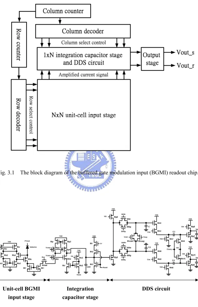
讀出晶片使用 0.35 μm 2P4M N-well 互補式金氧半技術設計並完成晶片研製,在 77K 溫 度下及 3.3 V 工作電壓,其量測結果成功驗證了讀出晶片的效能。輸出線性度為 95%、 最大輸出擺幅為 1V、最大讀出速度為 1.25 MHz、畫面速率為 4880 frames/sec、功率消 耗為 30 mW。此高效能讀出電路具有高注入效率(injection efficiency)、高動態範圍 (dynamic range)、高電荷容量(storage capacity)、低雜訊等優點,可適用於大範圍 背景亮度與高對比影像讀出的運用。
我們深信,吾人所提出之互補式金氧半讀出電路架構以及其設計技術已為紅外線影 像系統之讀出處理電路設計提供一個新方向。爾後,相關的研究發展與實際應用於不同 影像系統包括可見光與紅外線將持續進行。
THE DESIGN AND ANALYSIS OF CRYOGENIC CMOS
READOUT INTEGRATED CIRCUIT FOR InAs/GaAs
QUANTUM-DOT INFRARED DETECTOR ARRAY
Student : Chung-Peng Hsieh Advisor : Chung-Yu Wu
Department of Electronics Engineering & Institute of Electronics
National Chiao Tung University
ABSTRACT
In this thesis, a cryogenic CMOS readout structure is proposed, developed, and applied to the implementation of photon signal readout integrated circuit for InAs/GaAs quantum-dot infrared detector array. The silicon readout circuit is an important interface circuit of detector array and signal processing stage in the IR image system. To achieve high performance readout and fit the cryogenic working characteristic of IR detector material, a cryogenic CMOS readout structure has been developed and fabricated. The functions and superior readout performance of the proposed CMOS readout structure have been verified by experimental measurement under 77K environment or simulations.
By using the buffered gate modulation input (BGMI) circuit, it can improve the performance and problem of the conventional gate modulation input (GMI) with adaptive gain control and current-mode background suppression. The on-FPA signal processing capability of BGMI circuit at front stage can reduce the noise effect of downstream circuit and
improve the readout performance. The current-mode background suppression can increase the signal dynamic range and avoid integrating saturation on capacitor. Moreover, the double delta sampling (DDS) circuit is used to suppress fixed pattern noise, clock feedthrough noise, and channel charge injection. An experimental 16x16 readout chip has been designed and fabricated by using 0.35 μm 2P4M N-well CMOS technology. The measurement results of the fabricated readout chip under 77K and 3.3 V supply voltage have successfully verified both readout function and performance. It is shown that the linearity performance of the readout chip is better than 95% and the maximum output swing is 1V. The maximum readout speed is 1.25 MHz. The frame rate is 4880 frames/sec. The total active chip power is below 30 mW at 77K. It is shown that a high-performance readout interface circuit for IR FPA with high injection efficiency, high charge sensitivity, high dynamic range, large storage capacity, and low noise is realized. These advantageous traits make the readout circuit suitable for the various applications with a wide range of background.
It is believed that the proposed CMOS readout circuit and the associated design methodology offer new design scope and future feasibility for new-generation readout ICs of infrared detector array. Further improvement on circuit performance and practical applications in various image system including visible and thermal image readout will be explored and developed in the future.
致 謝
首先感謝我的指導老師吳重雨教授耐心的指導與鼓勵,使我能順利完成碩士學位。 在吳教授循序漸進的諄諄教誨下,讓我不僅獲得許多積體電路設計的專業知識,更學習 到做研究時應有的挑戰困難及解決問題的態度與方法,面對問題時如何著手構思和勇於 嘗試,雖然在過程倍感艱辛,但卻獲益良多。 其次要感謝口試委員柯明道教授、謝志成博士、林時彥博士提供許多寶貴的意見與 指導,使本論文可以更加完備。 再來要感謝中央研究院應用科學研究中心的林時彥博士、周淑婷博士在晶片規格上 的協助與建議,以及量測環境和硬體設備的支援,讓研究可以順利完成。感謝國科會晶 片設計製作中心張淑慧小姐和實驗室助理卓慧貞小姐在各項行政事務上的協助。 感謝林俐如、王文傑、虞繼堯、陳勝豪、楊文嘉、蔡夙勇、林韋霆、陳煒明等諸位 307 實驗室學長姊在各項研究上的指導。感謝實驗室同學黃必超、黃俊、廖宏泰、李允 斌、張志遠、孫汝玉、詹豪傑、羅怡凱、陳佳惠、王志賢、高立龍,和楊國忠、鄭人文、 廖廷偉等學弟們,陪我一起度過難忘的研究生活,營造互相激盪的討論風氣,不同觀點 的知識分享。 最後,我要致上最深的感謝給我的父母親,謝謝你們一直以來的支持與鼓勵,讓我 能順利完成學業。還有我的女友靜雯,謝謝妳總是能在我忙碌的時候,給予溫柔的體諒 與溫馨的支持。期望將這份喜悅與你們共享。 謝 仲 朋 誌於 風城交大 九十六年二月CONTENTS
ABSTRACT ( CHINESE ) ...i
ABSTRACT ( ENGLISH )... iii
ACKNOWLEDGMENT ...v
CONTENTS... vi
TABLE CAPTIONS ... ix
FIGURE CAPTIONS ...x
CHAPTER 1 INTRODUCTION
1.1 BACKGROUNG ... 1
1.2 MOTIVATION... 2
1.3 THESIS ORGANIZATION ... 3
CHAPTER 2 REVIEW ON INFRARED FOCAL PLANE
ARRAY AND CMOS READOUT TECHNIQUIES
2.1 STURCTURES AND OPERATIONAL REQUIREMENTS OF IR
FPA... 8
2.1.1 IR FPA Structures... 8
2.1.2 Operational Requirements for IR FPA... 10
2.2 CMOS READOUT TECHNIQUES FOR IR DETECTORS ... 15
2.2.2 Noise Reduction of IR Image ... 23
2.2.3 Double Delta Sampling (DDS) Circuit ... 24
CHAPTER 3 ARCHITECTURE AND CIRCUIT DESIGN
3.1 CHIP ARCHITECTURE ... 31
3.2 CIRCUIT DESIGN ... 32
3.2.1 Buffered Gate Modulation Input (BGMI) stage ... 32
3.2.2 The Current Mode Background Suppression Circuit... 33
3.2.3 Double Delta Sampling (DDS) Circuit ... 35
3.3 CHIP OPERATION... 36
3.4 SIMULATION RESULTS ... 38
CHAPTER 4 EXPERIMENTAL RESULTS
4.1 LAYOUT DESCRIPTIONS... 49
4.2 TESTING ENVIRONMENT ... 50
4.3 EXPERIMENTAL RESULTS AND DISCUSSIONS ... 50
CHAPTER 5 A NEW ION SENSOR CHIP
5.1 INTRODUCTION... 63
5.2 CIRCUIT DESIGN ... 64
5.3 SIMULATION AND EXPERIMENTAL RESULTS... 66
5.4 SUMMARY... 67
6.1 CONCLUSIONS ... 83
6.2 FUTURE WORK ... 84
REFERENCES
... 86
TABLE CAPTIONS
CHAPTER 3
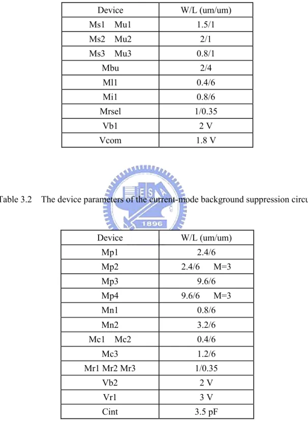
Table 3.1 The device parameters of the unit-cell BGMI input stage.
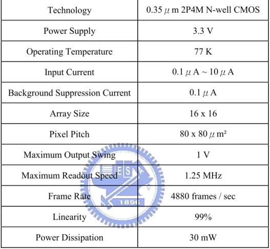
Table 3.2 The device parameters of the current-mode background suppression circuit. Table 3.3 The device parameters of double delta sampling (DDS) circuit.
Table 3.4 The simulated performance and operation condition of the readout chip.
CHAPTER 4
Table 4.1 The measured performances and operation conditions of the readout chip.
CHAPTER 5
Table 5.1 The device parameters of the telescopic operational amplifier. Table 5.2 The device parameters of the bias circuit.
Table 5.3 The simulated performances of the telescopic operational amplifier.
Table 5.4 The simulated voltage gain of the ion sensor chip with positive input voltages Vin. Table 5.5 The simulated voltage gain of the ion sensor chip with negative input voltages Vin.
FIGURE CAPTIONS
CHAPTER 1
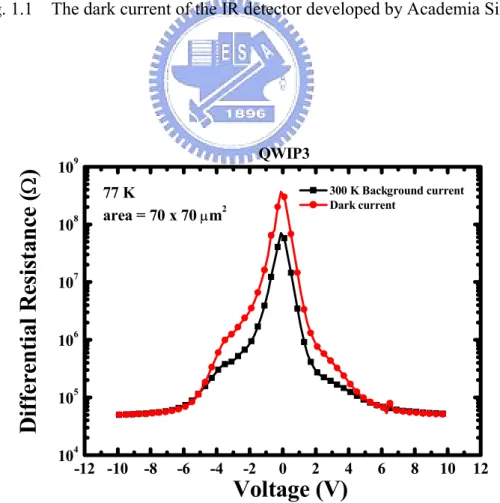
Fig .1.1 The dark current of the IR detector developed by Academia Sinica.
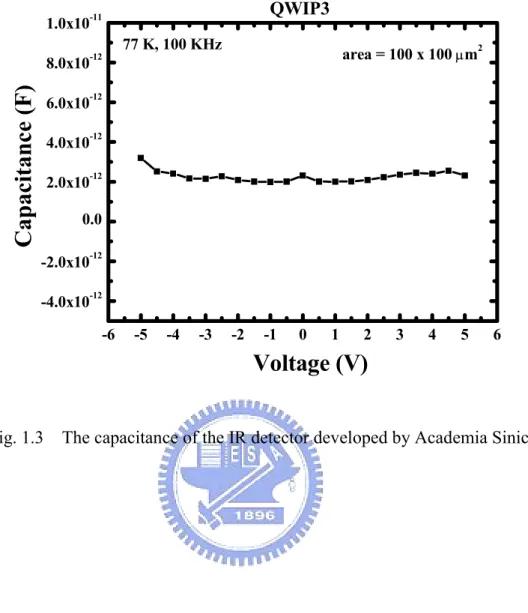
Fig. 1.2 The differential resistance of the IR detector developed by Academia Sinica. Fig. 1.3 The capacitance of the IR detector developed by Academia Sinica.
CHAPTER 2
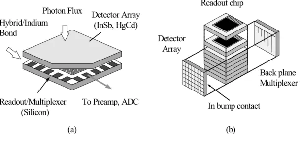
Fig. 2.1 The technologies of the hybrid array structures : (a) the flip-chip array technology; (b) the Z-plane technology.
Fig. 2.2 (a) The structure of monolithic array technology; (b) The structure of pseudo-monolithic array technology. Fig. 2.3 The source follower per detector (SFD) readout circuit. Fig. 2.4 The direct injection (DI) readout circuit.
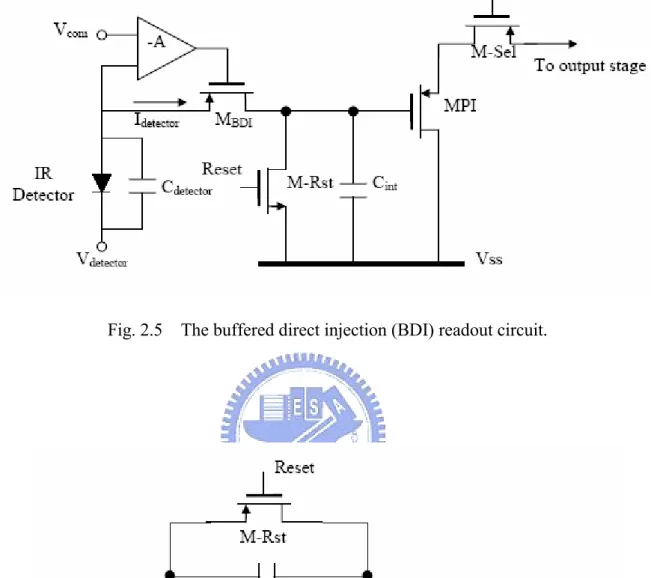
Fig. 2.5 The buffered direct injection (BDI) readout circuit.
Fig. 2.6 The capacitive transimpedance amplifier (CTIA) readout circuit. Fig. 2.7 The gate modulation input (GMI) readout circuit.
Fig. 2.8 The buffered gate modulation input (BGMI) readout circuit. Fig. 2.9 Double Delta Sampling (DDS) circuit.
Fig. 3.1 The block diagram of the buffered gate modulation input (BGMI) readout chip. Fig. 3.2 The schematic of readout circuit.
Fig. 3.3 The buffered gate modulation input (BGMI) pixel circuit.
Fig. 3.4 The shared integration cell with current-mode background suppression. Fig. 3.5 The double delta sampling (DDS) circuit.
Fig. 3.6 The 1-stage counter of the digital control circuit. Fig. 3.7 The 8-stage counter of the digital control circuit. Fig. 3.8 The decoder of the digital control circuit.
Fig. 3.9 The major timing diagram of the column readout circuit and the output driver circuit.
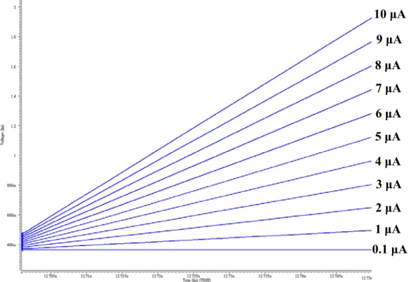
Fig. 3.10 The simulated waveforms of Vint on integration capacitor with input current from 0.1 μA to 10 μA and background suppression current 0.1 μA.
Fig. 3.11 The simulated waveforms of the voltage difference between Vout_r and Vout_s with input current from 0.1 μA to 10 μA and background suppression current 0.1 μA.
Fig. 3.12 The simulation result of 16x16 pixel array readout circuit with different input current flowing into every pixel.
Fig. 3.13 The simulated linearity of the 16x16 readout circuit at 77K.
CHAPTER 4
Fig. 4.1 The block diagram of the layout of the 16x16 readout chip. Fig. 4.2 The photograph of the fabricated 16x16 readout chip.
Fig. 4.3 The testing environment of the fabricated infrared readout chip.
the 2 frame-period with the end-of-frame signal.
Fig. 4.5 The measured Vout waveforms of the fabricated 16x16 readout chip at 77K on a single pixel Row#16 Col#16 with the end-of-frame signal.
Fig. 4.6 The measured Vout waveforms of the fabricated 16x16 readout chip at 77K under different photo current : (a) 1 uA; (b) 2 uA; (c) 4 uA; (d) 6 uA; (e) 8 uA; (f) 10 uA. Fig. 4.7 The measured linearity of the 16x16 readout chip at 77K.
Fig. 4.8 The measured linearity of the 16x16 readout chip at 300K.
Fig. 4.9 One IR photo detector is connected to a single pixel of the readout chip. Fig. 4.10 The measured output voltage Vout_r – Vout_s versus IR photo detector bias
voltage at 77K.
Fig. 4.11 The measured photo current versus IR photo detector bias voltage at 77K. Fig. 4.12 The measured photo current (log scale) versus IR photo detector bias voltage at
77K.
Fig. 4.13 The measured photo current versus IR photo detector bias voltage at 10K.
Fig. 4.14 The uniformity on 7 testing pixels of the readout chip with different input currents from 1 uA to 9 uA.
CHAPTER 5
Fig. 5.1 The test solution on the sensor surface for detecting concentration of ions. Fig. 5.2 The enzyme (imidase) reaction on the sensor surface for detecting the generated
ions.
Fig. 5.3 The architecture of the ion sensor chip.
Fig. 5.4 The schematic of the telescopic operational amplifier. Fig. 5.5 The bias circuit of the telescopic operational amplifier.
Fig. 5.6 The simulation results of the telescopic operational amplifier.
Fig. 5.7 The simulation result of the slew rate of the telescopic operational amplifier. Fig. 5.8 The simulation result of the ion sensor chip.
Fig. 5.9 The block diagram of the layout of the ion sensor chip. Fig. 5.10 The photograph of the fabricated ion sensor chip.
Fig. 5.11 The measured Vout waveforms of the ion sensor chip with C2 = 10 pF under
different input voltages Vin : (a) 1 mV; (b) 2 mV; (c) 3 mV; (d) 4 mV; (e) 5 mV; (f) 6 mV.
Fig. 5.12 The measured Vout waveforms of the ion sensor chip with C2 = 5 pF under different input voltages Vin : (a) 400 uV; (b) 1 mV; (c) 1.4 mV; (d) 2 mV; (e) 3 mV; (f) 4 mV.
Fig. 5.13 The measured Vout waveforms of the ion sensor chip with C2 = 1 pF under
different input voltages Vin : (a) 600 uV; (b) 800 uV; (c) 1 mV; (d) 1.4 mV; (e) 1.8 mV; (f) 2.2 mV.
Fig. 5.14 The corresponding voltage gain Av under different C2 : (a) 10 pF; (b) 5 pF; (c) 1 pF.
Fig. 5.15 The enzyme reaction can direct contact on the sensor surface to detect the generated ions for biology applications.
CHAPTER 1
INTORDUCTION
1.1 BACKGROUND
Infrared (IR) imaging technology has recently been finding a growing range of applications including IR search and track, medical examination [1], astronomy [2], forward-looking infrared (FLIR) systems, missile guidance, and other strategic equipment [3]. These days, the design of IR image system with multi-function is more and more valuable. For example, the integration of commercial and military IR imaging systems meets both economic and defense challenges. This concept has led to the increasing research and developments efforts in applying the commercial CMOS VLSI technologies in the design of IR imaging systems. Incorporating the rapid advancement in CMOS VLSI with the progress in infrared focal-plane array (IR FPA) technologies like detector material, sensing structure, optics, coolers, readout electronics, image enhancement, and intelligent signal processing results in the revolution of IR image systems to a new generation with significant performance improvement.
In general, the IR FPA can be divided into two major parts, namely the detector array and the readout electronics. As compared to the conventional discrete design, the IR FPA has the inherent advantages of high packing density, low cost, high feasibility on-chip signal processing, and high flexibility for system integration. In the high-sensitivity applications, the IR FPAs are typically fabricated with narrow bandgap semiconductor detectors and silicon multiplexer and operated in the cryogenic environment. Thus very challenging technologies
for detection materials and the system interface are required. Moreover, high-performance and low-temperature mixed-mode circuit design are also required for the readout electronics [4]. To achieve the optimal overall performance of the IR FPAs, suitable trade-off among circuit performance, power dissipation, chip area, and image resolution should be made. A number of readout structures have been developed for different system application and concern.
1.2 MOTIVATION
The readout circuit of infrared (IR) detector focal-plane-array (FPA) is a very important interface in the overall IR detection system. Thus, many technologies of designing readout circuit are still under development. There are various design requirements and constraints on the readout interface circuit such as charge storage capacity, noise, dynamic range, power dissipation, detector bias control, array size, and pixel pitch. As the cell number in the FPA becomes larger, the pixel size and pitch should be scaled down to accommodate more detector cells. The small pixel size limits the complexity of the input stage in the readout circuit and the storage capacitance, which may degrade the readout performance. Thus many efforts have been devoted to the developments of new techniques and circuits to improve readout performance under various constraints. By using background suppression and adaptive current control techniques, the effective storage capacity, dynamic range, and noise performance are improved.
Generally background suppression can be realized in two circuits, namely the charge domain background suppression circuit [5] and the current memory-based background suppression circuit [6]. The charge domain circuit integrates the complete signal prior to background suppression. Thus it cannot alleviate the storage capacity limit problem. On the other hand, the current memory suppression circuit needs complex in-pixel feedthrough reduction circuit and calibration cycle. Thus it is not suitable for large format FPA
applications. It is well known that the gate modulation input (GMI) circuit, can yield very low input-referred noise and high charge detection sensitivity due to the high current-mode gain. But the GMI circuit is susceptible to voltage bias noise and the fixed pattern noise (FPN) due to threshold-voltage variations. Thus, the readout performance is limited by these factors.
In this thesis, a current readout structure for IR FPA, called the buffered gate modulation input (BGMI) circuit, is used to solve the above mentioned problems and improve the readout performance. Based on the switch-current integration (SCI) readout structure, the BGMI circuit integrates the shared-buffer detector biasing technique with a GMI-like current gain configuration in the unit cell input stage. The current gain is achieved by a new unbalanced current mirror configuration which is immune from the process-dependent threshold-voltage variation. A current-mode background suppression circuit is also implemented in the off-FPA shared integration capacitor unit. Moreover, the dynamic charging output stage with the double delta sampling (DDS) is included to eliminate noise. It has been shown from both simulation and experimental results that the BGMI readout circuit can achieve good readout performance through the use of BGMI technique, the off-FPA current mode background suppression.
In this work, the BGMI readout circuit array will be combined with the InAs/GaAs quantum-dot IR detector array which developed by Academia Sinica to compose a complete IR image system. The property of the InAs/GaAs quantum-dot IR detector array is illustrated by Figs. 1.1-1.3. Fig. 1.1 shows the dark current of the IR detector. Fig. 1.2 shows the differential resistance of the IR detector. Fig. 1.3 shows the capacitance of the IR detector. The detector array and the readout circuit array will be combined with the indium bond.
1.3 THESIS ORGANIZATION
developing the readout circuit, the architecture and circuit design, the both simulation results and experimental results of the fabricated readout chip, and the conclusions and future work.
Chapter 1 introduces the background and explains the main topics of this thesis.
In Chapter 2, the architectures and operational requirements of IR FPA, and the CMOS readout techniques for IR detectors including the state-of-the-art structure are given. In this chapter, the analysis of advantages and drawbacks of the conventional gate modulation input (GMI) and buffered gate modulation input (BGMI) are given.
In Chapter 3, the circuit structure, readout strategy, and simulation results are presented. By applying BGMI technique, this readout circuit can achieve good readout performance, high charge sensitivity, and has a good immunity from threshold-voltage variations. Moreover, the readout dynamic range is dramatically increased by using a threshold-voltage independent current-mode background suppression technique. The double delta sampling (DDS) circuit is used to reduce fixed pattern noise, clock feedthrough noise, and the noise from the effect of channel charge injection. Then the chip operation and simulation results are described.
In Chapter 4, an experimental 16 x 16 BGMI readout chip has been designed and fabricated in TSMC 0.35 μm 2P4M N-well CMOS technology. The measurement results of the fabricated readout chip under temperature 77K and 3.3V supply voltage have successfully verified both readout function and performance. It has been shown that a high-performance readout interface circuit for IR FPA with high injection efficiency, high charge sensitivity, high dynamic range, high linearity, and low noise is realized within the pixel size of 80 x 80 um2. These advantageous traits make the circuit suitable for the various applications with a wide range of background current.
In Chapter 5, a new ion sensor chip for the applications of biology is proposed. An experimental ion sensor chip has been designed and fabricated in TSMC 0.18 μm 1P6M N-well CMOS technology. It has been shown from both simulation and experimental results that the proposed ion sensor structure can achieve good readout performance. The circuit
structure, readout strategy, and circuit performance of the new ion sensor structure are described first. Then both simulation results and experimental results of the fabricated ion sensor chip are presented. Finally, a summary is given.
Finally, the main results of this thesis are summarized in Chapter 6. Some suggestions for the future work about the readout circuit design are also discussed.
-10 -8 -6 -4 -2 0 2 4 6 8 10 10-12 10-11 10-10 10-9 10-8 10-7 10-6 10-5 10-4 10-3 10-2 10-1 300 K Background current Dark current area = 70 x 70 μm2
C
u
rren
t (A
)
77 KVoltage (V)
QWIP3Fig. 1.1 The dark current of the IR detector developed by Academia Sinica.
-12 -10 -8 -6 -4 -2 0 2 4 6 8 10 12 104 105 106 107 108 109 300 K Background current Dark current 77 K area = 70 x 70 μm2 QWIP3
Di
ff
eren
ti
al
Res
is
ta
nc
e
(
Ω
)
Voltage (V)
-6 -5 -4 -3 -2 -1 0 1 2 3 4 5 6 -4.0x10⁻¹² -2.0x10⁻¹² 0.0 2.0x10⁻¹² 4.0x10⁻¹² 6.0x10⁻¹² 8.0x10⁻¹² 1.0x10⁻¹¹ area = 100 x 100 μm2
Voltage (V)
Capacit
anc
e (F)
QWIP3 77 K, 100 KHzCHAPTER 2
REVIW ON INFRARED FOCAL PLANE ARRAY
AND CMOS READOUT TECHNIQUES
2.1 STRUCTURES AND OPERATIONAL REQUIREMENTS OF IR
FPA
2.1.1 IR FPA Structures
Recently, the development of IR FPA technologies has made the design of high-sensitivity, high-density, large-format, and high-spectral-resolution IR image systems quite feasible. Moreover, the progress of VLSI techniques and detector fabrication technologies dramatically reduce complexity and cost of IR systems. The application of various developed technologies on the design of IR FPAs has resulted in the advantages of simplified electrical interconnection, higher performance reliability, and simplified package. Some commonly used structures of the three major classes of IR FPAs, namely, hybrid array, monolithic array, and pseudo-monolithic array, are reviewed below.
1) Hybrid Array :
The most commonly used IR FPA structures in the hybrid array [7] are flip-chip and Z-plane technologies [8] as shown in Fig. 2.1(a) and 2.1(b), respectively. In Fig. 2.1(a), the IR detector array chip and the readout chip are compounded by the indium bump grown on the aligned pixels of both chips. This is the mostly used structure in the hybrid array technology. In the Z-plane technology shown in Fig. 2.1(b), the readout chips are stacked one on top of
another and then the detector array is mounted to the third dimensional plate on the edge. In the Z-plane structure, one readout chip is used by one channel of detectors so that many electrical circuit techniques like complex input circuit, gain offset correction, A/D converter, filter, smart and neural function, as well as image signal processing stage can be implemented on the readout chip [9]. However, the image resolution is limited by the readout chip thickness. In the application of hybrid array technology, uniformity of indium bumps, chip alignment as well as thermal expansion effect and mechanical damage on the detectors should be considered during the hybridization process [10].
2) Monolithic Array :
The monolithic array technology is developed to solve the hybrid process problems by building IR detectors like PtSi Schottky barrier [11], micromachining bolometer [12], or extrinsic detectors on the silicon substrate [13]. Thus both IR detectors and readout circuits can be fabricated in one monolithic chip as shown in Fig. 2.2(a). The reliability of IR FPAs can be improved under monolithic design. However, the detector types and materials must be compatible with the silicon process. This limits the applications of monolithic array on IR image systems.
3) Pseudo-Monolithic Array :
As an alternative method to the indium-bumping hybrid array and monolithic array technologies, the readout chip and detector chip can be compounded through the via-hole technique [14], in the so-called pseudo-monolithic array as shown in Fig. 2.2(b). Both readout chip surface and detector chip surface must be polished to achieve a precisely flatness and parallelism before combined as a single chip. Then some detector fabrication processed and routing metallization processes are applied on the combined single chip. The pseudo-monolithic technology remains some advantages of silicon-like processing, but its reliability is still needed to be optimized.
2.1.2 Operational Requirements for IR FPA [15]
In different applications of IR image systems, there exist certain specific requirements for the design of IR FPAs. In general, the requirements involve a broad range of electrical circuit and detector array parameters like detector bias control, injection efficiency, charge storage capacity, integration time, noise, dynamic range, readout rate, array size and pixel pitch, power consumption, and operating temperature. Some general discussions of these requirements are summarized below.
1) Detector Bias Control :
The dark current, injection efficiency, detector 1/f noise, and responsibility are affected by the detector bias. Moreover, operation ability and linearity of spectral response are also affected directly by the bias. Therefore, a strict and stable detector bias control is necessary in IR FPAs.
2) Injection Efficiency and Bandwidth :
The injection efficiency is defined as the ratio of the current flowing into the readout circuit to the detector current. High injection efficiency and wide input bandwidth leads to good responsibility and readout performance. To achieve high injection efficiency and wide bandwidth, the input impedance of the interface circuit should be lower than the shunt resistance of IR detectors.
3) Charge Storage Capacity :
In most readout structures of IR FPAs, the photon excited carriers are accumulated on the integrating capacitor and transferred to voltage output. Therefore, the charge storage capacity is determined by both background and dark current levels of IR detectors as well as the value of integrating capacitor. Maximum charge storage capacity can be achieved by keeping background and dark currents small and using a large integrating capacitor. However, the capacitance value is limited by pixel size and the chip area of readout circuit.
4) Noise :
Noise in the IR FPAs can be separated typically into two categories, random noise and pattern noise. Random noise varied temporally and is not constant from frame to frame in the imager. Pattern noise is divided into two components, one is fixed pattern noise (FPN) and the other is the photo-response nonuniformity (PRNU). The FPN comes from dimensions, doping concentration, and contamination of photo-detectors and the characteristics of threshold voltage, width, and length in MOSFETS. The PRNU noise comes from the thickness of layers on the top of photo-detectors and wavelength of illumination. These noises in the CMOS in the IR FPAs are briefly discussed below.
(i) Random Noise :
An imager with a constant scene should produce identical output from frame to frame. In practice, the output from a given pixel will vary over time due to thermal noise, charge trapping, and 1/f noise in the devices which comprise the imager. Photonic shot noise is usually not included in this quantity, although this also contributes to noise at the output. Random noise is typically stated in terms of input-referred equivalent electrons, i.e., the root mean square (rms) output voltage noise divided by the conversion gain.
(ii) Fixed-Pattern Noise :
Fixed-pattern noise (FPN) is the fixed (constant in time) variation between pixel outputs under spatially uniform illumination. Fixed-pattern noise is typically due to random or mask-induced mismatches in device parameters such as threshold voltage, trap density, and parasitic capacitance. FPN is usually a function of illumination, and can be written as the sum of a gain term and an offset term for an imager with a linear response characteristic. Offset FPN is constant over illumination, and gain FPN is proportional to illumination.
FPN consists of components that describe variation between columns, and variation between pixels in a single column. Column FPN is the standard deviation of the
column-average pixel output values in a time-average, uniformly illuminated frame. The column FPN is expressed as : FPN (column) = 2 ( ) 1 j j P P j − −
∑
(2.1)Where Pj is the average pixel value in column j and P is the average pixel value in the
frame. Since a column FPN calculation requires multiple columns, j > 1. Pixel FPN is the standard deviation of pixel output values after column FPN has been removed. In order to calculate pixel FPN, multiple pixels are required. The pixel FPN is expressed as
FPN (pixel) = 2 , , ( ) 1 i j j i j P P i j − ⋅ −
∑
(2.2) where i • j > 1. (iii) Reset Noise :If the diffusion of the photodiode is reset through a MOSFET, this is equivalent to a capacitance being charged through the resistance of the MOSFET channel. The rms (root-mean-square) noise voltage can be expressed as
〈Vrms〉= kT
C (2.3)
where k is the Boltzmann constant, T is temperature, and C is the capacitance of photodiode. The reset noise is generally called “KTC” noise.
(iv) Thermal Noise :
Thermal noise is due to the random thermal motion of the electrons and is unaffected by the presence or absence of direct current. It is a white noise which means the noise power is constant over all frequencies. For a resistor, the thermal noise rms voltage can be expressed as
where B is the noise bandwidth and R is the resistor. Since the thermal noise covers the entire frequency range, the bandwidth determines the actual amount measured.
(v) Shot Noise :
Shot noise is another white noise that arises from the discrete nature of the electrons, for example, the random arrival of particles of charge. This is the result of the random generation of carriers such as thermal generation within a depletion region (i.e. shot noise of dark current) or the random generation of photon-electrons, and always associated with the direct-current flow through the device.
(vi) Flicker (1/f) Noise :
The flicker noise occurs at any junction, including metal-to-metal, metal-to-semiconductor, semiconductor-to-semiconductor, and conductivity fluctuation. The flicker noise arises mainly in amplifier circuits where there are numerous such contacts. At low frequency, flicker noise can be the dominant component, but it drops below thermal noise at higher frequency.
5) Dynamic Range :
The dynamic range is defined as the ratio of maximum charge capacity to noise floor. The required dynamic range of IR FPAs is determined by the ratio of the brightest signal level to the weakest. Larger dynamic range is preferred but limited by storage capacitance, linearity, and noise level.
6) Readout Rate :
The readout rate is chosen according to the specific IR system requirement and limited by the allowable chip power dissipation as well as the circuit operation speed. Usually a higher readout rate is needed for multiple sampling applications in image compensation function. Higher readout rate is also needed to avoid the saturation of the signal after integration.
7) Integration Time :
Like the readout rate, the integration time is chosen according to the application consideration. Generally, the saturation frequency of the integrating capacitor and the detector sensitivity determine the proper length of integration time.
8) Array Size and Pixel Pitch :
The array size and pixel pitch are usually determined by the IR FPA technology. Higher image resolution requires larger array size and smaller pixel pitch. However, a larger pixel size is needed to increase the integration capacitance and improve the performance of charge capacity and dynamic range. Thus optimal design trade-off should be made between the application flexibility and resolution performance.
9) Power Dissipation :
This is a typical requirement in the applications of the IR FPA using photon detector instead of thermal detector. Power dissipation is limited by the heat loading of the cryogenic cooling system which determines the system cost.
10) Operating Temperature :
The operating temperature is determined by the detected wavelength range and the material of IR detectors. For each detector, there is a unique operating temperature.
It is important to determine the operational requirements in the design of an IR FPA for specific applications. A complete analysis of operational parameters like IR background radiation level, spectral response band, operating temperature, detector structure, signal contrast ratio, sensitivity, and resolution should be set before the design trade-off. Therefore, all the operational requirements discussed above have unique optimized orientations for IR image systems in different applications.
2.2 CMOS READOUT TECHNIQUES FOR IR DETECTORS
In the development of IR FPAs, the readout circuit electronics is the second major part next to the IR detector array. Readout electronics is deigned to support a good interface between IR detector and the following signal processing stage. Different circuit techniques have been developed for IR FPAs with different materials and structures. The readout circuit techniques based on silicon CMOS VLSI technology are addressed in the following discussion.
Generally, the pixel pitch of IR FPAs is reduced with the increasing array size and resolution. Moreover, the total power dissipation of IR FPAs is limited by the image system. These two major factors often put constraints on circuit design space and complexity. Thus the design of IR FPA readout electronics requires a trade-off between circuit performance and complexity.
Some simple readout structures like source-follower per detector (SFD), direct injection (DI), and gate-modulation input (GMI) are still commonly used in large staring IR FPAs because of the small pixel area and power consumption. In addition, more complex circuit techniques like buffered direct injection (BDI), capacitive transimpedance amplifier (CTIA), and buffered gate modulation input (BGMI) have been developed to provide excellent bias control, high injection efficiency, linearity, and noise performance. Simple and high-performance circuit techniques have been a challenging work in the design of readout circuits for IR FPAs.
In the following, some of the commonly used CMOS readout techniques as well as the state-of-the-art structures will be reviewed. The noise reduction strategies used to improve IR image performance are also discussed.
2.2.1 Readout Circuits
1) Source-follower per Detector [16] :
A simple readout circuit called the source-follower per detector (SFD) is shown in Fig. 2.3 where a NMOS source-follower MNI and MNL, a reset PMOS gate M-Rst, and a multiplexing NMOS device M-Sel are used in each cell. The integration capacitance is the summation of detector shunt capacitance Cdetector and input node capacitance of the SFD. The integration capacitor is reset to high and then discharged by the photocurrent Idetector. After an integration period, the cell voltage signal is sampled to the output stage serially through the device M-Sel controlled by the clock Select. The simple structure of the SFD makes it suitable for the applications of high density, large format, and low power IR FPA. However, since the photon excited carrier charges are integrated on the input node capacitance of the detector directly, the detector bias voltage changes through integration. It can result in variations of detector characteristics and non-linearity of readout current, which limit the application of SFD. Moreover, the SFD is susceptible to KTC noise induced by the integration-and-reset function and fixed pattern noise (FPN) caused by the process-dependent threshold voltage variations. Usually, a correlated double sampling (CDS) stage is used to reduce the KTC noise of the SFD readout circuit.
2) Direct Injection [17] :
Another simple readout circuit called the direct injection (DI) is shown in Fig. 2.4. In the DI circuit, a common-gate PMOS device MDI is used to bias and sense the current of the IR detector. The detector current Idetector passing through the gate MDI is further integrated on the integration capacitor Cint which can be reset by the NMOS device M-Rst. The integrated voltage is readout through the PMOS source follower MPI and the multiplexing device M-Sel. In the DI circuit, a better bias control than the SFD during integration is supported by the
common gate device MDI. Like the SFD circuit, the DI circuit has a simple structure and no active power dissipation. This makes it suitable for high-density IR FPA applications. The injection efficiency of a readout circuit is defined as the ratio of the current flowing into the readout circuit to the detector photocurrent Idetector. The injection efficiency of the DI is determined by the ratio of detector shunt resistance to input resistance of MDI. Thus a lower input resistance means a higher injection efficiency and better detectivity. Since the input resistance of the PMOS device MDI is proportional to its overall current including the background current level. Thus, the DI is not suitable for the applications of low-background IR image readout. Moreover, a stable and low noise dc bias VDI is needed in the DI circuit. Both threshold voltage non-uniformity and KTC noise are still problems of the DI readout circuit.
3) Buffered Direct Injection [18] :
A complex readout circuit called the buffered direct injection (BDI) circuit is shown in Fig. 2.5 where the circuit structure is similar to the DI except that an additional inverted gain stage with the gain -A is connected between the gate node of the common-gate input device MBDI and detector node. The input impedance can be decreased by a factor of A due to the negative feedback structure. Thus, the injection efficiency is increased to near unity. Usually, the inverted gain stage can be implemented by differential pair or inverter. The detector bias control of the BDI is more stable than those of SFD and DI due to the virtual-short property of the gain stage. Besides, the source voltage of MBDI can be tuned by adjusting Vcom, thus the bias of the IR detector can be turned to get a stable photo current. Moreover, both equivalent input referred noise and operational bandwidth can also be improved as compared to the DI circuit by this inverted gain stage. Since the detector bias is controlled by the input voltage Vcom of the differential pair instead of VDI and gate-to-source voltage of MDI in the DI circuit, both threshold voltage non-uniformity problem and strict low-noise bias requirement of the DI are immune. However, the additional gain stage consumes active power during integration.
This additional power loading can be reduced by proper design of the gain stage with low bias current. Generally, the BDI is suitable for those applications which require high readout performance and can afford additional circuit complexity, chip area, and power dissipation. 4) Capacitive Transimpedance Amplifier [19] :
The schematic of the capacitive transimpedance amplifier (CTIA) is shown in Fig. 2.6. Where the integration capacitor Cint is placed on the feedback loop of the amplifier with a reset device M-Rst to discharge the integration capacitor and reset the amplifier output to the reference voltage Vcom. The detector bias is also controlled by Vcom through the virtual-short feature of the amplifier. Thus a good detector-bias control can be obtained in the CTIA as the BDI. Due to the Miller effect on the integration capacitor, its capacitance can be made extremely small to obtain low-noise and high-sensitivity performance. Unlike DI and BDI, the input impedance of the CTIA is independent of detector current. However, the feedthrough effect of the reset clock can be coupled to the detector node and affect the stability of both detector bias and amplifier operational point. Moreover, additional area and power consumption of the inverted gain stage are needed in the CTIA. Usually, the inverted gain stage is implemented by a differential amplifier to provide low detector bias offset and a CDS stage is used to eliminate the KTC noise.
4) Gate Modulation Input [20] :
The gate modulation input (GMI) readout circuit has a current-mirror configuration with the tunable source bias Vsource to control the current gain as shown in Fig. 2.7. The injection current flowing into the master device Mload is mirrored and amplified by the slave device Minput and integrated on the integration capacitor Cint. The current gain of the current mirror Mload and Minput is tunable by the adjustable bias Vsource. Similar to that in the DI circuit, the injection efficiency of the GMI is dependent on the ratio of detector shunt resistance to input resistance of Mload. However, the inherent current gain of the GMI leads to higher detection sensitivity and reduced input referred noise as compared to the DI. Moreover, the adaptive
current gain in the GMI can be controlled by the background level and thus the realizable background suppression leads to a higher dynamic range. However, both injection efficiency and current gain of the GMI are sensitive to the variations of Vsource and threshold voltages.
The effective injection efficiency (or current gain) AI.GMI which is the current ratio
between Δ Iinput and Δ Iphoto [6], the injection efficiency ηinj.DI of the direct injection (DI)
readout structure, and the detector bias VD can be expressed as
DI . load . input . photo input .GMI inj m m I g g I I A = η Δ Δ = (2.5) ηinj m m g g . . . DI load D load D R R = + 1 (2.6) D sub GS.Mload source
V =V −V −V (2.7)
where gm.input (gm.load) is the transconductance of the input (load) MOSFET Minput (Mload) under
input background current bias, RD is the detector shunt resistance, Vsub is the detector N-node bias (N-on-P type PV detector), VGS.Mload is the gate-to-source voltage under input background current bias, and Vsource is the external adjustable source node voltage. The current Iload and the gate-to-source voltage VGS.Mload of the load device Mload can be expressed as
(
)
Iload =Kload VGS.Mload VT 2 − (2.8) VGS.Mload load load T = I + K V (2.9)
where Kload is the transconductance parameter of the MOS device and VT is the threshold voltage. From Eqs. (2.7) and (2.9), the detector bias VD can be expressed as
load D sub T source load V V I V V K = − + − (2.10)
It is shown from Eq. (2.10) that the detector bias is sensitive to the adjustable source voltage Vsource noise and threshold-voltage variations. Since the detector shunt resistance RD is
sensitive to the detector bias VD, the injection efficiency is also sensitive to Vsource and threshold voltage variations as may be seen from Eqs. (2.6) and (2.10). To obtain a stable injection efficiency, a strict control on both Vsource and threshold voltage uniformity is required.
Using Eqs. (2.8) and (2.9) and the relation VG.Minput = VGS.Mload + Vsource, the mirrored current Iinput can be represented as
(
)
I K
K I
K
input input GS.Mload source T
input load load source T T V V V V V V = + − = ⎛ + + ⎝ ⎜ ⎞ ⎠ ⎟ 2 2 − (2.11) Thus we have I K I K input input load
load source V = ⎛ + ⎝ ⎜ ⎞ ⎠ ⎟ (2.12)
Since the transimpedance gm = 2 KI, the transimpedance ratio between Minput and Mload is
g g K K I I K K K K I m m . . input load input load input load input load input load source load V = = ⎛ + ⎝ ⎜⎜ 1 ⎞⎠⎟⎟ (2.13)
As may be seen from Eqs. (2.13) and (2.5), the value of the current gain AI.GMI has a wide
range of several orders of magnitude depending on the IR detector background current. The smaller the current, the higher the current gain. This means an adaptively controlled current gain. Moreover, the current gain also depends on ηinj.DI and Vsource. Thus the current gain can
be additionally adjusted by Vsource.
However, it is shown in Eq. (2.5) that the GMI circuit, like the DI readout structure, needs a large detector shunt resistance to achieve a high injection efficiency and thus a high current gain. Since the injection efficiency is sensitive to Vsource and threshold voltage variations, so is the current gain. From Eqs. (2.5) and (2.13), it can be shown that the GMI
circuit is susceptible to fixed-pattern-noise due to threshold-voltage variations in the transistors Mload and Minput causing the current gain to vary from one cell to another. To obtain a large total dynamic range in the GMI circuit, the current gain should be kept high and uniform. This leads to strict requirements on MOSFET threshold-voltage uniformity and extremely low noise of the dc bias Vsource which are difficult to control.
From the discussion above, the properties of the GMI structure are obtained. The advantages are :
i) The current mirror amplifies the photo excited current, therefore the GMI can achieve high injection efficiency.
ii) Due to the simple structure, the pixel pitch can be very small to extend the array size larger.
iii) The current gain can be adjusted to suitable value according to the current level by the external adjustable Vsource
.
And the drawbacks of the GMI are :
i) The injection efficiency (or current gain) is affected by the threshold voltage variation and the noise of the adjustable Vsource, and the linearity is affected at the same time.
ii) From Eq. (2.7), it is shown that the bias of the detector varies with the level of the excited photo current and the noise of the adjustable Vsource. Therefore, the linearity will be affected by this factor.
5) Buffered Gate Modulation Input (BGMI) [21] :
The buffered gate modulation input (BGMI) structure is improved from GMI structure as shown in Fig. 2.8. The circuit structure is similar to the GMI except that an additional inverted gain stage is connected between the gate node of the common-gate input device and detector node. By applying Vcom to the amplifier, the detector bias will keep stable to improve the linearity. Besides, the current mirror with adaptive gain control is not sensitivity to source
noise.
The effective current gain AI.BGMI of the BGMI circuit, the injection efficiency of
the SBDI readout structure [22], and V
ηinj.SBDI D are input .input .BGMI .SBDI photo .load m I m I g A I g ηinj Δ = = Δ (2.14) .load D .SBDI .load D (1 ) 1 (1 ) m inj m A g R A g R η = + + + (2.15) D sub co V =V −V m (2.16)
where A is the gain of the amplifier and Vcom is the common input bias. As may be seen from Eq. (2.15), high injection efficiency can be achieved with a smaller RD requirement as compared to that in the GMI circuit. Moreover, the injection efficiency is not sensitive to threshold voltage variations and noise of the source bias voltage. The detector bias VD is independent of the MOS threshold voltage and any source bias voltage as in Eq. (2.16). Thus, unlike the GMI circuit, the threshold non-uniformity and source-bias-voltage noise have no effect on the detector bias.
As seen from Eq. (2.14), the current gain is equal to the transconductance ratio between Minput and Mload. To increase the current gain, gm.input should be larger than gm.load. To achieve
this without any external bias voltage, shorter channel length is used in Minput whereas narrower channel width is used in Mload. Due to short-channel and narrow width effects, the threshold voltage of Mload is greater than that of Minput. With the threshold diffrence ΔVT, the transconductance ratio in Eq. (2.14) can be similarly derived as
g g K K I I K K K K I m m . . input load input load input load input load input load T load V = = ⎛ + ⎝ ⎜⎜ 1 Δ ⎞⎠⎟⎟ (2.17)
stable. Unlike the GMI circuit, no strict source bias voltage control is required in the BGMI circuit. The current gain of BGMI circuit is immune to threshold non-uniformity and noise of the source bias voltage. It can also be adaptively controlled by different IR background input flux. This high front-stage current gain makes the downstream circuit and system noise contribution extremely low. It results in a low input referred noise. Moreover, BGMI circuit can operate with a larger integration capacitance compared to DI and BDI and still obtain low noise performance and high charge detection sensitivity.
The integration capacitance is connected to the input MOSFET Minput through a row select device. In the integration period, the drain voltage of Minput will not be identical. Therefore, the current gain of the current mirror will not keep constant, thus the linearity decrease. Besides, the integration capacitance is shared for each column, the value of the capacitance should be chosen large to eliminate all the parasitic capacitance of the connecting node of the integration capacitance and all the row select switches. With the larger value of integration capacitance, the readout rate decreases.
From the discussion above, the characteristics of BGMI are obtained. The BGMI not only keeps the advantages of GMI such as high injection efficiency, low noise, but also has more benefits like fixed detector bias control and adaptive gain control.
2.2.2 Noise Reduction of IR Image
Temporal noise and pattern noise are two main noise types of IR image systems. The temporal noise sources include shot, thermal, 1/f (flicker), generation-recombination, KTC, and photon noise which are contributed by detectors and readout circuits. The pattern noise is caused by the process dependent variations which produce offset drifts among detector channels. Usually, the temporal noise can be reduced by detector technology, operational condition, circuit techniques, and system arrangement, whereas the fixed pattern noise can be
reduced by calibration techniques [23]. The two-point and multipoint calibrations are commonly used to reduce the FPN [24]. The required number of calibration points is dependent on the infrared radiation determined by the range of object temperature variations. A larger radiation means a larger output voltage swing and more nonuniformity of response. For the same range of temperature variations, the infrared radiation of medium-wavelength IR (MWIR) detector is larger than that of long-wavelength IR (LWIR) detector. Thus, the number of calibration points of MWIR readout is usually more than that of LWIR readout. The noise sources contributed by readout circuits should be carefully reduced to achieve a background limited performance (BLIP). Some general strategies of noise reduction for readout circuits like correlated double sampling (CDS) [25], modified CDS [26], multiple correlated sample read (MCS) [27], chopper-stabilized input circuit (CSI) [28], double delta sampling (DDS) [29] have been proposed.
2.2.3 Double Delta Sampling (DDS) Circuit
The most commonly used readout circuit in CMOS imagers is double delta sampling (DDS) circuit [29] as shown in Fig. 2.9. The DDS circuit is composed of column sampling circuit and output correlated double sampling circuit. The two branches in column sampling circuit are used to store the reset and signal voltage. Each branch consists of a sample and hold capacitor (CS or CR) with a sampling switch (SHS or SHR) and the first source follower with a column-selection switch (Csel). The clamp switches, the coupling capacitors (COS and COR), and the output drivers are common to an entire column of pixels. The load transistors of the first set of source follower and the subsequent clamp circuits and output source followers are common to the entire array. The DDS circuit can be used to suppress fixed pattern noise (FPN) and clock feedthrough noise. The disadvantage of DDS circuit is the high noise due to channel charge injection.
The correlated double sampling (CDS) circuit [25] is another effective method in CMOS imagers to remove low-frequency noise and reduce offset and charge injection effects in readout circuits. The CDS output represents the actual signal, provided that the noise is slowly varying, e.g. 1/f noise, in comparison to the sampling frequency of the system. A disadvantage of the correlated double sampling is that it increases the mean-square thermal noise by a factor of two since two samples of uncorrelated thermal noise are acquired and subtracted [25].
In the double delta sampling (DDS) circuit, the reset and signal levels are read out differentially, allowing double delta sampling to suppress l/f noise, fixed-pattern noise, and KTC noise from the pixel. A DDS circuit shorts the sampled signals during the readout cycle reducing column fixed pattern noise. These readout circuits are common to an entire column of pixels.
Photon Flux Detector Array (InSb, HgCd) Readout/Multiplexer (Silicon) (a) Hybrid/Indium Bond To Preamp, ADC (b) In bump contact Detector Array Readout chip Back plane Multiplexer
Fig. 2.1 The technologies of the hybrid array structures : (a) the flip-chip array technology; (b) the Z-plane technology.
(b) (a) Multiplexer circuit Substrate Detector/Circuit
Monolithic detector array Silicon scanners
Fig. 2.2 (a) The structure of monolithic array technology; (b) The structure of pseudo-monolithic array technology.
Fig. 2.3 The source follower per detector (SFD) readout circuit.
Fig. 2.5 The buffered direct injection (BDI) readout circuit.
Fig. 2.7 The gate modulation input (GMI) readout circuit.
Column sampling circuit Output CDS circuit
CHAPTER 3
ARCHITECTURE AND CIRCUIT DESIGN
3.1 CHIP ARCHITECTURE
Fig 3.1 shows the block diagram of the readout circuits. The analog circuits are the main signal processing stage. There are three major parts of the analog circuits in the proposed structure which are composed of NxN unit-cell BGMI input stage, 1xN shared integration capacitor stage with current-mode background suppression and double delta sampling (DDS) circuit, and one output stage. The integration capacitor is put in the column readout circuit to perform off-pixel integration. The row decoder and the row counter on the left side of pixel array are used to generate the control signals for the row switches. The column decoder and the column counter on the top side of pixel array are used to generate the control signals for the column reset operation, the column switches, the double delta sampling (DDS) circuit, and the row counter. The column readout circuit generates two analog output voltages. One is the signal proportional to the gray scale intensity of the image whereas the other is the signal proportional to the reset voltage at the integration capacitor. The output CDS circuit is used to drive the external loads and perform the CDS operation.
The image information is transformed as the photocurrent in the pixel array by using the IR detector. The photo-current is delivered to the column bus and converted into a voltage signal proportional to the intensity of image after the current integration outside the pixel. The current-mode readout from pixel to column readout circuit avoids the voltage swing in the highly capacitive column bus. The photo-signal and reset signal are used for the operation of
the double delta sampling (DDS). The two signals generated in the output CDS circuit are delivered to the programmable gain amplifier (PGA), A/D converter, and display system outside the chip to generate the raw image.
3.2 CIRCUIT DESIGN
Fig. 3.2 shows the schematic of readout circuit. The whole IR image system will operate in temperature 77K. In order to design a high performance readout chip to combine with the detector array developed by Academia Sinica, the buffered gate modulation input (BGMI) structure is used. Besides, a current-mode background suppression circuit is implemented in the off-FPA shared integration capacitor stage. Moreover, the double delta sampling (DDS) circuit is included to eliminate noise. The design of the circuits will be discussed in the following sections.
3.2.1 Buffered Gate Modulation Input (BGMI) stage
The unit-cell BGMI input stage as shown in Fig. 3.3 not only keeps the benefits of the conventional GMI structure such as high injection efficiency, low input referred noise, small pixel pitch, but also solves the problems of GMI structure. The device parameters of the unit-cell BGMI input stage are given in Table 3.1. Every unit cell will combine with the detector by an indium bond. When the detector absorbs infrared flux, the photo-generate current flows into the current mirror in the unit cell. Then the mirrored and amplified current flows into the off-FPA integration capacitance stage and transfers to voltage.
Fig 3.3 shows the amplifier is connected as negative feedback type. Therefore the bias voltage of the IR detector is fixed and is adjustable by adjusting Vcom. The difference between common voltage Vcom and IR detector substrate bias PVsub deference determines
the bias condition of detector. Besides, as the conventional BGMI structure, the applying of the amplifier makes the injection efficiency increase substantially as mentioned in chapter 2. The photocurrent flowing into the master device Ml1 is mirrored and amplified by the slave device Mi1. The amplified pixel current signal at the output of the current mirror is switched to the off-FPA shared integration capacitor stage through the MOS switch Mrsel controlled by the row select clock Rsel. The current signal will be amplified again by the cascade current mirror of integration capacitor stage. To amplify the dark current to μA level in order to increase the accuracy of the current-mode background suppression. After that, the photocurrent signal is integrated row by row in the integration capacitor stage.
3.2.2 The Current Mode Background Suppression Circuit
In the BGMI circuit, the amplified background current is integrated directly and thus a large amount of charges must be accommodated within on a unit cell, implying the requirement of a large integrating capacitor. This is a problem in the present large IR FPA system. A current-mode background suppression circuit structure is proposed to solve this problem. This results in higher dynamic range and better readout performance.
The off-FPA shared integration cell with the proposed current-mode background suppression circuit is shown in Fig. 3.4. The device parameters of the current-mode background suppression circuit are given in Table 3.2. The switched current from the unit cell is mirrored, through a cascode structure. The use of cascode current mirror can reduce the effect of different input voltages across the non-uniform parasitic bus capacitance Cbus and increase current-mirror performance. After the cascode current mirror, the amplified current from the cell is subtracted by a dc tunable current before integrated in the capacitor Cint. Thus, the current-mode background suppression is achieved. To generate the dc current, the threshold-voltage compensated current source, composed of Mc1, Mc2, Mc3, is used. The drain
current IMc1 flow in device Mc1 can be expressed as 2 Mc2 Mc1 Mc1 tune Mc2 Mc1 Mc2 th th I I K V V V K ⎛ ⎞ = ⎜⎜ + − + ⎟⎟ ⎝ ⎠ (3.1)
where KMc1 (KMc2) is transconductance parameter of the MOS device Mc1 (Mc2),
( ) is the threshold voltage of M
Mc1
th
V
Mc2
th
V c1 (Mc2), IMc2 is the biasing current controlled by
device Mc3, and is a tunable dc bias. As seen from (3.1), this current source can
generate a dc current nearly independent of MOS threshold voltages with small biasing
current
tune V
Mc2
I and large transimpedance parameter KMc2. Thus the pedestal removal of IR
FPA readout with good immunity over threshold-voltage non-uniformity, that is, low spatial noise, can be achieved. The resultant input referred spatial noise is relatively small and the threshold-voltage uniformity requirement can be released. The suppression current is also adjustable through the voltage Vtune.
A no-reset-to-zero circuit realized by Mr1, Mr2, and Mr3, is used to maintain the saturation working region of the suppression current source device Mc1. In the reset phase, the integration node is reset to Vr1−VGS.Mr1 instead of zero to maintain the saturation drain
voltage Vdsat of the device Mc1. If the device Mc1 is turned off in reset phase, it will need some recover time to turn on when the next row is switched in. This leads to the signal integration error.
Although this current mode background suppression circuit consumes additional power due to the DC current source, it is still acceptable in the case of the readout structure, where only one-dimensional background suppression current sources are needed. For example, in a 16x16 array readout system, only 16 suppression current sources are needed. In the BGMI circuit, the off-FPA shared integration capacitor can be large without the pixel-size limitation to increase the storage capacity. The integrated signal voltage with background suppression is
sampled serially to the common output stage through P-type source follower as buffer.
3.1.3 Double Delta Sampling (DDS) Circuit
In the original DDS circuit is shown in Fig. 2.9, both the effects of clock feedthrough and channel charge injection resulted from the sampling operation of MS and MR controlled by the signals of SHS and SHR will degrade the performance of signal readout. In the improved DDS circuit is shown in Fig. 3.5, the effect of signal-dependent channel charge injection caused by MS and MR during the falling edges of SHS and SHR is reduced by using CMOS switches instead of NMOS switches. Moreover, the equalization switch Mvce controlled by Vce is also changed to CMOS switch in order to increase the range of sampling voltage. The device parameters of double delta sampling (DDS) circuit are given in Table 3.3. The column sampling circuit is used in each column whereas the output CDS circuit is shared by all the columns. In the column sampling circuit as shown in Fig. 3.5, the CMOS devices of MS and MR controlled by the signals of SHS and SHR, respectively, are sampling switches whereas Mvce controlled by Vce is the equalization switch. The signals generated by the integration of photocurrent and the reset signal transferred through the source follower Mp5/Mp6 are sampled by the two CMOS devices of MS and MR, respectively.
The signals after the sampling are held at the nodes of A and B until they are readout to the output CDS circuit when the column switches Mn3 and Mn5 are on. Since the column readout sampling is performed simultaneously in each column and the sampled column signals are readout to the output CDS circuit successively, the signal from the last column is held for the longest time. The held signal voltages at the last column will be decreased by the leakage currents at the nodes of A and B. An extra capacitor of 0.12 pF is added to the nodes of A and B to avoid the held voltage level from decreasing lower than 1 LSB of the output analog-to-digital converter. The extra capacitor of 0.12 pF is determined by the leakage