國 立 交 通 大 學
電子工程學系 電子研究所
碩 士 論 文
紫 外 光 在 非 晶 矽 薄 膜 電 晶 體
特
性
影
響
之
研
究
Effect of UV Illumination on Physical
Characteristics of a-Si:H Thin Film Transistors
研 究 生:陳忠樂
指導教授:羅正忠 博士
李義明 博士
紫 外 光 在 非 晶 矽 薄 膜 電 晶 體
特
性
影
響
之
研
究
Effect of UV Illumination on Physical
Characteristics of a-Si:H Thin Film
Transistors
研 究 生:陳忠樂 Student:Chung-Le Chen
指導教授:羅正忠 博士 Advisor:Dr. Jen-Chung Lou
李義明 博士 Advisor:Dr. Yiming Li
國 立 交 通 大 學
電子工程學系 電子研究所
碩 士 論 文
A Thesis
Submitted to
Department of Electronics Engineering & Institute of Electronics
College of Electrical and Computer Engineering
National Chiao Tung University
in Partial Fulfillment of the Requirements
for the Degree of Master
in
Electronic Engineering
February 2008
Hsinchu, Taiwan
中華民國九十七年二月
ix
紫 外 光 在 非 晶 矽 薄 膜 電 晶 體 特 性 影 響 之 研 究
學生:陳忠樂 指導教授:羅正忠 博士
李義明 博士
國立交通大學 電子工程研究所 碩士班摘要
本論文首度研究非晶矽薄膜電晶體經紫外光照射後電性變化的物理機制, 包括陷阱 的狀態、 濃度以及載子復合產生速率。 為了使分析的元件特性更符合實際現象, 模擬上, 非晶矽層中陷阱的分佈與濃度耦合於泊松方程式;而載子復合產生速率則耦合於電子/電洞 連續方程式, 以及晶格熱流方程式。 此反轉堆疊式非晶矽薄膜電晶體模擬的電流電壓曲線在不同的紫外光照射次數大小 皆配合量測實驗被仔細校估過。 主要的電性結果顯示, 在紫外光照射後, 主要有三個現 象產生, 即臨限電壓的增加、 漏電流的下降以及驅動電流的下降。 隨著紫外光照射次數 增加, 非晶矽層中陷阱增加。 這會使有效穿遂電子質量增加以及費米能階降低。 此研究 提供了光照射後的影響及機制之模型化以改善非晶矽薄膜電晶體之開關特性。Abstract (in English)
I
n this study, the physical mechanisms of UV illumination for a-Si:H TFTs including the state and density of traps are for the first time studied and calibrated. To char-acterize and optimize the characteristics of devices, Poisson, electron/hole continuity, and lattice heat flow equations are solved coupling with density and distribution of trap statesin the a-Si:H layers. The I-V characteristics of the inverted staggered a-Si:H TFTs with dif-ferent magnitude of UV light illumination is calculated and calibrated with experimental measurements. The preliminary result shows that the traps states in the a-Si:H layer alter
the effective mass of electrons and the movement of Fermi level after UV illumination. This study provides an insight into the impact of photo-illumination and the mechanism for device modeling to improve the switching characteristics of amorphous silicon thin-film
transistors.
xi
誌
謝
本論文得以順利完成,首先要感謝恩師 電子系羅正忠教授給予學生最大的自由 度,讓學生得以進行感興趣的研究。其次學生要感謝恩師 電信系李義明教授及群創光 電研發技術處顏碩廷副經理將近一年來的悉心指導;感謝 李老師於受業期間對學生論 文研究之激勵,思緒慎密之牽引,觀念之啟迪,論文架構之匡正,研究方法之傳授及用 字遣辭之推敲斟酌,使學生在治學方法及處世態度上受益良多,而恩師在學術研究之嚴 謹精神、半導體及資訊領域之專業知識與生活處世的積極態度,更足以為學生日後之表 率。師恩細長,深切銘心,學生在此謹獻上最誠摯的感謝與敬意。 論文進行期間,至鴻、毅廷、紹銘等諸位學長的照顧幫忙,學弟妹大慶、宣銘和惠 文在此一併致謝。學生能順利完成研究所學業,除了諸位朋友、同學的支持,最感謝是 背後默默為學生付出的雙親,有他們的鼓勵和支持,讓學生沒有後顧之憂,謹在此將本 論文獻給關心我的人! 本論文感謝教育部五年五百億,行政院國家科學委員會及經濟部科專計畫之資助; 感謝國科會計畫 NSC-96-2221-E-009-210及NSC-96-2752-E-009-003-PAE,同時感謝群創 光電股份有限公司 2006-2008 研究計劃之經費資助。 陳忠樂 謹誌 中華民國九十七年二月 于風城交大
Contents
Abstract (in Chinese) . . . v
Abstract (in English) . . . vi
Acknowledgement (in Chinese) . . . vii
List of Tables . . . xii
List of Figures . . . xiii
1 Introduction 1 1.1 Background . . . 2 1.1.1 Device Characteristics . . . 2 1.1.2 Stability Mechanism . . . 13 1.2 Motivation . . . 14 1.3 Outline . . . 16
2 Fabrication and Simulation 17
x CONTENTS
2.1 Fabrication . . . 17
2.1.1 Characteristics of a-Si:H, SiNx, and n+- a-Si:H layers . . . 18
2.1.2 Process Flow . . . 21 2.2 Device Models . . . 25 2.2.1 Thermodynamic Model . . . 25 2.2.2 Mobility Models . . . 28 2.2.3 Recombination Models . . . 31 2.2.4 Trap Models . . . 33 2.3 Simulation Method . . . 36
2.3.1 The Gummel’s Decoupling Method . . . 36
2.3.2 The Adaptive Finite Volume Method . . . 39
2.3.3 The Newton’s Iterative Method . . . 40
3 Characterization and Simulation 47 3.1 Effects of Backlight Illumination . . . 47
3.2 Activation Energy . . . 50
3.3 UV Light Illumination Experiment . . . 54
3.4 Electrical Characteristics . . . 57
3.5 Simulation Results . . . 57
CONTENTS xi 3.5.2 To Include Generation-Recombination in a-Si:H Layer . . . 60 3.5.3 Transient Analysis . . . 61
4 Conclusions 78
4.1 Summary . . . 78 4.2 Suggestion for the Future Work . . . 79 References . . . 80
List of Tables
2.1 Masetti model: Default coefficients. . . 45
2.2 Lombardi model: Default coefficients for silicon. . . 45
2.3 Canali model parameters (default values for silicon). . . 46
2.4 Default velocity saturation parameters (for silicon). . . 46
3.1 Simulated acceptor-like states including gtc, gdc, Etc, Edc, σn, and σp from 0 shot to 101 shots. . . 77
3.2 Position of Fermi level from 0 shot to 101 shots. . . 77
List of Figures
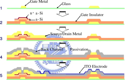
2.1 Process of inverted amorphous thin-film transistor . . . 23
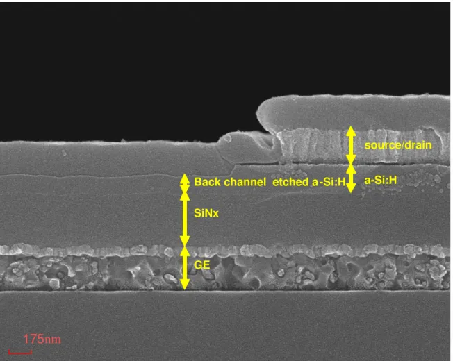
2.2 The SEM image. . . 24
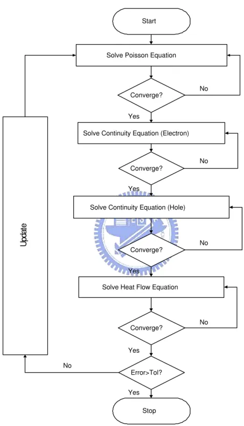
2.3 A flow chart of the Gummel’s decoupling algorithm. . . 42
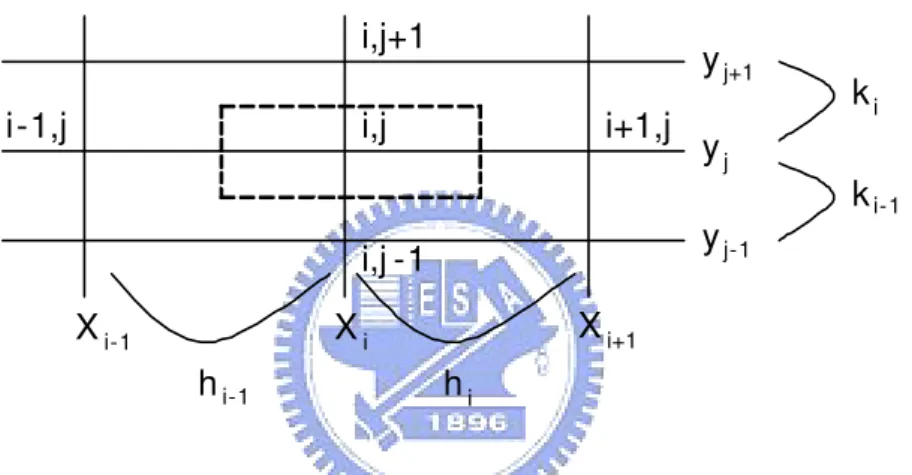
2.4 The example of FVM with example of Poisson equation. . . 43
2.5 The flow char of FVM. . . 44
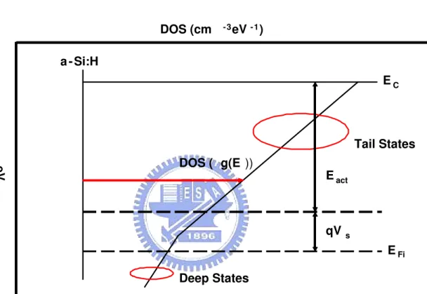
3.1 Eact-EC-EF i-qVS is the activation energy. . . 53
3.2 Schematic representation of the inverted staggered a-Si:H TFT with UV illumination from the top side. . . 55
3.3 (a) Instrument to extraction ID-VG curve with source-drain voltage of 12 V from 0 shot to 101 shots. (b) Instrument to UV illumination with wave-length of 355 nm. . . 56
3.4 Measured drain current versus the gate voltage for the source-drain voltage of 12 V from 0 shot to 101 shots. . . 62
xiv LIST OF FIGURES
3.5 Calculated and measured drain current as a function of gate voltage for the
source-drain voltage of 12 V. . . 63
3.6 Simulated acceptor-liked states of gtcwith different numbers of UV illumi-nation shot. . . 64
3.7 Simulated acceptor-liked states of gdc with different UV illumination. . . . 65
3.8 Model density of states used in a-Si:H with 0 shot. . . 66
3.9 Model density of states used in a-Si:H with 10 shots. . . 67
3.10 Model density of states used in a-Si:H with 22 shots. . . 68
3.11 Model density of states used in a-Si:H with 50 shots. . . 69
3.12 Model density of states used in a-Si:H with 101 shots. . . 70
3.13 Model density of states used in a-Si:H with 0, 22, and 101 shots, respectively. 71 3.14 Activation energy versus the gate voltage for the source-drain voltage of 12 V from 0 shot to 101 shots. . . 72
3.15 (a) Simulated generation rates of the trap-assisted tunneling with 22 shots at VD = 12 V and VG = -20 V. (b) Simulated generation rates of the band-to-band tunneling with 22 shots at VD= 12 V and VG= -20 V. . . 73
LIST OF FIGURES xv 3.16 (a) Simulated maximum generation rates of the trap-assisted tunneling (TAT)
and band-to-band tunneling (BBT) from 0 shot to 101 shots at VD = 12 V
and VG = -20 V. (b) Relation between leakage current and trap density at
1.2 eV which is higher than valence band. . . 74 3.17 Simulated drain current as a function of gate voltage without traps filled for
the source-drain voltage of 12 V. . . 75 3.18 Simulated drain current as a function of time with traps filled for the
Chapter 1
Introduction
I
n this chapter, we introduce the background, consisting of device characteristics and stability mechanism, and motivation. There are more discussions about a-Si TFTs, such as photodegradation, technologies, static characteristics, dynamic characteristics, sta-bility, and so on. Hydrogenated amorphous silicon thin-film transistors (a-Si:H TFTs) haverecently been widely used as switching devices for large-area electronics such as active ma-trix liquid crystal displayers (LCD). Unfortunately, a-Si:H TFT is high photoconductivity and may result in high leakage current under light illumination, especially those projectors
and displays with high intensity backlight illumination. The leakage current thus causes a voltage drop and then induces insufficient rotation angle of liquid crystal. There are some solutions to this problem.
2 Chapter 1 : Introduction
1.1
Background
In this section, we describe the effect of photoillumination on a-Si TFT. The structure of
a-Si TFT may be divided into four types, in which the inverted-staggerd type is the most popular one. The electric characteristics may be influenced by two kinds of trap states. Others such as effects of redistribution, gate insulators and bias-temperature stress on a-Si
TFTs are also discussed in this section.
1.1.1
Device Characteristics
Amorphous silicon thin-film transistors were first proposed for device applications LeComber
in 1979 [1]. Since then, there has been enormous amount of activity, worldwide, that has resulted in the utilization of these devices in a variety of applications. In recent years, the hydrogenated amorphous silicon thin-film transistors (a-Si:H TFTs) have been widely
used as switching devices for large-area electronics such as active matrix liquid crystal displayers, linear arrays of image sensors for facsimile readers [2], and linear arrays for driving new page-width printers [3]. For these applications, one requires a large area,
low-temperature technology compatible with cheap glass substrates. As the TFT turns on, both the liquid crystal capacitance and the associated capacitance are charged, which have to sustain enough voltage for the rotation of liquid crystal. Unfortunately, a-Si:H TFT is high
1.1 : Background 3 photoconductivity and may result in high leakage current under light illumination, espe-cially those projectors and displays with high intensity backlight illumination. The leakage
current thus causes a voltage drop and then induces insufficient rotation angle of liquid crystal. Therefore, when employing an a-Si:H layer, the main objectives are to enhance the field effect mobility and to reduce the off-state leakage current under light illumination.
Mobility has a direct influence on the display performance, particularly in high-resolution displays or sensors. On the other hand, a-Si:H has high photoconductivity which results in high off-state leakage current of a-Si:H TFTs under light illumination [4].
The observation of metastable changes in a-Si:H goes back to the work of Staebler and Wronski [5], who found in 1977 that the dark conductivity and photoconductivity of glow-discharge deposited amorphous silicon can be reduced significantly by prolonged
illumi-nation with intense light (600-900 nm), and can be reversible with low-anneal temperature (=150◦ C). Also, they think that the effect of the optical exposure is to increase the den-sity of gap states. The authors proposed that these effects were due to reversible changes
in the bulk density of states which caused a shift of the Fermi level and, hence changed the dark conductivity. Thereafter, in 1982, Powell, Easton, and Nicholls [6] presented the results of the measurements of the field-effect conductance of amorphous silicon, which
was subjected to the same cycle of annealing and illumination reported by Staebler and Wronski. The cycle of annealing and illumination has two effects: to change the threshold
4 Chapter 1 : Introduction
voltage and to change the off conductance. Moreover, they considered the changes in field-effect conductance due to annealing and illumination that would be expected according to
the bulk [7] and surface models [8]. According to the bulk model, illumination causes a metastable increase in the bulk density of states in the semiconductor. The charge state and energy position of the defect states must be such that they cause the Fermi level to
move away from the conduction band after illumination. And the surface state density is negligible [6]. On the other hand, according to the surface model, it is proposed that there is positive fixed charge density in nitride, leading to an accumulation layer in the
semicon-ductor. Illumination leads to a high density of mobile electrons in the semiconductor, some of which tunnel into traps in the insulator, thereby neutralizing the positive fixed charge and reducing the space-charge region in the semiconductor. And the off conductance would be
determined by a space-charge region at the opposite side of the film, which would not be much affected by the gate electrode. On the other hand, if the surface effect occurred only at the silicon-nitride interface, this would result in only a change in the threshold voltage
and no change in the off conductance [6]. Therefore, the field-effect of a-Si TFTs may be explained by either the density of states in amorphous silicon layer or surface states at both sides of the amorphous silicon layer, i.e. front and rear sides.
1.1 : Background 5 about a-Si TFTs, such as technologies, static characteristics, dynamic characteristics, sta-bility, and so on [9].
Amorphous silicon thin-film transistors can be made with a wide variety of structures and materials. Basically there are four types of planar TFT, i.e. staggered, coplanar, inverted-staggered, and inverted-coplanar types, defined by the order of deposition of the
semiconductor layer, the gate insulator layer, the source-drain contacts, and the gate elec-trode. The staggered TFT structures have the gate source and drain contacts on one side of the semiconductor and the gate electrode on the opposite side, while the coplanar
struc-tures have all three electrodes on the same side of the semiconductor film. In the ”inverted” structures, the gate electrode is the first layer deposited on the glass substrate. For a-Si TFTs, the most popular structure and the one responsible for the state of art performance,
is the inverted-staggered TFT, which uses silicon nitride as the gate insulator [10, 11]. In contrast to poly-Si TFTs, which are usually coplanar, which is the nearest thin-film analog of crystalline Si MOSFET.
The application of a gate voltage leads to an approximately exponential increase in the source-drain current, at first, followed by a linear increase in current at higher gate voltages. Typical threshold voltages are in the range 2-4 V and state of the art
mobili-ties are in the range 0.4-1.0 cm2V−1s−1. Also, for most transistors, the threshold volt-age (given by the intercept of the linear region) and the effective mobility (given by µf e=
6 Chapter 1 : Introduction
(dinsL/εVDW)(dID/dVG), where dID/dVG is the slope of the linear region). The density
of states in amorphous silicon layer can be divided into two types, tail states and deep
states [6]. The tail states are the Si conduction band states broadened and localized by the disorder to form a ”tail” of localized states just below the conduction band mobility edge. These states are so-called the weak silicon bond. The deep states originate from defects in
the a-Si network. These are thought to mostly consist of Si dangling bonds, which have wide range of energies because of the variations in local environments, and this can be im-proved by incorporating hydrogen, forming hydrogenated amorphous silicon (a-Si:H). For
positive gate volts, less than the threshold voltage, the energy bands bend downward and the Fermi level moves through the deep states, which are than occupied. At the same time, some space charge is located in the band-tail states, but the occupancy of these states is
low, since they are well above the Fermi level and so the total space charge is dominated by the deep states. And this leads to approximately exponential increase in the source-drain current. Above the threshold, the space charge in the band-tail states exceeds the space
charge in the deep states, even though the Fermi level is still below the tail states. And this leads to a linear increase in source-drain current.
In most applications, the thin-film transistor acts as a switch, where typically the
transis-tor is switched on for tens of microseconds and then switched off for tens of milliseconds. Shortly after switch on, the deep states begin to trap charge but the rate of trapping is much
1.1 : Background 7 higher near the gate insulator interface, due to much higher density of free carriers, and thermal equilibrium occupancy of the deep states is soon established in that region.
How-ever, trapping of free carriers in the region far from the gate insulator interface continues, leading a transfer of charge from the region near the gate insulator interface to the region far from the gate insulator interface and a change in the band-bending profile, i.e. reducing
the downward band bending [12]. As a result, the redistribution of charge between the tail states and the deep states can be described as an effective dynamic threshold voltage shift, causing the reducing source-drain current [12]. When after switch off, the energy bands are
pushed up and the band-tail electrons are rapidly swept out to the source and drain contacts. After that, electrons begin to emit from the deep states at a rate determined by their energy depth. This continues, building up a uniform space charge in the amorphous silicon, until
the positive space charge in the silicon equalizes the negative charge on the gate. At this point thermal equilibrium is established in the region far from the gate insulator interface, but the deep states in the region near the gate insulator interface continue to emit, leading
to a slow transfer of charge from the region near the gate insulator interface to the region far from the gate insulator interface and again a change in the band-bending profile, i.e. enhancing the upward band bending [12].
8 Chapter 1 : Introduction
Stability influences the lifetime of the device, which is the most important issue. Sub-jecting MOS capacitor and transistors to bias-temperature stress is often used to
inves-tigate the stability of devices, by measuring the resulting threshold voltage shift. The bias-temperature stress applies constant gate voltage and constant temperature annealing for a period of time. When it comes to the stability of a-Si TFTs, two models have been
proposed to account for this threshold voltage shift, namely charge trapping in the silicon nitride gate insulator [13, 14] and the metastable creation of new states in the amorphous silicon [15–17]. If charge is trapped in the nitride under higher positive bias stress (higher
than VGC), then the threshold voltage for both electron and hole conduction shifts to more
positive values [13]. This is because of positive fixed charge in the nitride, leading electron to be trapped. It is interesting that silicon nitride is used in memory devices utilizing this
charge trapping phenomenon. However, the crucial difference with a-Si TFTs is that these devices operate with relatively low fields in the dielectric, by hopping at the Fermi level, but not by direct tunneling from valence band, Fowler-Nordheim injection, trap-assisted
injection, constant energy tunneling from conduction band, or tunneling from conduction band to the Fermi level [13]. Both memory devices trapping and a-Si TFTs hopping occur in the middle of the band gap of nitride [14]. On the other hand, when we apply lower
pos-itive bias stress (lower than VGC), if extra deep states are created in the amorphous silicon
1.1 : Background 9 then the threshold voltage for hole conduction will shift to negative value, while the thresh-old voltage for electron conduction will still shift to a more positive value. There may be
two models to explain the state creation, i.e. local reaction of a silicon-silicon bond with nearby hydrogen (involving breaking a Silicon-Silicon bond) and emission of hydrogen out of a silicon-hydrogen bond (involving long-range hydrogen diffusion) [18]. Moreover,
be-cause the prethreshold slope in the transfer characteristics of n-channel transistors does not change after the bias stress, the newly created states must be located below the flat-band Fermi level. Finally, the threshold shift is independent of temperature for the charge
trap-ping, but is thermally activated for the state creation [19]. The logarithmic time dependence is observed for the charge trapping, but the power law time dependence is observed for the state creation [19].
In order to understand effects of the bias-temperature stress on a-Si TFTs, the defect pool must be first described. In previous statements, both conduction and valence tail states are described as exponential distribution [20]. Thereafter, we continue to describe the defect
in a-Si:H layers. The weak bond state is converted to dangling bond, which is either pos-itively charged or negatively charged, depending on whether the states are created under electron or hole accumulation [21, 22]. In n-type a-Si TFTs, because there are more
elec-trons, the density of states in amorphous silicon layer contains more De states (negatively
10 Chapter 1 : Introduction
(positively charged Si dangling-bond states and located in the upper part of the gap). In p-type a-Si TFTs, because there are more holes, the density of states in amorphous silicon
layer contains more Dh. states than De states. Hence, for the reason of neutral condition,
the Fermi level in n-type devices is at the position close to conduction band edge, while the Fermi level in p-type devices is at the position close to valence band edge. The
equi-librium density of dangling-bond states depends on the Fermi level energy, which leads to a higher density of dangling bonds in doped amorphous silicon than undoped amorphous silicon [23]. We can also make use of a relationship between the subthreshold slopes and
density of states at the Fermi level, which allows comparison of the density of states in the upper part of the gap (related to the electron subthreshold slope) to that in the lower part of the gap (related to the hole subthreshold slope) [24]. Also, the fewer Dh states, the
smaller values of the electron subthreshold slope. The fewer De states, the smaller values
of the hole subthreshold slope. Most current applications of a-Si:H TFTs use them as a simple switches , where we need a high on-off ratio for the lowest possible switching
volt-age. This means good n-channel transistors, with no hole conduction at moderate negative bias. For the lowest prethreshold slope, we require a low density of Dh states and for the
suppression of the hole conduction we require a large density of Destates [21]. Moreover,
the density of states has dependence on the gate insulator of a-Si TFTs [24, 25]. For ex-ample, when employing nitride as gate insulator, more deep states occupy in the lower part
1.1 : Background 11 of amorphous silicon gap. On the contrary, when employing oxide as gate insulator, more deep states occupy in the upper part of amorphous silicon gap. This is because of positive
fixed charge in nitride, inducing an electron accumulation layer in the amorphous silicon, like n-type amorphous silicon, even the amorphous silicon is undoped. In the case of ox-ide, there is negative fixed charge, inducing an electron depletion layer in the amorphous
silicon, like p-type amorphous silicon, even the amorphous silicon is undoped. Therefore, the electron threshold voltage is lower and the subthreshold slope is steeper when we use nitride as gate insulator but not oxide, which is the most suitable switch. Now, effects of the
bias-temperature stress on a-Si TFTs can be perfectly described. The following description does not include the charge trapping in the gate insulators. For transistors made with sili-con oxide as gate dielectric, the threshold voltage shift induced under positive bias stress
is due to the creation of De states. The threshold shift induced by negative bias stress is
due to the creation of Dh states. In transistors made with silicon nitride as gate dielectric,
positive bias stress causes an increase in the density of De states, but negative bias stress
causes mainly a reduction in the density of De states. This is why that when we apply
lower positive bias stress, the threshold voltage for electron conduction will still shift to a more positive value. Positive bias annealing of both oxide and nitride transistors leads to
an increase in the density of Destates and a reduction in the density of Dh states. Negative
12 Chapter 1 : Introduction
of Dhstates. Hence, the nitride TFT could be altered by negative bias annealing to become
more like the oxide TFT and the oxide TFT could be altered by positive bias annealing to
become more like the nitride TFT [25].
The density of states in the mobility gap of a-Si:H has been extensively studied us-ing different experimental techniques such as field-effect measurement [26], transient and
steady-state photoconductivity measurements [27], and deep-level transient-capacitance spectroscopy (DLTS) [28]. In addition, other methods such as capacitance-voltage char-acteristics (C-V) [29], and dependence of capacitance on temperature and frequency in
Schottky diodes and metal-oxide-semiconductor (MOS) structures [30] are also used for study of the density of states in a-Si:H. The localized states in a-Si:H mobility gap may be modeled by exponential distributions of deep and tail states for both acceptor-like and
donor-like states [31–33]. The localized states in the upper half of the mobility gap closer to the conduction band edge behave as acceptor-like states, while the states in the lower part of the gap closer to the valence band edge behave as donor-like states. Acceptor-like
states are neutral when empty and negatively charged when filled with an electron, whereas donor-like states are positively charged when empty and neutral when filled with an elec-tron. The density of states is asymmetrical in a-Si:H, i.e. the number of donor-like states
in the mobility gap is higher than the number of acceptor-like states. As a result, following the neutrality condition, the position of the Fermi level in an intrinsic a-Si:H sample in the
1.1 : Background 13 dark is closer to the conduction band edge.
1.1.2
Stability Mechanism
The degradation kinetics, i.e. the threshold voltage shifts of a-Si:H TFTs during applied
gate bias, have been unified for different times and temperatures by the thermalization-energy concept and modeled by a nonstretched exponential two-parameter fit, as described in the equation (1.1) [34].
∆Vt(Eth) = [Vbias− Vt(0)] × [1 −
1
exp (Eth− Ea)/kT0+ 1
], (1.1)
where the parameter kT0 exhibits a clear correlation to the Urbach energy, the more
im-portant parameter Ea exhibits no simple correlation on the Urbach energy, the hydrogen
content, nor the hydrogen diffusion coefficient, but is believed to depend on the some deposition-induced microstructure of the material, in other words, respective of condition of the deposition [35]. Two main regimes have been identified for the rf PECVD of a-Si:H.
The first is the so-called α regime, in which the growth rate is lower and the partial pressure of SiH4is also lower. On the other hand, the other one is γ regime, in which the growth rate
is higher and the partial pressure of SiH4 is also higher. In addition to above description,
there are more characteristics in both regimes, e.g. mobility, kT0, and Ea [18]. Mobility
has a direct influence on the display performance, particularly in high-resolution displays or sensors. It is observed that the mobility is higher in α regime. From the equation (1.1),
14 Chapter 1 : Introduction
it is found that the most stable TFT corresponds to the maximum of the ratio Ea /kT0,
which corresponds the boundary of the two regimes. Luckily, the mobility still maintains
a high value. In the section 1.1.1, it is referred that there may be two models to explain the state creation by bias stress. In the first model, local reaction of a silicon-silicon bond with nearby hydrogen, for example, Si-Si + SiHHSi→ 2SiHD. SiHD is a singly
hydro-genated Si-Si bond, electrically indistinguishable from an isolated Si dangling bond. This rearrangement will involve the energy to break a silicon-silicon bond, which is known to be exponentially distributed in energy [36]. It is related with the defect creation. In the
second model, emission of hydrogen out of a silicon-hydrogen bond (SiHHSi or H2) to
the hydrogen mobility edge, followed by long-range hydrogen diffusion and final trapping of the hydrogen in a silicon- silicon bond, creating a SiHD defect [37]. The SiHHSi are
exponentially distributed in energy based on the hydrogen density of states model [38]. This reaction path will only involve the Si-H bonding energy. It is related with the defect removal.
1.2
Motivation
Hydrogenated amorphous silicon thin-film transistors (a-Si:H TFTs) have recently been widely used as switching devices for large-area electronics such as active matrix liquid crystal displayers (LCD). As the TFT turns on, both the liquid crystal capacitance and the
1.2 : Motivation 15 associated capacitance are charged, which have to sustain enough voltage for the rotation of liquid crystal. Unfortunately, a-Si:H TFT is high photoconductivity and may result in high
leakage current under light illumination, especially those projectors and displays with high intensity backlight illumination. The leakage current thus causes a voltage drop and then induces insufficient rotation angle of liquid crystal. A well-known popular approach to
re-duction of the leakage current is to reduce the thickness of a-Si:H. However, the prore-duction yield of large size TFT-LCD is decreased . Recently, Fluorine and Chlorine incorporated a-Si:H have been proposed to suppress the off-state leakage current by the shift of the
Fermi level toward the valence band edge due to the increase of acceptor-liked states in a-Si:H (Fluorine) material. Observation of the increase of acceptor-liked states motivates us to explore the reduction mechanism of the off-state leakage current for a-Si:H TFTs.
The influence of prolonged illumination with intense light (wavelength 600-900 nm) on the metastable changes in a-Si:H film was observed. However, seldom attention was drawn on studying the ultraviolet (UV) illumination induced metastable increase in hydrogenated
materials.
Also, for transmissive LCD panel, under environmentally scattering ambient light illu-mination, the UV light influences the devices through black matrix with certain dosage and
probability. The general RPI model is lack of photo-induced phenomenon and mechanism for numerical device simulation. It is, therefore, worth investigating the inside qualitatively
16 Chapter 1 : Introduction
and quantitatively physical mechanism for the device compact model.
1.3
Outline
The thesis is organized as follows. The fabricated process, simulation, and characterization for analyzing the device characteristics are introduced in the chapter 2, where the corre-sponding density and distribution of trap states and the recombination-generation
mecha-nisms consisting of Shockley-Read-Hall recombination and band-to-band tunneling recom-bination are included. In the chapter 3, the variation of I-V characteristics under different UV illumination exposure are for the first time measured and calibrated. The UV
illumina-tion induced electrical and physical characteristic variaillumina-tions are studied. Finally we draw conclusions in the chapter 4.
Chapter 2
Fabrication and Simulation
I
n this chapter, we introduce the fabrication, consisting of properties of some layers in a-Si:H TFT and process flow, simulation models and numerical methods. Physical models contain the two-dimensional thermodynamic model, the mobility model, the trapmodel, and the recombination model. Numerical methods include the Gummel’s decou-pling, adaptive finite volume, and newton’s iterative methods.
2.1
Fabrication
In this section, we discuss some properties of a-Si:H, SiNx, and n+- a-Si:H layers. For
undoped a-Si:H, the deposition temperature is about 220-350◦C, while for SiNx is about
18 Chapter 2 : Fabrication and Simulation
300-350◦C. In addition to temperature, RF power and gas dilution also influence the per-formance of a-Si TFT. Besides, the best material for the TFTs is a N-rich SiNx. The n+
-a-Si:H layers formation are used to allow the formation of an ohmic contact.
2.1.1
Characteristics of a-Si:H, SiN
x, and n
+- a-Si:H layers
The TFT performance depends on the preparation conditions, such as substrate tem-perature, RF power, and gas dilution. Typically, undoped a-Si:H for TFT application
is prepared at a substrate temperature of 220-350◦C. Films of a-Si:H deposited by PECVD at lower RF power have better step coverage and low defect density, whereas a-Si:H films deposited at higher RF power have poor step coverage and high defect density. Moreover,
increasing the RF power decreases the surface diffusion length of precursor radicals and increases the sticking coefficient to the substrate. Hydrogenated amorphous silicon has short-range order, which means that the coordination Si within 2 or 3 atomic distances, but
there is no periodicity in the long range. Because of this there are a considerable number of localized states in the gap. The hydrogen in the a-Si:H reduces the dangling bonds by passivation. Therefore, the dangling bond density of 1020cm−3in vacuum-evaporated a-Si or sputtered a-Si is reduced to 1015∼1016 cm−3 in PECVD a-Si:H, where hydrogen con-tent is 10-30 at◦/◦. The hydrogen reduces the tail-state density in addition to the reduction
2.1 : Fabrication 19 hydrogen in a-Si:H may be incorporated as SiH or SiH2; however, only films with
hydro-gen bonded as Si-H are suitable for TFT application [39]. The role of hydrohydro-gen during
the deposition in the PECVD chamber can be summarized as follows: Hydrogen atoms cover the growing surface and increase the diffusion length of the Si precursors, and the precursor for a-Si:H depositions is SiH3 [40]. Therefore, the precursors can migrate to a
more stable position [41]. Atomic hydrogen diffuses into the silicon network down to a few nanometers and thus enhances the relaxation of Si atoms, leading to the more stable structure [42]. Atomic hydrogen etches the weak Si-Si bonds and thus more stable Si-Si
bonds are formed [43]. Moreover, the hydrogen content decreases with increasing substrate temperature because of the enhanced out-diffusion of hydrogen from the film. Therefore, the optical band gap deceases when increasing the substrate temperature, since the optical
band gap increases with hydrogen content in the a-Si:H [18].
Plasma-deposited silicon nitride, SiNx is used for the passivation film, silicon nitride
protects against the diffusion of water vapor, sodium, and oxygen into the active device.
Silicon nitride has an amorphous structure, and properties depending on the relative atomic concentrations of silicon, nitrogen, and hydrogen. For good-electrical-quality a-Si:H TFTs, PECVD-deposited SiNx is much more suitable than stoichiometric Si3N4. Silicon nitride
deposited at 300-350◦C (abbreviated as SiNx or SiN:H) is quite different material from
20 Chapter 2 : Fabrication and Simulation
is much less than that of a CVD Si3N4. The interface charge density between a-Si:H and
SiNx is typically in the range of 2x10¹¹ to 7x10¹² eV−1cm−2, and it strongly depends on
the deposition conditions: it increases with decreasing substrate temperature or decreasing RF power. Note that the trap density in SiNx increases on heating above 400◦C, because
the hydrogen is out-diffused as a result of breaking of hydrogen bonds in Si-H and /or N-H
modes. The ability to form a good insulating film at low temperature (less than 350◦C) having a low interface state density with a-Si:H (∼1011 eV−1cm−2 makes a good insula-tor., and the best material for the TFTs is a N-rich SiNx [45]. The interface between SiNx
and a-Si:H affects the field-effect mobility; in particular, the surface roughness of the SiNx
layer is important because it affects the initial growth of a-Si:H, which forms the active channel layer for the TFT [46].
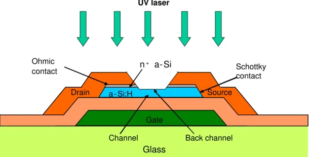
Deposition of an n+- a-Si:H layer between undoped a-Si:H and a metal allows the for-mation of an ohmic contact between them. The ohmic contact also acts to depress the position of the metal. For typical AMLCD TFT channel lengths (∼10 µm) and for
thick-ness of a-Si:H below ∼100 nm, the used of n+ poly-Si or n+ a-Si contact layers dose not appreciably increase the drain current over that of standard n+a-Si:H contact.
2.1 : Fabrication 21
2.1.2
Process Flow
A back-channel-etched (BCE) , inverted-staggered a-Si:H TFTs fabricated on glass
sub-strate was used for electrical measurement. First, the gate electrode of 350 nm thick Mo/AlNd (GE) alloy was deposited by physical vapor deposition method on the glass
sub-strate and was patterned. Thereafter, the 330 nm thick silicon-nitride (SiNx), 110 nm thick
undoped a-Si:H layer, 90 nm thick n+ a-Si:H were successively deposited by chemical va-por deposition method and the a-Si:H layers were patterned. The silicon-nitride layer is
served as the gate insulator. The undoped a-Si:H layer is served as the active layer. The n+ a-Si:H layer is used to form the ohmic contacts at source/drain junction on the top side. The 200 nm thick Mo source/drain electrodes were also deposited by physical vapor deposition
method and were patterned. The n+ a-Si:H layer in the TFT channel region was etched off by dry etching method and was overetched until the undoped a-Si:H layer to avoid the short between source and drain because of high conductivity of n+ a-Si:H layer. The back channel passivation layer (Si3N4) of 200 nm thick was deposited by chemical vapor
depo-sition method and was patterned. Finally, the contact hole was defined and was deposited with 50 nm ITO layer by physical vapor deposition method, as a pixel electrode (connected
with source or drain). All the process is depicted in the figure 2.4. The SEM picture of fab-ricated sample is shown in the figure 2.2. The device is with 18 µm channel width, 5 µm channel length, and 100 nm channel thickness. The electron affinity of the undoped a-Si:H
22 Chapter 2 : Fabrication and Simulation
layer ranges from 3.40 to 4.05 eV and the thickness of nitride is 330 µm with 6.7 dielectric constant and 5.2 eV bandgap. The source/drain contacts on the side walls of the a-Si:H
layer are the schottky contacts because the workfunction of Mo is higher than the electron affinity of the undoped a-Si:H layer. The back-channel-etched (BCE), inverted-staggered a-Si:H TFTs are used as a switch to control the pixel in AMLCD.
2.1 : Fabrication 23 5 5 4 4 3 3 2 2 1 1 5 5 4 4 3 3 2 2 1 1 Gate Metal Gate Insulator a - Si n+ a - Si Source/Drain Metal
Back Channel Passivation
ITO Electrode Glass
24 Chapter 2 : Fabrication and Simulation
GE SiNx
a-Si:H Back channel etched a -Si:H
source/drain
175nm
2.2. DEVICE MODELS 25
2.2
Device Models
In this section, models including thermodynamic, mobility, recombination, and trap mod-els are discussed. The thermodynamic model is consist of four PDEs. The mobility model
contains lattice scattering, ionized impurity scattering, and velocity saturation. The recom-bination model contains both trap-assisted tunneling (by adjustment of lifetime in SRH recombination) and band-to-band tunneling (occurring at high electric fields). The trap
model is implemented by accept-like and donor-like states in a-Si:H layers.
2.2.1
Thermodynamic Model
In this section, we state a 2D steady state mathematical model of TD equations. It is known that classical DD equations consist of three coupled PDEs, the Poisson’s equation, the
current continuity equation of electron, and the current continuity equation of hole [47,48].
∇ε · ∇ψ = −q(p − n + ND+ − NA−), (2.1) ∇ ·−→Jn = qR + q ∂n ∂t, (2.2) −∇ ·−→Jp = qR + q ∂p ∂t, (2.3)
where ψ is the electrostatic potential, ε is the silicon permittivity, q is the elementary charge, n and p are the electron and hole densities respectively, ND+ and NA− are the number
26 Chapter 2 : Fabrication and Simulation
densities respectively, and R is the net electron -hole recombination rate. Both the equations (2.4), (2.2), and (2.3) come from the Maxwell’s equations.
∇ ×−→E = −∂ − → B ∂t , (2.4) ∇ ·−→D = ρ, (2.5) ∇ ×−→H = −−→J + ∂ − → D ∂t , (2.6) ∇ ·−→B = 0, (2.7)
where E and H are the electric and magnetic fields respectively, D and B are the electric and
magnetic flux densities respectively, and ρ and J are the electric charge and total conduc-tion current density respectively. It can be proved that the equaconduc-tion (2.4) comes from the equations (2.4), (2.5) and (2.7), while the equations (2.2) and (2.3) come from the equations
(2.5), (2.6) [49]. Moreover, the electron and hole current densities Jnand Jpare
Jn = −nqµn∇φn, (2.8)
Jp = −pqµp∇φp, (2.9)
where µn and µp are the electron and hole mobilities, and ϕn and ϕp are the electron and
hole quasi-Fermi potentials respectively. It can be proved that both Jn and Jp consist of
carrier diffusion and drift phenomena in semiconductor transport, by Boltzmann Transport Equation on momentum conservation part, and the part to express carrier drift is µ while
2.2. DEVICE MODELS 27 the other is D (defined as diffusion coefficient) [49].
The TD [50] model is defined by the basic set of partial differential equations (2.4),
(2.2), and (2.3), and the lattice heat flow equation (2.10). The relations (2.8) and (2.9) are generalized to include the temperature gradient as a driving term:
c∂T ∂t − ∇ · k∇ · T = −∇ · [(PnT + φn)Jn+ (PpT + φp)Jp] −(EC+ 3 2kBT )∇ · Jp+ (EV − 3 2kBT )∇ · Jp+ qR(EC − EV + 3kBT ), (2.10) Jn = −nqµn(∇φn+ Pn∇T ), (2.11) Jp = −pqµp(∇φp+ PP∇T ), (2.12)
where k is the thermal conductivity, c is the lattice heat capacity, Pnand Pp are the absolute
thermoelectric powers [51], and EC and EV are the conduction and valence band energies,
respectively. In this paper, we use TD model as a fundamental solution to the device simu-lation.
As we know, only PDEs can not be solved to derive the exact solution, there must be
some boundary conditions. There are two main types of boundary conditions, i.e. Dirichlet and Neumann types. Either Dirichlet or Neumann boundary condition on the bounding surface can be obtained by means of Green’s theorem and so-called Green functions [52].
Ohmic contacts are usually described by Dirichlet boundary conditions where potential and carrier concentrations are pre-defined at the contact. Schottky contacts may be mod-eled using Dirichlet conditions which approximate the reverse bias condition or Neumann
28 Chapter 2 : Fabrication and Simulation
boundary conditions based on thermionic emission theory. The absence of current flow through surfaces may be modeled by assuming that the potential and carrier gradients
nor-mal to the surface are zero, which means that the type is Neumann boundary condition [49]. Hence, in the device structure, source/drain (on the top) and gate contacts are fit the type of Dirichlet boundary conditions. The source/drain on the side wall is either Dirichlet or
Neumann boundary condition depending on the bias conditions. The others are fit the type of Neumann boundary condition. For the interface of nitride and a-Si:H, there are no nor-mal components of electron and hole current, so this is Neumann boundary condition.
According to the PDEs and the boundary conditions, this problem can be solved per-fectly.
2.2.2
Mobility Models
In the following sections, we introduce some models used in thermodynamic model, e.g. mobility, recombination, traps model, and so on.
When it comes to the mobility, there are several concepts. First, there are two primary
mechanisms affecting the carrier transport ability, i.e. lattice scattering and ionized impu-rity scattering [53]. Because Si atoms in a semiconductor crystal have a certain amount of thermal energy at temperature above absolute zero that causes the atoms to randomly
2.2. DEVICE MODELS 29 vibrate about their lattice position within the crystal, this phenomenon results in an inter-action between the electrons or holes and the vibrating lattice atoms. This is so-called the
lattice scattering (or phonon scattering), which is dominated in light doped semiconductors. On the other hand, when in heavily doped semiconductors, there may be some coulomb in-teractions between electrons or holes and the ionized impurities, as is the ionized impurity
scattering. Moreover, with the higher field in semiconductors, the carrier drift is no longer proportioned to the electric field strength, instead, the velocity saturates to a finite value vsat [53]. Finally, in the channel region, the high transverse electric field forces carriers to
interact strongly with the semiconductor-insulator interface, meaning the surface scatter-ing [53].
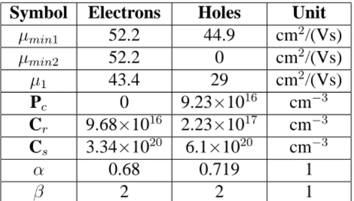
In this work, we employed the following models to describe the mobility.
µdop = µmin1exp(−
Pc Ni ) + µconst− µmin2 1 + (Ni/Cr)α − µ1 1 + (Cs/Ni)β , (2.13)
where the equation (2.13) describes the doping-dependent mobility degradation proposed by Masetti et al. [54]. Moreover, Ni = NA+ ND denotes the total concentration of ionized
impurities, the reference mobilities µmin1, µmin2, and µ1, the reference doping
concentra-tion Pc, Cr, and Cs, and the exponents α and β are accessible in the table 2.1, and the
low-doping reference mobility µconst is 1417 cm2V−1s−1 for electrons and 470.5 cm2V−1s−1
for holes. µac = B F⊥ + C(Ni/N0)λ F⊥1/3(T /T0)k , (2.14)
30 Chapter 2 : Fabrication and Simulation µsr = [ (F⊥/Fref)A ∗ δ + F3 ⊥ η ] −1, (2.15) A∗ = A + α⊥(n + p)Nrefν (Ni+ N1)ν , (2.16) 1 µlow = 1 µdop + D µac + D µsr , (2.17) D = exp(−x/lcrit), (2.18)
where the equations (2.14), (2.15), and (2.16) describe the mobility degradation at interface proposed by Lombardi et al. [55] and Darwish et al. [56], equations (2.17) and (2.18)
describe the Mathiessen’s rule to include both the doping-dependent mobility degradation and the mobility degradation at interface. The surface scattering includes both acoustic surface phonons (µac) and surface roughness (µsr). Moreover, T is the lattice temperature,
T0 = 300 K, the reference field Fref = 1 Vcm−1, F⊥ is the transverse electric field normal
to the semiconductor-insulator interface, D (x is the distance from the interface and lcrit a
fit parameter) is a damping that switches off the inversion layer terms far away from the
interface, n and p denote the electron and hole concentrations, respectively, and Nref = 1
cm−3. All the other parameters are in the table 2.2.
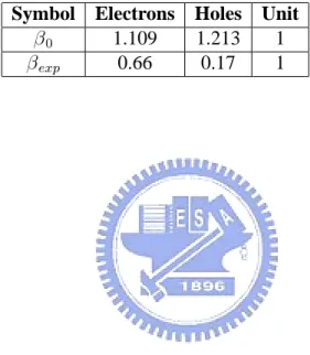
µ(F ) = µlow [1 + (µlowF vsat ) β], (2.19) β = β0(T T0 )βexp, (2.20) vsat = vsat,0( T0 T ) vsat,exp, (2.21)
2.2. DEVICE MODELS 31 where the equation (2.19), (2.20), and (2.21) describe the high field saturation of mobility proposed by Canali et al. [57]. All the parameters are in the tables 2.3 and 2.4.
2.2.3
Recombination Models
The recombination model consisting of Shockley-Read-Hall recombination and band-to-band tunneling recombination is included in continuity and lattice heat flow equations, i.e.
the equations (2.2), (2.3), and (2.10) to describe the characteristic of schottky contact with negative gate bias.
Trap-assisted tunneling [58] (also known as defect-assisted tunneling or field-enhanced
recombination) results in a reduction of SRH recombination lifetimes in regions of strong electric fields. It must not be neglected if the electric field exceeds a value of approximately 3x10⁵ Vcm−1 in certain regions of the device. For example, the I-V characteristics of re-verse biased pn-junctions are extremely sensitive to defect-assisted tunneling, which causes electron-hole pair generation before band-to-band tunneling or avalanche generation sets in. Therefore, it is recommended that this model is included in the simulation of drain
reverse leakage and substrate currents in MOS transistors. The parameter gp(F) is derived
by replacing mΘ,e with mΘ,h and Et with Eg - Et. The upper sign in the equation (2.30)
32 Chapter 2 : Fabrication and Simulation condition of holes. RSRH Et = np − n2 i,ef f τp(n + n1) + τn(p + p1) , (2.22) τp = τmax,p [1 + gp(F )] , (2.23) τn = τmax,n [1 + gn(F )] , (2.24) gn(F ) = [1 + (~Θ)3/2√E t− E0 E0~ω0 ]−1/2 ×(~Θ)3/4(Et− E0)1/4 2√EtE0 ( ~Θ kBT )3/2A(E t, E0, T, εR, ω0, Θ), (2.25) E0 = 2 √ εF[ p εF + Et+ εR− √ εF] − εR, (2.26) εF = 2εRkBT ~Θ , (2.27) εR= S~ω0, (2.28) Θ = ( e2F2 2~mΘ,e )1/3, (2.29) Et = 1 2Eg,ef f ± 3 4kBT ln( mc mv ) ∓ Etrap− (32RC,V~3Θ3)1/4, (2.30) RC = mc( Z2 ε2 )Ry, (2.31)
where E0is the energy of an optimum horizontal transition path, εRis the lattice relaxation
energy, S is the Huang-Rhys factor, ~ω0 is the effective phonon energy, Et is the energy
level of the recombination center, Θ is the electro-optical frequency, mΘ,e is the electron
2.2. DEVICE MODELS 33 electrons and holes respectively, RY is the Rydberg energy, ε is the relative dielectric
con-stant, and Z is a fit parameter.
Phonon-assisted band-to-band tunneling [59] cannot be neglected in steep pn-junctions (with a doping level of 1x1019cm−3or more on both sides) or in high normal electric fields of MOS structures. It must be switched on if the field, in some regions of the device,
ex-ceeds (approximately) 8x10⁵ Vcm−1. The upper sign in the equations (2.32) and (2.34) refers to tunneling generation (np< n2i,ef f) and the lower sign refers to recombination
(np>n2i,ef f).
Rnetbb = AF7/2 enep − n
2
i,ef f
(en + ni,ef f)(ep + ni,ef f)
B(FC, F, ω, T ), (2.32) e n = n(ni,ef f NC )∇EFnF , (2.33) Fc±= B(Eg,ef f ± ~ω)3/2, (2.34)
where ~ω denotes the energy of transverse acoustic phonon.
2.2.4
Trap Models
To include the influence of charge distribution in device characteristics, we have to couple the influence of trap states into our device simulators mentioned above. The influence of trap state is feed in the right hand side of Poisson equation, as shown in below, to study the
34 Chapter 2 : Fabrication and Simulation
effects of trap states in a-Si:H layer.
∇2φ = −q ε[p−n+ND−NA+ X (NDt−nDt)− X (NAt−pAt)+ X pt− X nt], (2.35) nDt = NDtfn, nt= NEtfn, pAt = NAtfp, pt= NHtfp, (2.36) fn= vn thσnn + vthp σpp1 vn thσn(n + n1) + v p thσp(p + p1) , (2.37) fp = 1 − fn, (2.38) vthn,p= v0n,p r T T0 , (2.39)
n1 = ni,ef f exp(Etrap/kBT ), (2.40)
p1 = ni,ef fexp(−Etrap/kBT ), (2.41)
where φ is the electrostatic potential, q is the elementary charge, ε is the semiconductor
permittivity, Etrepresents the energy levels of trap, p is the hole density, n is electron
den-sity, ND is the donor doping concentration, NAis the acceptor doping concentration, NDtis
the donor trap concentration, NAtis the acceptor trap concentration, nDtis the electron
con-centration of the donor trap level, pAtis the hole concentration of the acceptor trap level, pt
is the hole concentration of the neutral hole trap level, ntis the electron concentration of the
neutral electron trap level, NEtis the neutral electron trap concentration, NHtis the neutral
hole trap concentration, fn is the occupation probability for electrons, fp is the occupation
probability for holes, vnth is the electron thermal velocity, vpthis the hole thermal velocity,
2.2. DEVICE MODELS 35 effective intrinsic carrier concentration, and Etrapis the difference between the defect level
and intrinsic level. The trap models used in this study is irrespective of acceptor and donor
types.
X
(NAt− pAt), (2.42)
X
(NDt − nDt), (2.43)
According the previous study [31–33], the localized states in a-Si:H mobility gap can be modeled by the exponential distributions of deep and tail states for both acceptor-like and
donor-like states: NEt= gtcexp( E − EC Etc ) + gdcexp( E − EC Edc ), (2.44) NHt= gtvexp( EV − E Etv ) + gdvexp( EV − E Edv ), (2.45)
where EC is the conduction band edge, gtcand gdc are the densities of states at the
conduc-tion band edge for the tail and deep acceptor-like states, respectively. Etc and Edc are the
associated slope of the exponential distribution of the tail and deep acceptor-like states. EV
is the valence band edge, gtcand gdcare the densities of states at the valence band edge for
the tail and deep donor-like states. Etv and Edv are the associated slope of the exponential
distribution of the tail and deep donor-like states, respectively, and E is the energy in the a-Si:H mobility band gap.
36 Chapter 2 : Fabrication and Simulation
2.3
Simulation Method
In this section, the simulation methods include the Gummel’s decoupling method, the adap-tive finite volume method, and the newton’s iteraadap-tive method. For the purpose of time-consuming, we use the TCAD device simulator to realize the simulation of a-Si TFTs
under different magnitude of UV illumination.
2.3.1
The Gummel’s Decoupling Method
The Gummel’s decoupling method controls an iterative loop over two or more coupled equations. It is used when a fully coupled method would use too many resources of a given machine, or when the problem is not yet solved and a full coupling of the equations would
diverge.
To explore the transport behavior of a-Si TFTs, the three coupled PDEs are numerically solved with Gummel’s decoupling method. With a given initial guess ¡φ(0), n(0), p(0)¢ and for each Gummel’s iteration index g, g = 0,1,. . ., we first solve the nonlinear Poisson equation ∆φ(g+1) = q εs (n(g)− p(g)+ D(x, y) +Xnt− X pt). (2.46)
The nonlinear Poisson equation is solved for φ(g+1)given the previous states n(g) and p(g). The current continuity equation of electron is then solved for n(g+1), with now the known
2.3. SIMULATION METHOD 37 functions φ(g+1), p(g) , and T(g) 1 q∇ · (−qµnn (g+1)∇φ(g+1)+ qD(g+1) n ∇(g+1)n + Pn∇T(g)) = R(n(g+1), p(g)). (2.47)
Thereafter, we solve the current continuity equation of hole with φ(g+1) , n(g+1) , and T(g)known
1
q∇ · (−qµpp
(g+1)∇φ(g+1)+ qD(g+1)
p ∇(g+1)p + Pp∇T(g)) = −R(n(g+1), p(g+1)), (2.48)
Finally, we solve the heat flow equation with φ(g+1), n(g+1), and p(g+1).
c∂T (g+1) ∂t − ∇ · k∇ · T (g+1) = −∇ · [(P nT(g+1)+ φ(g+1)n )Jn+ (PpT(g+1)+ φ(g+1)p )Jp] −(EC + 3 2kBT (g+1))∇ · J p+ (EV − 3 2kBT (g+1))∇ · J p+ qR(EC − EV + 3kBT(g+1)(2.49)), Jn = −qµnn(g+1)∇φ(g+1)+ qDn(g+1)∇(g+1)n + Pn∇T(g+1), (2.50) Jp = −qµpp(g+1)∇φ(g+1)+ qDp(g+1)∇(g+1)p + Pp∇T(g+1), (2.51)
for T(g+1)until all preset stopping criteria are satisfied. The equations (2.46), (2.47), (2.48), and (2.49) are associated with proper boundary condition, respectively. We note that the equations (2.46), (2.47), (2.48), and (2.49) are now four individual semilinear PDEs to be solved for each Gummel’s iteration. An outer iteration in the procedure of a-Si TFT
simulation is then defined by Gummel’s decoupling method.
38 Chapter 2 : Fabrication and Simulation
Begin
While φ, n, p, and T in outer loop (Gummel’s loop) are not convergent If φ is convergent
Solve the nonlinear Poisson equation
with adaptive computing technique. End If
If n is convergent
Solve the current continuity equation of electron with adaptive computing technique.
End If
If p is convergent
Solve the current continuity equation of hole with adaptive computing technique.
End If
If T is convergent
Solve the heat flow equation
with adaptive computing technique. End If
2.3. SIMULATION METHOD 39 Call for next calculation.
EndThe Gummel’s decoupling algorithm
A computational procedure for Gummel’s decoupling method is shown above, and the flow char is shown in the figure 2.3. We solve each decoupled PDE with adaptive computing technique.
2.3.2
The Adaptive Finite Volume Method
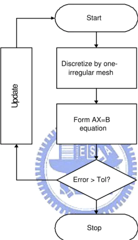
Based on adaptive 1-irregular mesh and finite volume (FV) approximation. The finite
volume method is a numerical method for solving partial differential equations. It calculates the values of the conserved variables across the volume. Before using adaptive finite volume method to solve Poisson equation, we must understand the follow steps:
(1) Weak Formulation transforms into weak problem; (2) Discretize the simulation area by one-irregular mesh; (3) Form the equation “Ax = B” by using FV method; and
(4) Error estimation and mesh refinement.
The example of FVM with Poisson equation is shown in the figure 2.4.
Z Z ∇ · ∇φdydx = Z Z [qni εSi (uexp( φ VT ) − vexp(−φ VT )) −qD εSi ], (2.52)
40 Chapter 2 : Fabrication and Simulation (φi+1,j − φi,j hi )(kj−1+ kj 2 ) + ( φi,j−1− φi,j kj )(hj−1+ hj 2 ) +(φi−1,j − φi,j hi−1 )(kj−1+ kj 2 ) + ( φi,j−1− φi,j kj−1 )(hj−1+ hj 2 ) = [qni εSi (ui,jexp( φi,j VT ) − vi,jexp( −φi,j VT )) − qDi,j εSi ](kj−1+ kj 2 )( hj−1+ hj 2 ), (2.53)
The flow char of FVM is shown in the figure 2.5. The discretized step divides into struc-tured mesh and unstrucstruc-tured mesh. If according to geometry, it divides into rectangle mesh and triangle mesh. But the rectangle mesh is easier to build than the triangle mesh.
2.3.3
The Newton’s Iterative Method
The starting solution of initial guess is determined by using a predetermined algorithm. An initial guess of each variable (at each mesh point) in a device required by the solution
method including electrostatic potential and quasi-Fermi potentials for electrons and holes. To determine an initial guess for the electrostatic potential and quasi-Fermi potentials, the device is subdivided into wells of n- and p-type doping, such that pn-junctions serve as
dividers between wells. Every well is uniquely associated with a contact. The quasi-Fermi potentials in that well are set to the corresponding contact voltage, and the potentials are set to the contact voltage adjusted by the built-in voltage at the contact. For wells that have no
contacts, the following equations define the quasi-Fermi potential for the majority carriers:
2.3. SIMULATION METHOD 41 φn= (1 − kF loat)Vmax+ kF loatVmin, (2.55)
where kF loat is equal to 0. For wells with more than one contact, the well is further
subdi-vided, such that no well is associated with more than one contact.
Newton’s method uses the first and second derivatives when the initial point is closed to the solution. In this sections,first, we will show the full coupled solution. This scheme tries to solve the nonlinear system g(z) = 0 by the Newton method:
− →g + −→g 0−→ x = 0, (2.56) − →zj − −→z j+1= λ−→x , (2.57)
where λ is selected such that kgk+1k < kgkk, but is as close as possible to 1. It handles
the error by computing an error function that can be defined by two methods.The Newton
iterations stop if the convergence criteria are fulfilled. One convergence criterion is the norm of the right-hand side, that is, kgk in the equation 2.51. Natural criterion may be the relative error of the variables measured, such ask(λx)z k.
42 Chapter 2 : Fabrication and Simulation
Start
Solve Poisson Equation
Converge?
Solve Continuity Equation (Electron)
Converge?
Solve Continuity Equation (Hole)
Converge?
Solve Heat Flow Equation
Converge? Error>Tol? Stop U p d a te Yes Yes Yes Yes Yes No No No No No
2.3. SIMULATION METHOD 43 X i-1 Xi Xi+1 yj+1 y j yj-1 i -1,j i+1,j i,j+1 i,j -1 i,j ki ki-1 hi-1 h i
44 Chapter 2 : Fabrication and Simulation Discretize by one-irregular mesh Form AX=B equation Error > Tol? Start Stop U p d a te
2.3. SIMULATION METHOD 45
Table 2.1: Masetti model: Default coefficients.
Symbol Electrons Holes Unit
µmin1 52.2 44.9 cm2/(Vs) µmin2 52.2 0 cm2/(Vs) µ1 43.4 29 cm2/(Vs) Pc 0 9.23×1016 cm−3 Cr 9.68×10¹⁶ 2.23×1017 cm−3 Cs 3.34×10²⁰ 6.1×1020 cm−3 α 0.68 0.719 1 β 2 2 1
Table 2.2: Lombardi model: Default coefficients for silicon.
Symbol Electrons Holes Unit
B 4.75×10⁷ 9.93×106 cm/s C 5.8×10² 2.947×103 cm5/3/(V2/3s) N0 1 1 cm−3 λ 0.125 0.0317 1 k 1 1 1 δ 5.82×10¹⁴ 2.055×1014 cm2/(Vs) A 2 2 1 α⊥ 0 0 cm3 N1 1 1 cm−3 v 1 1 1 η 5.82×1030 2.055×1030 V2/(cms) lcrit 1×10⁻⁶ 1×10⁻⁶ cm
46 Chapter 2 : Fabrication and Simulation
Table 2.3: Canali model parameters (default values for silicon).
Symbol Electrons Holes Unit
β0 1.109 1.213 1
βexp 0.66 0.17 1
Table 2.4: Default velocity saturation parameters (for silicon).
Symbol Electrons Holes Unit vsat,0 1.07×10⁷ 8.37×106 cm/s
Chapter 3
Characterization and Simulation
I
n this chapter, we discuss the effect of backlight, activation energy, and simulation results. Activation energy is used to find the position of the Fermi level. The simulation results include calibration of ID-VGcurve with different magnitude of shot.3.1
Effects of Backlight Illumination
An important application for hydrogenated amorphous silicon thin-film transistors is in switching elements for active-matrix liquid crystal displays. Particularly, a-Si:H TFT is
advantageous to the production of large screen displays and facilitates mass-production. When employing a-Si:H layer, one of the main issues is to improve the production through-put and to reduce the off-state leakage currents under light illumination. In order to reduce
48 CHAPTER 3. CHARACTERIZATION AND SIMULATION
the parasitic capacitance between the gate and source/drain electrodes, a self-aligned a-Si:H TFT structure has been proposed. However, the higher off-state leakage current under light
illumination compared to a conventional TFT has been observed [60]. TFT off-current increases by photoillumination, where a-Si decreases the charge stored on the pixel dur-ing the TFT off-time, and results in gray-scale shaddur-ing, flicker, crosstalk and other display
nonuniformity in the LCD. Because the voltage across the capacitor of liquid crystal has re-lationship with the transmittance and the transmittance has rere-lationship with the gray level, the off-current during holding after finishing charging has an influence on the gray level.
The off-state leakage current of a-Si:H TFT is mainly due to holes induced at the a-Si:H interfaced to a gate insulator. However, under light illumination, electrons are the majority carriers when a negative gate voltage is applied to the TFT because electron mobility is
much higher than that of holes [61]. Much attention has been given to the TFT off-current under illumination from the gate side, because backlight illuminates the TFT from the gate side during TFT-LCD operation. In the case of the inverted a-Si TFT, which is the most
widely employed structure, most of the light is shield by the gate electrode and only the source/drain regions are illuminated from the gate-side illumination [62].
There are some solutions for reducing photo leakage current. The off-state leakage current
can be lowered by reducing the thickness of undoped a-Si:H, however, this also decreases the field effect mobility of the TFT [63]. This is because the transmittance for thin a-Si:H