行政院國家科學委員會專題研究計畫 成果報告
可應用於分析每一層均為非線性的多層與多分枝光波導理
論與多通道分波多工器及全光式開關之研究
研究成果報告(精簡版)
計 畫 類 別 : 個別型 計 畫 編 號 : NSC 96-2221-E-151-025- 執 行 期 間 : 96 年 08 月 01 日至 97 年 07 月 31 日 執 行 單 位 : 國立高雄應用科技大學電子工程系 計 畫 主 持 人 : 吳曜東 計畫參與人員: 碩士班研究生-兼任助理人員:徐瑞鴻 碩士班研究生-兼任助理人員:張仁昌 碩士班研究生-兼任助理人員:邱正紘 碩士班研究生-兼任助理人員:李瑋倫 博士班研究生-兼任助理人員:李建樟 處 理 方 式 : 本計畫涉及專利或其他智慧財產權,2 年後可公開查詢中 華 民 國 97 年 09 月 15 日
可應用於分析每一層均為非線性的多層與多分枝光波導理論與多通道分波多工 器及全光式開關之研究(I)
The study of the theory for analyzing multilayer and multibranch optical waveguides with all nonlinear films and all-optical nonlinear optical waveguide devices(I)
Abstract:
We propose a general method for analyzing a multilayer optical waveguide with all nonlinear layers. This method can also be used to analyze a multibranch optical waveguide structure with all nonlinear layers. The analytical and numerical results show excellent agreement.
中文摘要
我們提出一個分析全域非線性之多層光波導結構的新方法,此方法亦可用來 分析非線性多分支光波導結構。數值分析的結果證明我們的分析是正確的。
Key words: multilayer waveguide; multibranch waveguide; kerr effect.
1. INTRODUCTION
The nonlinear optical waveguide device is a potential key component in the applications of optical signal processing and communication systems [1-3]. In the past, a number of papers have dealt with the propagation characteristics of TE-polarized waves guided by a three-layer lossless linear, or nonlinear optical waveguide structures [4-19]. Considerable progress has been made by considering only Kerr nonlinearities due to the third-order nonlinearity [20]. Most of the interest has been focused on optical waves guided by a single planar waveguide with linear film bounded by nonlinear medium [4-9] or nonlinear film bounded by linear medium [10-15]. Stegeman et al. [7-8] presented a large number of calculations for three-layer optical planar waveguide and provided many rigorous curves of dispersion relation. Boardman et al. [10-11] have well defined the behavior of TE nonlinear waves in an optically nonlinear film by using the Jacobi elliptic function and boundary field approach. Most studies for optical waveguide with nonlinear guiding film are
reviewed by this model. Okafuji [15] expressed for the TE0 waves supported by a
three-layer nonlinear waveguide with a self-focusing nonlinear substrate and a self-defocusing nonlinear film. Sammut et al. [16-17] developed the propagating character in uniform nonlinear medium throughout the cladding, substrate, and guided film. Schürmann [18] used Weierstrass’ elliptic functions to express the field
equations in a nonlinear three-layer structure. Shin et al. [21] presented the five-layer optical waveguide with nonlinear cladding and substrate. Sakakibara [22] and Jeong [23] calculated the field profiles and dispersion relations of nonlinear wave in a slab waveguide with two nonlinear films, respectively. The interests in multilayer optical waveguides, which has been growing steadily in recent years, stem from their potential use for ultra-fast all-optical signal processing and optical computing systems. The analysis of TE wave propagating in the multilayer systems has attracted most attention. Radic et al. [24-26] had proceeded serial rigorous studies in nonuniform distributed feedback structures and presented a general transfer matrix method to analyze the optical wave propagating in this structure. Trutschel et al. [27] developed nonlinear matrix formalism and calculated the field profiles and the propagation constant of the nonlinear guide wave in a multilayer system. Ogusu [28] presented a semi-analytical method for calculated the dispersion relations for stationary nonlinear TE waves guided by general multilayer waveguides with Kerr-like permittivity. She et al. [29] analyzed the nonlinear TE waves in a periodic refractive index waveguide with nonlinear cladding, both by exact method and by the method of root mean square approximation. Wu et al. had developed accurate calculations for multilayer systems, as analyzing the multilayer linear planar waveguide [30], multilayer planar waveguide with nonlinear cladding and substrate [31], multilayer planar waveguide with a localized arbitrary nonlinear guiding film [32], and multilayer planar waveguide with all nonlinear guiding film [33].
The analytical formulas of multilayer systems have potential applications in integrated optics. The multiple quantum well waveguide (MQW) structures can be approximated as a sort of multilayer waveguide [28, 31]. The nonlinear graded-index waveguides can be segmented a number of step refractive index layers [31, 34]. These analyses have also been applied to design the multibranch optical waveguide which can be operated as switches [35], logic gates [36], and wavelength auto-router [37]. In this paper, we propose a general method for analyzing the multilayer optical waveguide structure with all nonlinear layers. The general method can also be degenerated into other special cases for analyzing multilayer nonlinear optical waveguide. This method can be used to predict the propagation characteristics in three-layers, seven-layers, or more. It is useful to design all-optical devices. The dispersion relation curves and electric field profiles for multilayer optical waveguides with all nonlinear layers can be described and compared with the finite difference beam propagation method (FD-BPM) [38]. The analytical and numerical results show excellent agreement.
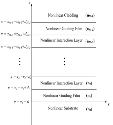
In this section, we use the modal theory [39-40] to derive the general formulas that can be used to analyze the multilayer optical waveguide with all nonlinear layers, as shown in Fig. 1. The multilayer optical waveguide structure is composed of the
guiding films ( 1
2
M − layers), the interaction layers ( 3
2
M− layers), the cladding
layer, and the substrate layer. The total number of layers is M (M=3,5,7,…). The di
and ni are used to denote the width and the refractive index of the i-th layer,
respectively. The cladding and substrate layers are assumed to extend to infinity in the
+x and -x directions, respectively. The major significance of this assumption is that
there are no reflections in the x direction to be concerned with, expect for those occurring at interfaces.
For the simplicity, we consider the transverse electric polarized waves propagating along the z direction. The wave equation in the i-th layer can be written as 2 2 2 2 2 , yi i yi n c t ψ ψ ∂ ∇ = ∂ i=0,1,2,....,M− (1) 1
with solutions of the form
(
, ,)
( )
exp(
e 0)
, 1 yi x z t E xi j t n k z xi x xi ψ ⎡ ω ⎤ + ⎢ ⎥ ⎣ ⎦ = − ≤ ≤ (2)where k0 is the wave number in the free space, and ne is the effective refractive index,
0
c k
ω= . For analyzing conveniently, we choose only self-focusing nonlinear
medium in following discussions. Similar processes can be applied to the intensity-dependent refractive index with self-defocusing nonlinear medium. For the Kerr-type nonlinear medium [20], the square of the refractive index of each layer can be expressed as
( )
2 2 2 0 , 0,1,2,.... 1 i i i i n =n +α E x i= M − (3)where n and i0 αi are the linear refractive index and the nonlinear coefficient of the
i-th layer, respectively. The nonlinear wave equation can be reduced to
( )
( )
( )
2 2 2 3 0 2 0, 0,1,2,.... 1 i i i i i d E x Q E x k E x i M dx − + α = = − (4)where Qi2=k02
(
ne2−ni02)
. The first integration of Eq. (4) gives( )
2 2 2( )
2 4( )
0 1 2 i i i i i i dE x Q E x k E x C dx α ⎡ ⎤ ⎢ ⎥ ⎢ ⎥ ⎣ ⎦ − + = (5)where the first constant of integration Ci can be expressed as
( )
2 2 2( )
2 4( )
0 1 2 i i i i i i i i i x x dE x C Q E x k E x dx α = ⎡ ⎤ ⎢ ⎥ ⎢ ⎥ ⎣ ⎦ = − + (6)For the case Ci≥ , the Eq. (5) can be rewritten as 0
( )
2 2( )
2 4( )
0 1 2 i i i i i i dE x C Q E x k E x dx = ± + − α (7)Integrating Eq. (7), we obtain
(
)(
)
( )
( ) 2 12 0 1 0 2 2 2 2 0 1 , 2 i i i i E x x x x i i i E i i du k dx x x x a u b u α − − + ⎛ ⎞ ⎜ ⎟ ⎝ ⎠ = ± ≤ ≤ + −∫
∫
(8) where 2 2 2 2 0 i i i i q Q a k α − = (9a) 2 2 2 2 0 i i i i q Q b k α + = (9b)(
4 2)
14 0 2 i i i i q = Q + C k α (9c)The transverse electric field in each layer can be written as
( )
{
(
)
}
, 1i i i i oci i i i
E x =b cn q ⎡⎣⎢ x x− +x ⎤⎥⎦m x ≤ ≤x x+ (10)
where cn is one of Jacobi elliptic function, xoci is the second constant of integration, mi
is the Jacobi modulus which can be expressed as
2 2 2 2 i i i i q Q m q + = (11)
Following the approach described in Ref. [10], the transverse electric field in each layer can be rewritten as
(
)
(
)
{
2(
(
)
)
2}
( )
1
1
i i i i i i i i i i i i i i i i i i i i i i icn q x x
B m
E x
A
cn B m
fn q x x m fn B m
Acn q x x m
m sn q x x m sn B m
⎡ ⎤ ⎣ ⎦ ⎡ ⎤ ⎣ ⎦ ⎡ ⎤ ⎡ ⎤ ⎣ ⎦ ⎣ ⎦ ⎡ ⎤ ⎣ ⎦ ⎡ ⎤ ⎡ ⎤ ⎣ ⎦ ⎣ ⎦−
+
=
−
−
=
−
−
−
(12)where Ai is the value of the electric field at the lower boundary in each layer, the
are the Jacobi elliptic functions. sn B m⎡⎣ i i⎤⎦ and fn B m⎡⎣ i i⎤⎦ can be given at the lower boundary x=xi, i i i i i i i i sn B m dn B m fn B m cn B m ⎡ ⎤ ⎡ ⎤ ⎣ ⎦ ⎣ ⎦ ⎡ ⎤ ⎣ ⎦ ⎡ ⎤ ⎣ ⎦ = (13a) i i i i A cn B m b ⎡ ⎤ ⎣ ⎦= (13b)
By matching the boundary conditions, the dispersion equation can be expressed as
1 1 0 1 0 0 fn B m q q fn B m ⎡ ⎤ ⎣ ⎦ = − ⎡ ⎤ ⎣ ⎦ (14a) 1 1 1 1 1 , 2 1 i i i i i i i i fn B m q i M q fn q d B m − − − − − ⎡ ⎤ ⎣ ⎦ = ≤ ≤ − ⎡ + ⎤ ⎣ ⎦ (14b) where i i i i i i i i i i i i sn q d m dn q d m fn q d m cn q d m ⎡ ⎤ ⎡ ⎤ ⎣ ⎦ ⎣ ⎦ ⎡ ⎤ = ⎣ ⎦ ⎡ ⎤ ⎣ ⎦ (14c)
{
}
{
} {
}
2 2 2 2 2 2 2 1 1 i i i i i i i i i i i i i i i i i i i i i i i i i i i i i i i i i i i i i i i i i i i i i i sn q d B m dn q d B m fn q d B m cn q d B m fn q d m dn B m m sn B m cn q d m fn q d m fn B m m sn q d m sn B m fn B m dn q d m m sn q d ⎡ + ⎤ ⎡ + ⎤ ⎣ ⎦ ⎣ ⎦ ⎡ + ⎤ = ⎣ ⎦ ⎡ + ⎤ ⎣ ⎦ ⎡ ⎤ ⎡ ⎤ − ⎡ ⎤ ⎡ ⎤ ⎣ ⎦ ⎣ ⎦ ⎣ ⎦ ⎣ ⎦ = − ⎡⎣ ⎤ ⋅⎦ ⎡⎣ ⎤ ⋅ −⎦ ⎡⎣ ⎤⎦ ⎣⎡ ⎤⎦ ⎡ ⎤ ⎡ ⎤ − ⎣ ⎦ ⎣ ⎦ +{
}
{
} {
}
2 2 2 1 1 i i i i i i i i i i i i i i m cn B m fn q d m fn B m m sn q d m sn B m ⎡ ⎤ ⎡ ⎤ ⎣ ⎦ ⎣ ⎦ − ⎡⎣ ⎤ ⋅⎦ ⎡⎣ ⎤ ⋅ −⎦ ⎡⎣ ⎤⎦ ⎣⎡ ⎤⎦ (14d)Eq. (6) can be rewritten as
(
)
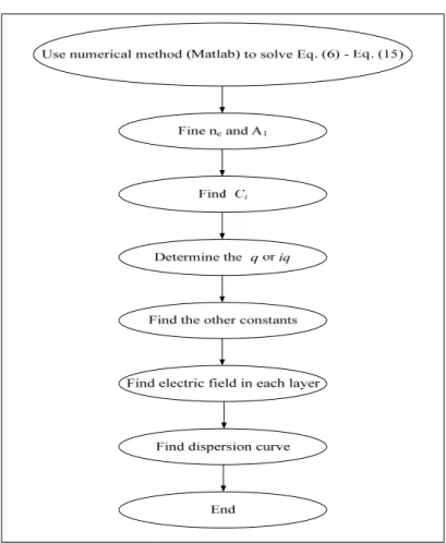
2 2 2 2 2 0 1 2 i i i i i i i i i i C =A ⎧⎨⎣⎡q fn q d +B m ⎤⎦ −Q + k α A ⎫⎬ ⎩ ⎭ (15)The Eqs. (12) to (15) can be solved by a numerical method on a computer. A
diagram indicating the computation step is shown in Fig. 2. When the constants ne and
A1 are determined, all the other constants Qi, Ci, a , i b , i q , i m , and Ai i, are also
determined. For the case Ci ≤ , on the other hand, the transverse electric field and 0
all the other parameters ai, b , i qi , and mi can be expressed as follows:
( )
{
(
)
}
, 1i i i i oci i i i
2 2 2 2 0 i i i i q Q a k α − = (17a) 2 2 2 2 0 i i i i q Q b k α + = (17b)
(
)
1 4 2 4 0 2 i i i i i q =i Q + C k α =iq (17c) 2 2 2 2 i i i i q Q m q + = (17d)We just have to replace the parameters a , i b , i q , and i m in Eqs. (12)-(15) with i
i
a , b , i qi, and mi , respectively, and get these equations with similar expressions.
When the constants ne and A1 are determined, all the other constants Qi, Ci, ai, bi , qi, mi ,
and Ai are also determined.
3. NUMERICAL RESULTS
In this section, we use the analytic formulas derived in the preceding section to calculate the transverse electric field function in each layer of the multilayer optical waveguide structure with all nonlinear layers. We can simplify the general formulas to analyze seven-layer optical waveguides with all nonlinear layers. The numerical
results are shown in Figs. 3(a) and (b). Figure 3(a) shows the dispersion curves of TE0
symmetric modes with the constants n0 = n2 = n4 = n6 = 1.55, n1 = n3 = n5 = 1.57,
2 2
5
0 1 2 3 4 6 6.3786 m V/
α =α α= =α =α =α =α = μ , the free space wavelength λ =
1.55 μm, the width of guiding film d1=d3=d5=2μm, the width of interaction layer d2 =
d4 = 3μm. Figure 3(b) shows the electric field distributions for the various input
powers with respect to points A-D as shown in Fig. 3(a). As the power of film
increases and consequently ne increases, the field distributions gradually narrow, and
the optical wave will be tightly confined in the center nonlinear film.
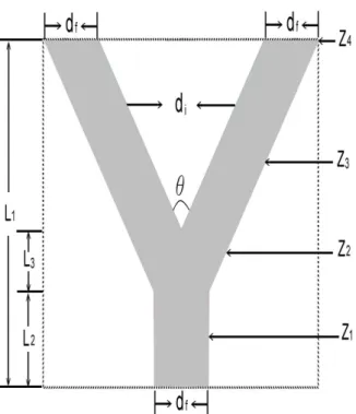
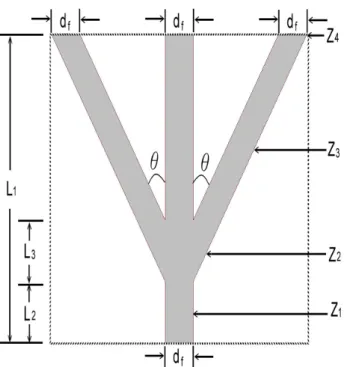
We can also use these general equations to analyze a multibranch waveguide with all nonlinear layers, as shown in Fig. 4. The multibranch waveguides are the key component in the applications of integrated optics. The two-branch waveguide structures can be used in the Mach-Zehnder structures [41] and X junction structures [42]. The three-branch or multibranch waveguide structures can be used in the all-optical switches [35] or power divider [43]. A typical application which combined
two-branch with three-branch had been studied in Ref. [3]. Such the structures also prove a good guide for all-optical devices. In the following analysis the multibranch waveguide is divided into four sections from bottom to top: the straight-line section (three-layer waveguide), the tapered section (three-layer tapered waveguide), the coupled separating-waveguide section (multilayer waveguides with tapered interaction layers), and the isolated separating-waveguide section (multilayer waveguides isolated from one another). The tapered-waveguide section and the separating-waveguide section can be approximated by straight waveguide segments step by step [39-40]. These step-waveguide segments can be analyzed by the method proposed in the preceding section. First, we display an example of a two-branch waveguide structure with all nonlinear layers, as shown in Fig. 5. The parameters of
material are nc0=ns0=ni0=1.55, nf0=1.57, αf =6.3786μm V2/ 2, αc =αs =2αf , the
free space wavelength λ=1.55μm. We discuss the low input power density and the
high input power density cases, respectively.
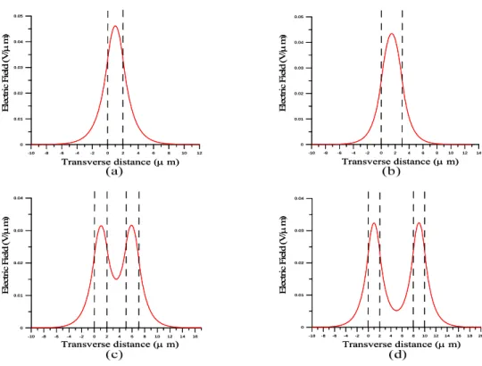
For the low input power density case, the electric field distributions of the four
sections (positions Z1, Z2, Z3, Z4 in Fig. 5) are shown in Figs. 6(a)-(d), respectively. In
Fig. 6(a) the electric field distribution of the straight waveguide section is plotted with
the parameters df=2μm, ne=1.5625. In Fig. 6(b) the electric field distribution of the
tapered-waveguide section is plotted with the parameters df=3μm, ne=1.5655. In Fig.
6(c) the electric field distribution of the coupled separating-waveguide section is
plotted with the parameters df=2μm, di=3μm, ne=1.5615. In Fig. 6(d) the electric field
distribution of the isolated separating-waveguide section is plotted with the
parameters df=2μm, di=6μm, ne=1.5609.
For the high input power density case, the electric field distributions of the four
sections (positions Z1, Z2, Z3, Z4 in Fig. 5) are shown in Figs. 7(a)-(d), respectively. In
Fig. 7(a) the electric field distribution of the straight waveguide section is plotted with
the parameters df=2μm, ne=1.5799 . In Fig. 7(b) the electric field distribution of the
tapered-waveguide section is plotted with the parameters df=3μm, ne=1.5808 . In Fig.
7(c) the electric field distribution of the coupled separating-waveguide section is
plotted with the parameters df=2μm, di=3μm, ne=1.5854 . In Fig. 7(d) the electric field
distribution of the isolated separating-waveguide section is plotted with the
parameters df=2μm, di=6μm, ne=1.5865.
Here we show an example of a three-branch waveguide structure with uniform
nonlinearity, as shown in Fig. 8. The parameters of material are nc0=ns0=ni0=1.55,
nf0=1.57, αc=αs =αf =6.3786μm V2/ 2, the free space wavelength λ=1.55μm. We
respectively. For the low input power density case, the electric field distributions of
the four sections (positions Z1, Z2, Z3, Z4 in Fig. 8) are shown in Figs. 9(a)-(d),
respectively. In Fig. 9(a) the electric field distribution of the straight waveguide
section is plotted with the parameters df=2μm, ne=1.5594. In Fig. 9(b) the electric
field distribution of the tapered-waveguide section is plotted with the parameters
df=4μm, ne=1.5649. In Fig. 9(c) the electric field distribution of the coupled
separating-waveguide section is plotted with the parameters df=2μm, di=3μm,
ne=1.5602. In Fig. 9(d) the electric field distribution of the isolated
separating-waveguide section is plotted with the parameters df=2μm, di=6μm,
ne=1.5594.
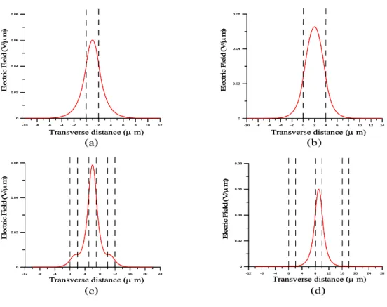
For the high input power density case, the electric field distributions of the four
sections (positions Z1, Z2, Z3, Z4 in Fig. 8) are shown in Figs. 10(a)-(d), respectively.
In Fig. 10(a) the electric field distribution of the straight waveguide section is plotted
with the parameters df=2μm, ne=1.5641. In Fig. 10(b) the electric field distribution of
the tapered-waveguide section is plotted with the parameters df=4μm, ne=1.5688. In
Fig. 10(c) the electric field distribution of the coupled separating-waveguide section is
plotted with the parameters df=2μm, di=3μm, ne=1.5642. In Fig. 10(d) the electric
field distribution of the isolated separating-waveguide section is plotted with the
parameters df=2μm, di=6μm, ne=1.5641.
To prove the accuracy of numerical results shown in Figs. 6-10, we use the FD-BPM [38] to simulate the electric field propagating along these structures with all nonlinear layers, from the stem to the branching waveguides. For calculating the two-branch waveguide structure with all nonlinear layers, we choose the following
numerical data: the transverse step lengthx=0.03125μm, the longitudinal step
length 0.05z= μm, the total propagation distance Z=1100μm, branching angle
θ=0.573°. The simulation results for the low input power density and high input
power density cases are shown in Figs. 11 and 12. The relevant curves shown in Figs. 6-7 and Figs. 11-12 are superposed on the same graph as shown in Figs. 13-14. For calculating the three-branch waveguide structure with uniform nonlinearity, we
choose the following numerical data: the transverse step length x=0.03125μm, the
longitudinal step length z=0.05μm, the total propagation distance Z=1500μm,
branching angle θ=0.382°. The simulation results for the low input power density and
high input power density cases are shown in Figs. 15 and 16. The relevant curves have been shown in Figs. 9-10 and Figs. 15-16 are superposed on the same graph shown in Figs. 17-18. By comparing the results, we confirm that our analyses are correct.
4. CONCLUSIONS
waveguide structure with all nonlinear layers. This model can be degenerated into some kinds of special cases. In the future, the multilayer and multibranch waveguide structures are important key components in application of integrated optics. The multilayer structures have been extensively used in the MQW waveguides and the multibranch structures have also been designed to operate as all-optical devices. This method can be used to predict the evolution of waves propagating along the multibranch optical waveguide structures. Similar processes can be extensively used to predict the propagation characteristics of spatial solitons [37, 44]. We give a detail modal analysis of the proposed nonlinear optical waveguide structure. The analytical and numerical results show excellent agreement.
5. REFERENCES
1. K. Yamada, H. Fukuda, T. Tsuchizawa, T. Watanabe, T. Shoji, and S. Itabashi, “All-optical efficient wavelength conversion using silicon photonic wire waveguide,” IEEE Photonics Technol. Lett. 18, 1046-1048 (2006).
2. Y. D. Wu, “New all-optical switch based on the spatial soliton repulsion,” Opt. Express 14, 4005-4012 (2006).
3. Y. D. Wu, “All-optical logic gates by using multibranch waveguide structure with localized optical nonlinearity,” IEEE J. Sel. Top. Quantum Electron. 11, 307-312 (2005).
4. Jian-Guo Ma and Ingo Wolff, “Propagation characteristics of TE-wave guided by thin films bounded by nonlinear media,” IEEE Trans. Microw. Theory Tech. 43, 790-795 (1995).
5. T. Rozzi, “Modal analysis of nonlinear propagation in dielectric slab waveguide,” J. Lightwave Technol. 14, 229-234 (1996).
6. R. W. Micallef, Y. S. Kivshar, J. D. Love, D. Burak, and R. Binder, “Generation of spatial solitons using non-linear guided modes,” Opt. Quantum Electron. 30, 751-770 (1998).
7. C. T. Seaton, J. D. Valera, R. L. Shoemaker, G. I. Stegeman, J. T. Chilwell, and S. D. Smith, “Calculations of nonlinear TE waves guided by thin dielectric films bounded by nonlinear media,” IEEE J. Quantum Electron. 21, 774-783 (1985). 8. G. I. Stegeman, C. T. Seaton, J. Chilwell, and S. D. Smith, “Nonlinear waves
guided by thin films,” Appl. Phys. Lett. 44, 830-832 (1984).
9. J. G. Ma and I. Wolff, “TE wave properties of slab dielectric guide bounded by nonlinear non-Kerr-like media,” IEEE Trans. Microw. Theory Tech. 44, 730-738 (1996).
Quantum Electron. 22, 319-324 (1986).
11. A. D. Boardman and P. Egan, “S-polarized waves in a thin dielectric film asymmetrically bounded by optically nonlinear media,” IEEE J. Quantum Electron. 21, 1701-1713 (1985).
12. S. W. Kang, “Optical slab waveguides of Kerr material with linear profile,” Opt. Commun. 174, 127-131 (2000).
13. W. Chen and A. A. Maradudin, “S-polarized guided and surface electromagnetic waves supported by a nonlinear dielectric film,” J. Opt. Soc. Am. B 5, 529-538 (1988).
14. Y. F. Li and K. Iizuka, “Unified nonlinear waveguide dispersion equation without spurious roots,” IEEE J. Quantum Electron. 31, 791-794 (1995).
15. S. Okafuji, “Propagation characteristics of TE0 waves in three-layer optical waveguides with self focusing and self defocusing nonlinear layers,” IEEE Proceedings-J 140, 127-136 (1993).
16. R. A. Sammut, C. Pask, and Q. Y. Li, “Theoretical study of spatial solitons in planar waveguides,” J. Opt. Soc. Am. B 10, 485-491 (1993).
17. K. S. Chiang and R. A. Sammut, “Effective-index method for spatial solitons in planar waveguides with Kerr-type nonlinearity,” J. Opt. Soc. Am. B 10, 704-708 (1993).
18. H. W. Schürmann,” On the theory of TE-polarized waves guided by a nonlinear three-layer structure,” Z. Phys. B 97, 515-522 (1995).
19. T. T. Shi and S. Chi, “Nonlinear TE-wave propagation in a symmetric, converging, single-mode Y-junction waveguide,” J. Opt. Soc. Am. B 9, 1338-1340 (1992).
20. G. I. Stegeman, E. M. Wright, N. Finalyson, R. Zanoni, and C. T. Seaton, “Third order nonlinear integrated optics,” J. Lightwave Technol. 6, 953-970 (1988). 21. S. Y. Shin, E. M. Wright, and G. I. Stegeman, “Nonlinear TE waves of coupled
waveguides bounded by nonlinear media,” J. Lightwave Technol. 6, 977-983 (1988).
22. T. Sakakibara and N. Okamoto, “Nonlinear TE waves in a dielectric slab waveguide with two optically nonlinear layers,” IEEE J. Quantum Electron. 23, 2084-2088 (1987).
23. J. S. Jeong, C. H. Kwak, and E. H. Lee, “Optical properties of TE nonlinear waves in planar waveguides with two nonlinear bounding layers,” Opt. Commun.
116, 351-357 (1995).
24. S. Radic, N. George, and G. P. Agrawal, “Optical switching in λ/4-shifted nonlinear periodic structures,” Opt. Lett. 19, 1789-1791 (1994).
switching in nonlinear phase-shifted periodic structures,” J. Opt. Soc. Am. B 12, 671-680 (1995).
26. S. Radic, N. George, and G. P. Agrawal, “Analysis of nonuniform nonlinear distributed feedback structures: generalized transfer matrix method,” IEEE J. Quantum Electron. 31, 1326-1336 (1995).
27. U. Ttrutschel, F. Lederer, and M. Golz, “Nonlinear guided waves in multilayer systems,” IEEE J. Quantum Electron. 25, 194-200 (1989).
28. K. Ogusu, “Analysis of nonlinear multilayer waveguides with Kerr-like permittivities,” Opt. Quantum Electron. 21, 109-116 (1989).
29. S. She and S. Zhang, “Analysis of nonlinear TE waves in a periodic refractive index waveguide with nonlinear caldding,” Opt. Commun. 161, 141-148 (1999). 30. M. H. Chen and Y. D. Wu, “A general method for analyzing the multi-layer
planar waveguide,” Fiber Integrated Opt. 11, 159-176 (1992).
31. Y. D. Wu, M. H. Chen, and H. J. Tasi, “Analyzing multilayer optical waveguides with nonlinear cladding and substrates,” J. Opt. Soc. Am. B 19, 1737-1745 (2002).
32. Y. D. Wu, “Analyzing multilayer optical waveguides with a localized arbitrary nonlinear guiding film,” IEEE J. Quantum Electron. 40, 529-540 (2004). 33. Y. D. Wu and M. H. Chen, “Method for analyzing multilayer nonlinear optical
waveguide,” Opt. Express 13, 7982-7995 (2005).
34. N. Saiga, “Calculation of TE modes in graded-index nonlinear optical waveguides with arbitrary profile of refractive index,” J. Opt. Soc. Am. B 8, 88-94 (1991).
35. Y. D. Wu, “Nonlinear all-optical switching device by using the spatial soliton collision,” Fiber Integrated Opt. 23, 387-404 (2004).
36. Y. D. Wu, “Coupled-soliton all-optical logic device with two parallel tapered waveguides,” Fiber Integrated Opt. 23, 405-414 (2004).
37. Y. D. Wu, “New all-optical wavelength auto-router based on spatial solitons,” Opt. Express 12, 4172-4177 (2004).
38. W. Huang, C. Xu, S. T. Chu, and S. K. Chaudhuri, “The finite-difference vector beam propagation method: analysis and assessment,” J. Lightwave Technol. 10, 295-305 (1992).
39. W. K. Burns and A F. Milton, “Mode conversion in planar-dielectric separating waveguides,” IEEE J. Quantum Electron. 11, 32-39 (1975).
40. M. Izutsu, Y. Nakai, and T. Sueta, “Operation mechanism of the single-mode optical-waveguide Y junction,” Opt. Lett. 7, 136-138 (1982).
41. M. O. Twati, T.J.F Pavlasek, “A three-wavelength Mach-Zehnder optical demultiplexer by on step ion-exchange in glass,” Opt. Commun. 206, 327-332
(2002).
42. H. Yokota, K. Kimura, and S. Kurazono, “Numerical analysis of an optical X coupler with a nonlinear dieletric region,” IEICE Trans. Electron. E78-C, 61–66 (1995).
43. Y. S. Yong, A. L. Low, S. F. Chien, A. H. You, H. Y. Wong, and Y. K. Chan, “Design and analysis of equal power divider using 4-branch waveguide,” IEEE J. Quantum Electron. 41, 1181-1187 (2005).
44. G. I. Stegeman, D. N. Christodoulides, and M. Segev, “Optical spatial solitons: historical perspectives,” IEEE J. Sel. Top. Quantum Electron. 6, 1419-1427 (2000).
Appendix
Appendix I: Degenerated into the multilayer optical waveguides with nonlinear cladding and nonlinear substrate
The parameters: 0 M 1 0 C =C − = , 2 2 0 0 q =Q , 2 2 1 1 M M q − =Q − , m0 =mM−1=1 ,
[
]
2 2 2 2 0 c0 0 0 1 2 0cn q x =k α A Q , in the nonlinear substrate and nonlinear cladding
0
i
C > , 2 2
i i
q =Q , 0mi = , i=1, 3…, M-2, in the guiding films, for ne< ni
0
i
C < , 2 2
i i
q = −Q , 0mi = , i=1, 3…, M-2, in the guiding films, for ne< ni
0
i
C < , 2 2
i i
q = −Q , 0mi = , i=2, 4…, M-3, in the interaction layers
Eigenvalue equations:
(
)
1( )
( )
0( )
( )
0 1 1 2 1 0 0 tan tanh tan tan tanh i i i i i i i i Q q B Q B Q d Q q q B B − − − − + ⎡ ⎤ ⎣ ⎦ = − ,ne <ni−1 (AI -1)(
)
1( )
( )
0( )
( )
0 1 1 2 1 0 0 tan tanh tanh tan tanh i i i i i i i i Q q B q B Q d Q q q B B − − − − − ⎡⎣ + ⎤⎦ = + ,ne >ni−1 (AI -2)Appendix II: Degenerated into the multilayer nonlinear optical waveguides with a localized arbitrary nonlinear guiding film
The parameters: 0 M 1 0 C =C − = , 2 2 0 0 q =Q , 2 2 1 1 M M q − =Q − , m0 =mM−1 = , 1 2
[
]
0 c0 0 cn q x =, in the linear substrate and linear cladding 0 R C > , 2
(
4 2)
14 0 2 R R R R q = Q + C k α , R∈{
1,3,5,...,M −2}
, in the arbitrary nonlinear guiding film 0
i
C > , 2 2
i i
0
i
C < , 2 2
i i
q = −Q , 0mi = , i=1, 3…, M-2, in the guiding films, for
e i n < n 0 i C < , 2 2 i i
q = −Q , mi =0 , i=2, 4…, M-3, in the interaction layers
Eigenvalue equation:
(
)
(
)
(
)
(
)
1 2 2 2 2 2 1 1 1 2 2 2 1 cos sin 2 exp 1 1 1 R R R R R R R R R R R R R R R R R R R R R R R R R R R R R R R R R q b B b q B q q d A A q A m sn q d dn q d q A m sn q d b b cn q d dn q d A q cn q d dn + + + + + + + + + − ⎧ ⎡ ⎡ ⎤⎤ ⎡ ⎤ ⎛ ⎞ ⎛ ⎞ ⎪ ⎢ ⎢ ⎜ ⎟ ⎥⎥ ⎡ ⎤ ⎡ ⎤ ⎢ ⎜ ⎟ ⎥ ⎡ ⎤ ⎨ ⎢ ⎢ ⎜ ⎟ ⎥⎥ ⎣ ⎦ ⎣ ⎦ ⎢ ⎜ ⎟ ⎥ ⎣ ⎦ ⎪ ⎢⎣ ⎢⎣ ⎝ ⎠ ⎦⎥⎦⎥ ⎢⎣ ⎝ ⎠ ⎦⎥ ⎩ ⎡ ⎤ ⎡ ⎤ ⎡ ⎤ ⎣ ⎦ ⎣ ⎦ ⎣ ⎦ − − = − − − − + −(
)
}
(
)
2 2 1 2 2 2 2 2 2 2 1 1 2 1 1 R R R R R R R R R R R R R R R R R R R R R R R R R R R R R R R R R R A q d A q m b A sn q d cn q d m sn q d b A q A A cn q d m sn q d m dn q d m m sn q d q b − ⎛ ⎞ ⎡ ⎤ ⎜ ⎟ ⎣ ⎦ ⎜⎝ ⎟⎠ ⎧ ⎡ ⎛ ⎞ ⎤ ⎫ ⎪ ⎢ ⎥ ⎪ ⎡ ⎤ ⎡ ⎤ ⎨ ⎜ ⎟ ⎡ ⎤⎬ ⎣ ⎦ ⎣ ⎦ ⎪ ⎢ ⎜⎝ ⎟⎠ ⎥ ⎣ ⎦⎪ ⎣ ⎦ ⎩ ⎭ ⎧ ⎡ ⎤ ⎧ ⎫ ⎛ ⎞ ⎪ ⎡ ⎤ ⎡ ⎤ ⎡ ⎤⎪ ⎢ ⎜ ⎟ ⎥ ⎡ ⎤ ⎨ ⎣ ⎦ ⎣ ⎦ ⎣ ⎦⎬ ⎢ ⎜ ⎟ ⎥ ⎣ ⎦ ⎪ ⎪ ⎝ ⎠ ⎩ ⎭ ⎣ ⎦ − − − − − + − ⎪⎨ − − ⎫⎪⎬ ⎪ ⎪ ⎩ ⎭ (AII-1)Appendix III: Degenerated into the multilayer optical waveguides with all nonlinear guiding film
The parameters: 0 M 1 0 C =C − = , 2 2 0 0 q =Q , 2 2 1 1 M M q − =Q − , m0 =mM−1 = , 1 2
[
]
0 c0 0 cn q x =, in the linear substrate and linear cladding 0 i C > , 2
(
4 2)
14 0 2 i i i i q = Q + C k α , mi=qi2+Qi2 2qi2, i=1, 3…, M-2, in the nonlinear guiding films 0
i
C < , 2 2
i i
q = −Q , 0mi = , i=2, 4…, M-3, in the interaction layers
[ ] [ ] [ ] [ ] [ ] [ ] 3 2 2 2 2 2 2 2 2 2 2 2 2 2 2 2 2 2 2 2 2 2 2 2 2 2 2 2 2 2 2 2 2 1 1 1 1 1 M M M M M M M M M M M M M M M M M M M M M M M M M M M M q A cn q d A sn q d dn q d q A m sn q d q b A A A m sn q d dn q d A m b b − − − − − − − − − − − − − − − − − − − − − − − − − − − − + ⎧ ⎡ ⎛ ⎞ ⎤ ⎫ ⎪ − ⎢ − ⎥ ⎪ ⎨ ⎜ ⎟ ⎬ ⎢ ⎝ ⎠ ⎥ ⎪ ⎣ ⎦ ⎪ ⎩ ⎭ ⎡ ⎡ ⎛ ⎞ ⎤⎤ ⎡ ⎛ ⎞ ⎤ ⎢ ⎢ ⎥⎥ ⎢ = − −⎜ ⎟ − −⎜ ⎟ ⎢ ⎢⎣ ⎝ ⎠ ⎥⎦⎥ ⎢⎣ ⎝ ⎠ ⎦ ⎣ ⎦ [ ] [ ] [ ] [ ] [ ] [ ] [ ]
}
[ ] 2 2 2 2 2 3 2 2 2 2 2 2 2 2 2 2 2 2 2 2 2 2 2 2 2 2 2 2 2 2 2 1 2 1 1 M M M M M M M M M M M M M M M M M M M M M M M M M M sn q d A q A cn q d dn q d cn q d dn q d m q b sn q d cn q d A m sn q d q b − − − − − − − − − − − − − − − − − − − − − − − − − − ⎧⎪ ⎥ ⎨ ⎥ ⎪⎩ ⎡ ⎛− ⎞⎢ ⎛ ⎞ +⎜ ⎟ − ⎜ ⎟ ⎢ ⎝ ⎠⎣ ⎝ ⎠ ⎤⎦ ⎧ ⎡ ⎛ ⎞ ⎤ ⎫ ⎪ − ⎢ − ⎥ ⎪ ⎨ ⎜ ⎟ ⎬ ⎢ ⎝ ⎠ ⎥ ⎪ ⎣ ⎦ ⎪ ⎩ ⎭ (AIII-1)Fig. 1 The structure of multilayer optical waveguides with all nonlinear layers.
-12 -8 -4 0 4 8 12 16 20 24 0 0.04 0.08 0.12 1.555 1.56 1.565 1.57 1.575 1.58 0 0.02 0.04 0.06
Effective refractive index
Po w er densi ty ( W /m m ) A B C D A B C D Transverse distance (μ m) E le ctric F ie ld ( V /μ m) -12 -8 -4 0 4 8 12 16 20 24 0 0.04 0.08 0.12 1.555 1.56 1.565 1.57 1.575 1.58 0 0.02 0.04 0.06
Effective refractive index
Po w er densi ty ( W /m m ) A B C D A B C D Transverse distance (μ m) E le ctric F ie ld ( V /μ m)
Fig. 3. (a) Dispersion curve of the seven-layer optical waveguide structure with uniform nonlinearity. (b) The electric field distributions with respect to point A-D as shown in (a).
Fig. 5. The two-branch optical waveguide structure with all nonlinear layers.
-10 -8 -6 -4 -2 0 2 4 6 8 10 12 0 0.01 0.02 0.03 0.04 0.05 Transverse distance (μ m) E le ctr ic F ie ld ( V /μ m) -10 -8 -6 -4 -2 0 2 4 6 8 10 12 0 0.01 0.02 0.03 0.04 0.05 Transverse distance (μ m) E le ctr ic F ie ld ( V /μ m) -10 -8 -6 -4 -2 0 2 4 6 8 10 12 14 0 0.01 0.02 0.03 0.04 0.05 Transverse distance (μ m) E lect ri c F iel d ( V /μ m) -10 -8 -6 -4 -2 0 2 4 6 8 10 12 14 0 0.01 0.02 0.03 0.04 0.05 Transverse distance (μ m) E lect ri c F iel d ( V /μ m) -10 -8 -6 -4 -2 0 2 4 6 8 10 12 14 16 0 0.01 0.02 0.03 0.04 El ec tr ic F ie ld ( V /μ m) Transverse distance (μ m) -10 -8 -6 -4 -2 0 2 4 6 8 10 12 14 16 0 0.01 0.02 0.03 0.04 El ec tr ic F ie ld ( V /μ m) Transverse distance (μ m) -10 -8 -6 -4 -2 0 2 4 6 8 10 12 14 16 18 20 0 0.01 0.02 0.03 0.04 E le ctr ic F ie ld ( V /μ m) Transverse distance (μ m) -10 -8 -6 -4 -2 0 2 4 6 8 10 12 14 16 18 20 0 0.01 0.02 0.03 0.04 E le ctr ic F ie ld ( V /μ m) Transverse distance (μ m)
Fig. 6. For the low input power density case, electric-field distributions of the two-branch optical waveguide structure with all nonlinear layers
-10 -8 -6 -4 -2 0 2 4 6 8 10 12 0 0.04 0.08 0.12 0.16 Transverse distance (μ m) El ec tr ic F ie ld ( V /μ m) -10 -8 -6 -4 -2 0 2 4 6 8 10 12 0 0.04 0.08 0.12 0.16 Transverse distance (μ m) El ec tr ic F ie ld ( V /μ m) -10 -8 -6 -4 -2 0 2 4 6 8 10 12 14 0 0.04 0.08 0.12 Transverse distance (μ m) E le ctr ic F ie ld ( V /μ m) -10 -8 -6 -4 -2 0 2 4 6 8 10 12 14 0 0.04 0.08 0.12 Transverse distance (μ m) E le ctr ic F ie ld ( V /μ m) -10 -8 -6 -4 -2 0 2 4 6 8 10 12 14 16 0 0.02 0.04 0.06 0.08 0.1 0.12 0.14 E lect ri c F iel d ( V /μ m) Transverse distance (μ m) -10 -8 -6 -4 -2 0 2 4 6 8 10 12 14 16 0 0.02 0.04 0.06 0.08 0.1 0.12 0.14 E lect ri c F iel d ( V /μ m) Transverse distance (μ m) -10 -8 -6 -4 -2 0 2 4 6 8 10 12 14 16 18 20 0 0.02 0.04 0.06 0.08 0.1 0.12 0.14 E le ctr ic F ie ld ( V /μ m) Transverse distance (μ m) -10 -8 -6 -4 -2 0 2 4 6 8 10 12 14 16 18 20 0 0.02 0.04 0.06 0.08 0.1 0.12 0.14 E le ctr ic F ie ld ( V /μ m) Transverse distance (μ m)
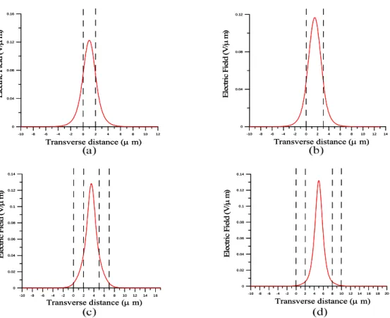
Fig. 7. For the high input power density case, electric-field distributions of the two-branch optical waveguide structure with all
Fig 8. The three-branch optical waveguide structure with uniform nonlinearity.
E le ct ri c F iel d (V /μ m) Transverse distance (μ m) -10 -8 -6 -4 -2 0 2 4 6 8 10 12 0 0.002 0.004 0.006 0.008 0.01 E le ct ri c F iel d (V /μ m) Transverse distance (μ m) -10 -8 -6 -4 -2 0 2 4 6 8 10 12 0 0.002 0.004 0.006 0.008 0.01 Transverse distance (μ m) E le ctr ic F ie ld ( V /μ m) -10 -8 -6 -4 -2 0 2 4 6 8 10 12 14 0 0.002 0.004 0.006 0.008 0.01 E lect ri c F iel d ( V /μ m) Transverse distance (μ m) -12 -8 -4 0 4 8 12 16 20 24 0 0.002 0.004 0.006 0.008 E lect ri c F iel d ( V /μ m) Transverse distance (μ m) -12 -8 -4 0 4 8 12 16 20 24 0 0.002 0.004 0.006 0.008 E lect ri c F iel d ( V /μ m) Transverse distance (μ m) -12 -8 -4 0 4 8 12 16 20 24 28 0 0.002 0.004 0.006 0.008 0.01 E lect ri c F iel d ( V /μ m) Transverse distance (μ m) -12 -8 -4 0 4 8 12 16 20 24 28 0 0.002 0.004 0.006 0.008 0.01
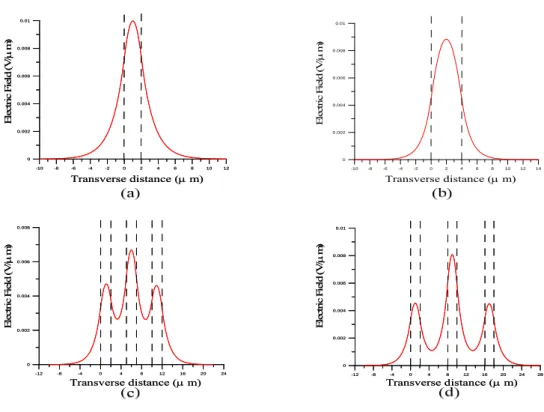
Fig. 9. For the low input power density case, electric-field distributions of the three-branch optical waveguide structure with all nonlinear
E lect ri c F ie ld ( V /μ m) Transverse distance (μ m) -10 -8 -6 -4 -2 0 2 4 6 8 10 12 0 0.02 0.04 0.06 0.08 E lect ri c F ie ld ( V /μ m) Transverse distance (μ m) -10 -8 -6 -4 -2 0 2 4 6 8 10 12 0 0.02 0.04 0.06 0.08 Transverse distance (μ m) E lect ri c F iel d ( V /μ m) -10 -8 -6 -4 -2 0 2 4 6 8 10 12 14 0 0.02 0.04 0.06 Transverse distance (μ m) E lect ri c F iel d ( V /μ m) -10 -8 -6 -4 -2 0 2 4 6 8 10 12 14 0 0.02 0.04 0.06 Transverse distance (μ m) El ec tr ic F ie ld ( V /μ m) -12 -8 -4 0 4 8 12 16 20 24 0 0.02 0.04 0.06 Transverse distance (μ m) El ec tr ic F ie ld ( V /μ m) -12 -8 -4 0 4 8 12 16 20 24 0 0.02 0.04 0.06 E le cr ic F ie ld ( V /μ m) Transverse distance (μ m) -12 -8 -4 0 4 8 12 16 20 24 28 0 0.02 0.04 0.06 0.08 E le cr ic F ie ld ( V /μ m) Transverse distance (μ m) -12 -8 -4 0 4 8 12 16 20 24 28 0 0.02 0.04 0.06 0.08
Fig. 10. For the high input power density case, electric-field distributions of the three-branch optical waveguide structure with all
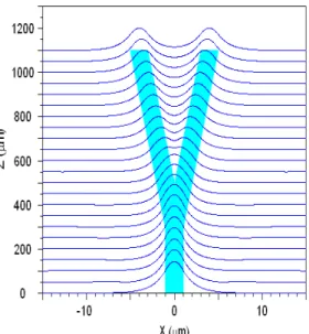
Fig. 11. The typical evolution of a wave propagating along a two-branch optical waveguide structure with all nonlinear layers at the low input power density.
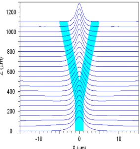
Fig. 12. The typical evolution of a wave propagating along a two-branch optical waveguide structure with all nonlinear layers at the high input power density.
Transverse distance (μ m) E le ctr ic F ie ld ( V /μ m) -10 -8 -6 -4 -2 0 2 4 6 8 10 12 0 0.02 0.04 0.06 Transverse distance (μ m) E le ctr ic F ie ld ( V /μ m) -10 -8 -6 -4 -2 0 2 4 6 8 10 12 0 0.02 0.04 0.06 Transverse distance (μ m) E le ctr ic F ie ld ( V /μ m) -10 -8 -6 -4 -2 0 2 4 6 8 10 12 14 0 0.01 0.02 0.03 0.04 0.05 Transverse distance (μ m) E le ctr ic F ie ld ( V /μ m) -10 -8 -6 -4 -2 0 2 4 6 8 10 12 14 0 0.01 0.02 0.03 0.04 0.05 E lec tr ic F iel d (V /μ m) Transverse distance (μ m) -10 -8 -6 -4 -2 0 2 4 6 8 10 12 14 16 0 0.01 0.02 0.03 0.04 E lec tr ic F iel d (V /μ m) Transverse distance (μ m) -10 -8 -6 -4 -2 0 2 4 6 8 10 12 14 16 0 0.01 0.02 0.03 0.04 E le ctr ic F ie ld ( V /μ m) Transverse distance (μ m) -10 -8 -6 -4 -2 0 2 4 6 8 10 12 14 16 18 20 0 0.01 0.02 0.03 0.04 E le ctr ic F ie ld ( V /μ m) Transverse distance (μ m) -10 -8 -6 -4 -2 0 2 4 6 8 10 12 14 16 18 20 0 0.01 0.02 0.03 0.04
Fig. 13. The relevant curves shown in Fig. 6 and 11 on the same graph
(a) at position Z1, (b) at position Z2, (c) at position Z3, (d) at position Z4,
( dotted line: the predicted results, dashed line: the numerical simulation results).
Transverse distance (μ m) E le ctr ic F ie ld ( V /μ m) -10 -8 -6 -4 -2 0 2 4 6 8 10 12 0 0.04 0.08 0.12 0.16 Transverse distance (μ m) E le ctr ic F ie ld ( V /μ m) -10 -8 -6 -4 -2 0 2 4 6 8 10 12 0 0.04 0.08 0.12 0.16 Transverse distance (μ m) E lect ri c F iel d ( V /μ m) -10 -8 -6 -4 -2 0 2 4 6 8 10 12 14 0 0.04 0.08 0.12 Transverse distance (μ m) E lect ri c F iel d ( V /μ m) -10 -8 -6 -4 -2 0 2 4 6 8 10 12 14 0 0.04 0.08 0.12 E le ctr ic F ie ld ( V /μ m) Transverse distance (μ m) -10 -8 -6 -4 -2 0 2 4 6 8 10 12 14 16 0 0.04 0.08 0.12 0.16 E le ctr ic F ie ld ( V /μ m) Transverse distance (μ m) -10 -8 -6 -4 -2 0 2 4 6 8 10 12 14 16 0 0.04 0.08 0.12 0.16 El ec tr ic F ie ld ( V /μ m) Transverse distance (μ m) -10 -8 -6 -4 -2 0 2 4 6 8 10 12 14 16 18 20 0 0.04 0.08 0.12 0.16 El ec tr ic F ie ld ( V /μ m) Transverse distance (μ m) -10 -8 -6 -4 -2 0 2 4 6 8 10 12 14 16 18 20 0 0.04 0.08 0.12 0.16
Fig. 14. The relevant curves shown in Fig. 7 and 12 on the same graph
(a) at position Z1, (b) at position Z2, (c) at position Z3, (d) at position Z4,
( dotted line: the predicted results, dashed line: the numerical simulation results).
Fig. 15. The typical evolution of a wave propagating along a three-branch optical waveguide structure with uniform nonlinearity.
Fig. 16. The typical evolution of a wave propagating along a three-branch optical waveguide structure with uniform nonlinearity.
E le ctr ic F ie ld ( V /μ m ) Transverse distance (μ m) -10 -8 -6 -4 -2 0 2 4 6 8 10 12 0 0.004 0.008 0.012 E le ctr ic F ie ld ( V /μ m ) Transverse distance (μ m) -10 -8 -6 -4 -2 0 2 4 6 8 10 12 0 0.004 0.008 0.012 Transverse distance (μ m) E lect ri c F iel d (V /μ m ) -10 -8 -6 -4 -2 0 2 4 6 8 10 12 14 0 0.002 0.004 0.006 0.008 0.01 Transverse distance (μ m) E lect ri c F iel d (V /μ m ) -10 -8 -6 -4 -2 0 2 4 6 8 10 12 14 0 0.002 0.004 0.006 0.008 0.01 El ec tr ic F ie ld ( V /μ m ) Transverse distance (μ m) -10-8 -6 -4 -2 0 2 4 6 8 1012 14 16 1820 22 0 0.002 0.004 0.006 0.008 El ec tr ic F ie ld ( V /μ m ) Transverse distance (μ m) -10-8 -6 -4 -2 0 2 4 6 8 1012 14 16 1820 22 0 0.002 0.004 0.006 0.008 El ec tr ic F ie ld ( V /μ m ) Transverse distance (μ m) -10-8-6-4-2 0 2 4 6 810121416182022242628 0 0.002 0.004 0.006 0.008 0.01 El ec tr ic F ie ld ( V /μ m ) Transverse distance (μ m) -10-8-6-4-2 0 2 4 6 810121416182022242628 0 0.002 0.004 0.006 0.008 0.01
Fig. 17. The relevant curves shown in Fig. 9 and 15 on the same graph
(a) at position Z1, (b) at position Z2, (c) at position Z3, (d) at position Z4,
( dotted line: the predicted results, dashed line: the numerical simulation results).
E le ctr ic F ie ld ( V /μ m) Transverse distance (μ m) -10 -8 -6 -4 -2 0 2 4 6 8 10 12 0 0.02 0.04 0.06 0.08 E le ctr ic F ie ld ( V /μ m) Transverse distance (μ m) -10 -8 -6 -4 -2 0 2 4 6 8 10 12 0 0.02 0.04 0.06 0.08 Transverse distance (μ m) El ec tr ic F ie ld ( V /μ m) -10 -8 -6 -4 -2 0 2 4 6 8 10 12 14 0 0.02 0.04 0.06 Transverse distance (μ m) El ec tr ic F ie ld ( V /μ m) -10 -8 -6 -4 -2 0 2 4 6 8 10 12 14 0 0.02 0.04 0.06 Transverse distance (μ m) E lect ri c F iel d (V /μ m) -10-8 -6 -4 -2 0 2 4 6 8 10 1214 16 18 2022 0 0.02 0.04 0.06 0.08 Transverse distance (μ m) E lect ri c F iel d (V /μ m) -10-8 -6 -4 -2 0 2 4 6 8 10 1214 16 18 2022 0 0.02 0.04 0.06 0.08 E lect ri c F iel d ( V /μ m) Transverse distance (μ m) -10-8-6-4-2 0 2 4 6 810121416182022242628 0 0.02 0.04 0.06 0.08 E lect ri c F iel d ( V /μ m) Transverse distance (μ m) -10-8-6-4-2 0 2 4 6 810121416182022242628 0 0.02 0.04 0.06 0.08
Fig. 18. The relevant curves shown in Fig. 10 and 16 on the same
graph (a) at position Z1, (b) at position Z2, (c) at position Z3, (d) at
position Z4, ( dotted line: the predicted results, dashed line: the