RMO2B-4
A
Low Phase Noise 52-GHz Push-Push VCO
in
0.18-pm Bulk
CMOS Technologies
Yi-Hsien
Cho,
Ming-Da Tsai, Hong-Yeh Chang, Chia-Chi Chang, Huei Wang
Dept.
of Electrical Engineering and Graduate Institute of Communication Engineering,
National Taiwan University, Taipei, 106, Taiwan, R.O.C.
Abstract
-
A V-Band fully integrated complementarypush-push VCO is first presented in 0.1S-pn bulk CMOS
technologies. Thin-film microstrip (TFMS) lines are utilized
in the circuit to reduce the conductive substrate effect. In
order to lower the phase noise, complementary cross-coupled pairs are used to generate negative conductance. The
measured phase noise at 1-MHz offset is about -97 dB& at
52.6 GHz and is -104 dBc/Hz at 26.3 GHz. To the author’s best knowledge, this complementary CMOS VCO achieves
the lowest phase noise in comparison with other VCOs using standard bulk CMOS processes in V-Band.
Jndex Terms
-
CMOS, thin-film microstrip line, VCO.I.
INTRODUCTION
The increasing demand of monolithic microwave integrated circuits (MMICs) is motivated by the rapid growth of high speed wireless communications, for example, wireless LANs and mobile phones. Voltage controlled oscillator (VCO) is an important building element in the implementation of modern wireless communication systems. For considerations of low cost and low power consumption, CMOS is the best choice for these applications. However, in microwave and millimeter-wave regime, integrated VCOs are generally realized by III-V compound devices or SiGe HBTs
[1]-[3].
CMOS VCOs found few applications due to its low maximum oscillation frequency (fm,}.As CMOS technology progresses to deep submicron, it has become possible to realize millimeter-wave circuits in standard CMOS process, leading to IOW cost and high integration. So far, some V-Band VCOs have been reported in CMOS technology [4]-[5]. A 50-GHz VCO
was
presented which adopted a modified 0.25-pm CMOS process for high quality factor inductor and highfmv: of the device 141. It shows low phase noise of -99 dBcMz at 1-MHz offset and the output power is -11 dBm. Another fully-integrated 51-GHz VCO fabricated with 0.12-pm CMOS process, demonstrated -30-dBm output power and -85 dBc/Hz phase noise at I-MHz offset [ 5 ] . Tn addition to adopting high
Lax
process technology, some other circuit structures were presented to achieve higher oscillation frequency. Push-push VCO is an attractive approach0-7S03-8983-2/05/$20.00 0 2005 IEEE
which sums up the differential fundamental signals and takes the second harmonic as the output and is even able to work above devicefmu.
In this paper, we present the first complementary push- push VCO in V-Band. The VCO core is composed of NMOS and PMOS crass-coupled
pairs
to lower the phase noise. The second harmonic output signal is taken fromtwo fundamental differential buffers working in triode region for the nonlinearity which deliver more output power. Compared with the conventional topology, the circuit delivers 14 dB more
Yd
harmonic output power in our approach from simulations. The MMIC VCO achieves very low phase noise of -97dBc/Hz at 1-MHz offset with a tuning range of 0.5GHz.
Table 1 summarizes the comparison among previously published MMW VCOs using silicon-based processes and this work. It can be observed that OUT chip demonstrated
the lowest phase noise and comparable chip
size,
power consumption and output power among the reported VCOs using standard bulk CMOS processes in V-Band.11. CMOS CHARACTERIST~CS AND PROCESS The chip is implemented by TSMC’s
0.18-ym
commercial process C61-171, with a 2-pm AlCu top metal layer. The substrate conductivity is approximately 10 S/m. With optimized
CMOS
technology and deep n-well, this technology provides f, andf- better than 60 and 55GHz,
respectively. MIM capacitors with 1
fF/pm’
are also provided in the process.111. CIRCUIT DESlGN
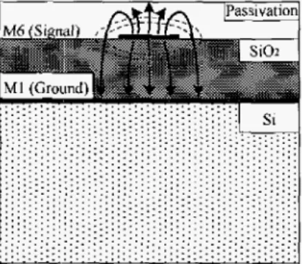
Figure 1 shows the structure of the thin-film microstrip (TFMS) line which consists of the 2-pm AlCu top metal ( M 4 ) as the signal line and bottom metal (MI) as ground plane in the 0.l8-ptn CMOS process. The
TFMS
line has the advantage of the ground plane shielding to isolate the conductive substrate. The substrate thickness ofTFMS
line is about 6.52-ym, thus the coupling effect between transmission lines is negligibk. Therefore, the matching dements of transmission lines and inductors can be132
TABLE 1
COMPARISON WITH PREVIOUSLY REPORTED VCOS IN V-BAND
Process
0.25-pm SiGe
BiCMOS
SiGe HBT
Frequency Phase noise @ I MHz Chip Size Poc Pout
(GHzt) offset ( d E c m t ) ("'1 (mw) ("1 60 -87 ' 0 . 4 ~ 0 . 7 5 73.8 -17 76 -9 I 0.4 xO.75 128 -7 50 -98 N/A N/A -5.6 -92
1
0.3x0.25I
211
-6.8 0.09-pm CMOS 0.18-pm CMOS 0.25-pm CMOS I I I I I I 52.5 -86 0.8 x 1 41 -8 63 -86 0.45 x 0.7 118.8 -4 Modified1
0,25-pmCMOS1
501
-991
0 . 5 2 x 0 . 3 9I
131
-11 Complementary cross- coupled and push-pushI I I I I
I
I This Work1
0.12-pm CMOS1
5 1I
-85I
0.5x0.9I
1I
-30I
0.18-pmCMOSI
52I
-971
0.45 x 0.45 27.3 -16 replaced by meandering TFMS lines in a very small areato reduce the circuit size. A full-wave EM simulation tool, Sonnet
[SI,
was used to estimate the impedance of theTFMS
inductors over the frequency of interest.Fig. 1. The structures of the TFMS on bulk CMOS process.
The conventional cross-coupled push-push VCO circuit structure is shown in Fig. 2 where it adopts NMOS cross- coupled pair to generate negative conductance and the output signal is delivered from the middle of the inductor of the LC tank where the differential fundamental signals cancel out each other and the second harmonic signals combine i n phase [9]-[10].
Complementary cross-coupled pairs show lower phase noise because it has larger voltage swing within the LC tank and it shows more symmetric effective impulse sensitivity function [ 111. Unfortunately, the
f,,
of PMOS is usually much lower than NMOS so that it can not beTopalogy Push-push Cross-coupled 1141 Cross-coupled Cross-coupled Single-ended 1131 Cross-coupled and DUh-DUh
used in millimeter-wave regime. But for push-push VCO, we can still use PMOS to make the VCO oscillate at fundamental frequency and deliver the 2* harmonic signal to achieve low phase noise in high frequency. Figure 3 shows the circuit schematic of our design. The LC tank is composed of the TFMS differential inductors and NMOS connected as varactors. We omit the current source to lower the phase noise such that the noise from current source can be eliminated and tank voltage swing can be increased [12]. In addition, the negative conductance is generated by complementary cross-coupled pairs consisting of M,-M, to lower the phase noise. In this design, if we remove the PMOS cross-coupled pair
(M,
and M,) and maintain the DC current, the phase noise degrades by about 3 dB from the simulation results.
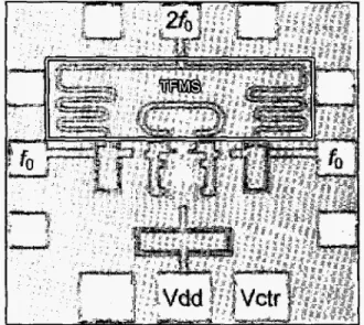
The circuit can deliver both fundamental and second harmonic signals simultaneously. The fundamental 26- GHz output signals are delivered through common-source buffers. Unlike the conventional push-push topology where the 2"d harmonic signal is extracted from the virtual short point inside the resonant tank, the 2" harmonic signal is first amplified through buffers
(M,
andM,)
and taken from the middle of TFMS inductors (L, and L,). To acquire more output power, M, and M, are biased in triode region, and therefore, with the increased device nonlinearity, the Znd harmonic power can be increased. From the simulations, it delivers 14 dB more 2nd harmonic output power in our approach than the conventional one in which the output is taken from the middle of the inductor of the LC tank, that is, from point A shown in Fig. 3.fo!
+
Fig. 2. Schematic of conventional NMOS-only cross-coupled
PUSh-pUSh VCO.
Fig. 3. Schematic ofproposed VCO.
Iv. MEASUREMENT RESULTS
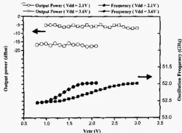
This chip was tested via on-wafer probing and was biased by aluminum bond wires. The VCO core draws 13 mA at 2.1 V and the buffer amplifiers draw 4 mA at 0.3 V. The measured output power is about -16 dBm and the oscillation frequency
is
from52.6
to 52GHz
with controlvoltage (VJ from 0.8 to 2.1 V. When we increase the VCO bias voltage up to 3.6 V with 34 mA and the buffers draw 19 mA at 0.7 V, the output power goes up to
-5
dBm. And the oscillation frequency is from 52.5 to 52 GHz with control voltage ( V J from 1 to 3 V. Figure 4 shows the output power and oscillation frequency versus control voltage in both bias conditions. The measured phase noise is -97 dBc/Hz at 1-MHz offset at 53 GHz and -104 dBcMz at 26.5 GHz as shown in Fig. 5 and Fig. 6 respectively. The measured fundamental power from the 2nd harmonic output is -58.6 dBm shown in Fig. 7 with20
dB
cable and transition loss, that is, the fundamental rejection is about 30 dB. Figure 8 shows the chip photo and the size is 0.45 x 0.45 mm2 including all test pads.’1 - 0 u t p u f P o w e r ~ V d d ~ I . l V l +Frequeory(Vdd=Z.lVj 40utputPower( Vdd=3.6V) -Freqwncy( V d d E 3 . W ) 0- -5
-
-
-la;+
1.5 2.0 2.5 3.0 3.5 0.5 1 .o Vctr (v)Fig.
4.
Measured output power versus control voltage.V. CONCLUSION
This paper presents the design and measurement of a 52 GHz complementary push-push VCO using a standard CMOS 0.18-ym process. The chip shows very low phase noise of -97 dBc/Hz at 1-MHz offset at 52 GHz with 0.5-
GHz tuning range. The output power is about -16 dBm while dissipating 27.3-mW dc power. This chip shows a
miniature size of 0.45 x
0.45
mm2. To
the bestof our
knowledge, the VCO achieves the lowest phase noise in V-Band in comparison with other VCOs in standard CMOS process.
ACKNOWLEDGEMENT
This work is supported in part by National Science Council of Taiwan, R.0.C (Projects NSC 93-22 19-E-002- and
NSC 93-2752-E-002-002-PAE). The chip was
fabricated by TSMC through the Chip Implementation Center (CIC) of Taiwan,
R.O.C.
016, NSC 93-2219-E-002-024, NSC 93-2213-E-002-033,
A Mkrl 1.08 MHr
Ref B dBm Ext MIX Noise -96 96 dB/Hz
Res BN 91 kHz *WBN 3 kHz Sweep 28 6 ms (601 pts)
Fig. 5 Measured phase noise at 1 MHz offset
Center 26.366 7 GHr
#Res BW i B B kHz
Span 508 HHz- iUBW 3 kHz
Fig. 6 . Measured fundamental power from 2”* harmonic output.
Sweep 1.3 s (601 pts)
REFERENCES
W. Winkler, J. Borngraber, B. Meinemann and P. Weger, “60GHz
and 76GHz oscillators in 0.2Slspl m d m SiCe:C BiCMOS,” in
IEEE h i . Solid-Stare Circuii ConJ Dig. Tech. Papers, pp. 454-455, 2003.
F. X. Sinnesbichler, H. Gebinger, G. R. Olbrich, “A 50 CHz SiGe
HBT push-push oscillator,” in IEEE Int. Microwme S y ” . Dig., pp. 9-12, 1999.
F. Lenk et al., “Low Phase-Noise Monolithic GalnPKaAs-HBT VCO for77GHz,” IEEE MTT-S In!. Microwme Symp. Digest, Vol.
2, pp. 8-13,June2003.
HongMo Wang, “A 50 GHz VCO in 0.25 Frn CMOS,” in IEEE Int.
Solid-Stare Circuit Conf Dig. Tech. Papers, pp. 372-373,2001.
M. Tiebout, H.D. Wohlmuth and W. Simburger, “A 1 V SlGHz
fitlly-integrated VCO in 0. I2 pm CMOS,” in IEEE Int. Solid-State Circuir CO@ Dig. Tech. Papers, pp. 300468,2002.
H. M. Hsu, et al, “A 0.18-pm foundry RF CMOS technology with 70-GHz Ft for single chip system solutions,” IEEE Inlernarional
Microwave Symp. Digest, pp. 1869-1872,2001.
C. H. Diaz, et al., “A 0.18-pm CMOS logic technology with dual gate oxide and low-k interconnect for high-performance and low-
power applications,” IEEE YLSI Tech. Symp., pp. I 1-12, 1999. http://www,sonnetusa.com.
Chia-Chi Chang, Ren-Chieh Liu, and Huei Wang, “A 40-GHz
push-push VCO using 0.25-pn CMOS technology, in 2003 Asio-
Pacijc Microwave Conference Proceedings, Vol. 1, pp. 73-76,
2003.
Ren-Chieh Liu, Hong-Yeh Chang, Chi-Hsueh Wang and Huei
Wang, “ A 63-GHz VCO using a standard 0.25-pm CMOS process, ” in IEEE Inf. Solid-State Circuit Cant Dig. Tech. Papers, pp. 372-373,2004.
[ I l l R. Apricio, A. Majimiri, “A CMOS Differential Noise Shifting Colpitts VCO,” in IEEE Inf. Solid-State Circuit Conf Dig. Tech. Papers, vol.1, pp. 3-7,2002.
[I21 P. Andreani, H. Sjoland, “Tail current noise suppression in RF
CMOS VCOs,”lEEE J. Solid-Sfute Ckcuifs, Vol. 37 no. 3, pp.342-
348, Mar. 2002.
[I31 H. Shigematsu, T. Hirose, F. Brewer and M. Rodwell, “CMOS
circuits design in millimeter-wave applications,” in IEEE Rudio Frequency Integrated Circuits Symp. Rig. pp. 123-126,2003,
[I41 F. Ellinger, T. Morf, G. Buren, C. Kromer, G. Sialm, L. Rodoni, M Schmatz and H. Jackel, “60 CHz VCO with wideband tuning range
fabricated on VLSI SO1 CMOS technology,” in IEEE M7T-S Int. Microwme Symp. Dig, Vol. 3, pp. 1329-1332,2004,
Fig. 7. Chip photo of the push-push VCO with a chip size of
0.45 x 0.45 mm’.