國 立 交 通 大 學
電信工程研究所
碩 士 論 文
以非對稱直交分合波器
設計跨接耦合器及其雙頻設計
New Crossover Coupler Design Using Asymmetric
Branch-Line Hybrids and Its Dual-Band Operation
研究生:詹麒宏 (Chi-Hung Chan)
指導教授:郭仁財 博士 (Dr. Jen-Tsai Kuo)
以非對稱直交分合波器
設計跨接耦合器及其雙頻設計
New Crossover Coupler Design Using Asymmetric
Branch-Line Hybrids and Its Dual-Band Operation
研究生:詹麒宏 Student:Chi-Hung Chan
指導教授:郭仁財 博士 Advisor:Dr. Jen-Tsai Kuo
國立交通大學
電信工程研究所
碩士論文
A Thesis
Submitted to Department of Communication Engineering
Institute of Electrical and Computer Engineering
National Chiao Tung University
In partial Fulfillment of the Requirements
for the Degree of
Master of Science
In
Communication Engineering
July 2010
Hsinchu, Taiwan, Republic of China
中華民國 九十九 年 七 月
以非對稱直交分合波器
設計跨接耦合器及其雙頻設計
研究生: 詹麒宏 指導教授: 郭仁財 教授
國立交通大學 電信工程研究所
摘要
本論文研究串接兩個任意功率輸出比例的非對稱分波直交耦合器,設
計跨接耦合器。每一個耦合器兩個對角端埠可具有不一樣的負載阻抗。由
於電路有數個設計自由度,本文以區塊 ABCD 矩陣分析,以預測跨接耦合
器的頻寬。
為了讓跨接耦合器具有雙頻功能,本文引用一個基本雙埠單元,取代
直交分波耦合器中的四分之一波長傳輸線。此雙埠基本單元包含一段步階
式阻抗線段及其末端的兩個並聯傳輸線殘段。利用傳輸線理論,列出解析
方程式並求電路參數解。本文實作一個 0.9/1.8 GHz 的跨接耦合器電路,並
加以量測以驗證本文所提之設計。
New Crossover Coupler Design Using Asymmetric
Branch-Line Hybrids and Its Dual-Band Operation
Student:Chih-Hung Chan Advisor:Dr. Jen-Tsai Kuo
Institute of Communication Engineering
National Chiao Tung University
Abstract
Two asymmetric branch-line hybrids with arbitrary power divisions are cascaded for design of a crossover coupler. The two pairs of the diagonal ports are allowed to have different characteristic impedances. Block ABCD matrices are applied to estimate the bandwidth of the crossover coupler.
To achieve the dual-band operation, an elementary two-port is employed to replace the /4-section of each hybrid. The two-port consists of a stepped-impedance section with two open stubs shunt at both of its ends. By means of the transmission-line theory, analytical equations are formulated to solve the circuit parameters. A circuit designed at 0.9/1.8 GHz is realized and measured to validate the idea.
Acknowledgement
致謝
研究所這兩年,從無到學富微波知識,最感謝的是我的指導教授,郭
人財老師,謝謝老師耐心指導駑鈍如我這般的學生,總是比我還仔細想著
研究的每個細節,想法總是那麼富有創意,跟著老師一步一步學,到如今
我也能有自己的研究方式和態度,這是我學到最寶貴的資產。同時感謝百
忙抽空前來的口試委員:張盛富老師、鐘世忠老師和金國生老師,對學生
研究進一步的討論和指導,讓我有更進步的空間。
同時,實驗室同學們,若沒你們的支持和幫助,我根本不可能這麼順
利完成論文。逸群學長和裕豪學長,你們學富五車的知識讓我能盡情從你
們身上挖掘,當研究遇到瓶頸時,你們就像沙漠綠洲、久旱甘霖般滋養著
學弟妹們。紹展、卓諭、餃妹、狗狗、宣融、組偉、小尻、佑先,很開心
這段時間大家的相伴,一起學習和討論,互相取笑和打鬧,人家常說志同
道合的夥伴最是難得。希望大家離開實驗室之後,各自發展宏圖,理想與
現實合而為一,多年之後能光耀實驗室門楣。還有在職班的學長們,志銘
學長、其昌學長和書賢學長,在我探路職場能給我一些經驗談,使我對漫
漫前路有一點方向,不會那麼徬徨無助。
最後我想感謝自己的家人,因為研究繁忙,總是無法常回家,沒辦法
好好的陪伴在你們身旁,有時候也不常打電話回去。反到是你們時常的關
心,讓我身處遠離家鄉也有家鄉的溫暖。從襁褓到成熟的成年人了,人生
一切都是由家裡提供養分讓我茁壯,謝謝你們。
Contents
Chapter 1 Introduction1.1 Literature Review---1
1.2 Contributions---2
Chapter 2 Crossover Coupler Design using Asymmetric Branch-Line Hybrids 2.1 Crossover Coupler Design---4
2.1.1 Asymmetric Branch-Line Hybrid with Arbitrary Termination Impedances---5
2.1.2 Two Asymmetric Branch-Line Hybrids in a Cascade---6
2.2 Circuit Bandwidth ---8
2.2.1 Block ABCD matrix for Four-Port Network---8
2.2.2 Conversion between the Block ABCD matrix and the 4×4 Y matrix---10
2.2.3 Bandwidth Calculation---15
2.3 Simulation and Measurement---27
Chapter 3 Dual-Band Crossover Coupler Design 3.1 Elementary Two-Port Network for Dual-Band Operation---32
3.2 Simulation and Measurement---35
Chapter 4 Conclusion Conclusion---40
List of Figures
Figure 2.1 Circuit schematic of an asymmetric branch-line hybrid.---5
Figure 2.2 (a) Proposed crossover coupler with arbitrary diagonal termination impedances.
(b) Analysis of (a) by the transmission line model.---7
Figure 2.3 (a) Voltage and current definitions in Z- and Y-parameter formulations.
(b) Voltage and current definitions in block ABCD parameter
formulations.---9
Figure 2.4 Block ABCD matrices for analysis of a cascade of two four-ports.---10
Figure 2.5 Circuit schematic of a four port coupler.---17
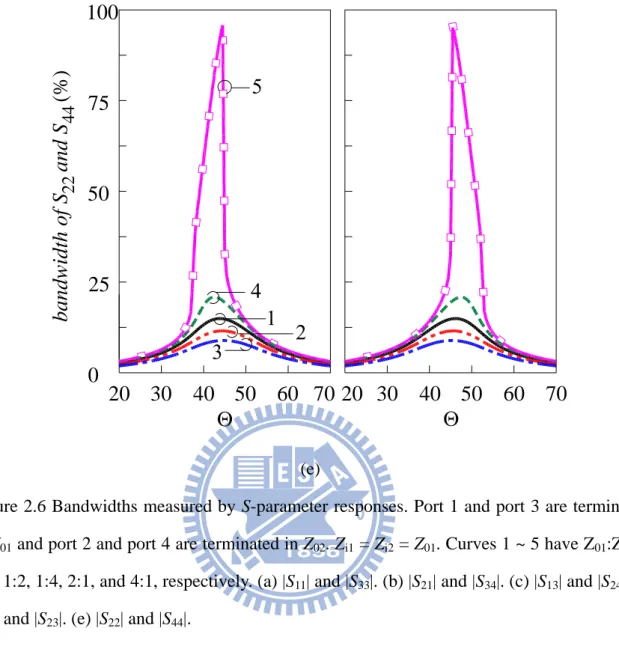
Figure 2.6 Bandwidths measured by S-parameter responses. Port 1 and port 3 are terminated
in Z01 and port 2 and port 4 are terminated in Z02. Zi1 = Zi2 = Z01. Curves 1 ~ 5
have Z01:Z02 = 1:1, 1:2, 1:4, 2:1, and 4:1, respectively. (a) |S11| and |S33|. (b) |S21|
and |S34|. (c) |S13| and |S24|. (d) |S14| and |S23|. (e) |S22| and |S44|.---20
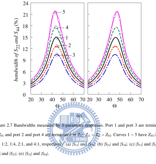
Figure 2.7 Bandwidths measured by S-parameter responses. Port 1 and port 3 are terminated
in Z01 and port 2 and port 4 are terminated in Z02. Zi1 = Zi2 = Z02. Curves 1 ~ 5
have Z01:Z02 = 1:1, 1:2, 1:4, 2:1, and 4:1, respectively. (a) |S11| and |S33|. (b) |S21|
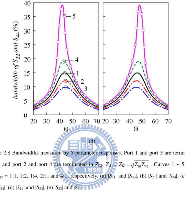
Figure 2.8 Bandwidths measured by S-parameter responses. Port 1 and port 3 are terminated
in Z01 and port 2 and port 4 are terminated in Z02. Zi1 = Zi2 = Z Z01 02 . Curves
1 ~ 5 have Z01:Z02 = 1:1, 1:2, 1:4, 2:1, and 4:1, respectively. (a) |S11| and |S33|.
(b) |S21| and |S34|. (c) |S13| and |S24|. (d) |S14| and |S23|.
(e) |S22| and |S44|.---26
Figure 2.9 The S-parameters of the first fabricated circuit with Zo1 = 25 , Zo2 = 100 ,
Zi = 100 and 46. (a) |S11|, |S21|, |S31|, |S41|. (b) |S22|, |S23, |S33|. (c) |S24|, |S34|,
|S44|. (d) The circuit photo. W1 ~ W7 are 2.06, 0.48, 1.01, 1.1, 1.18, 0.43 and
2.19 mm. L1 ~ L7 are 11.06, 11.69, 11.42, 11.39, 11.35, 11.72 and 11.02
mm.---29
Figure 2.10 The S-parameters of the second fabricated circuit with Zo1 = 100 , Zo2 = 50 ,
Zi = 50 and 40. (a) |S11|, |S21|, |S31|, |S41|. (b) |S22|, |S23, |S33|. (c) |S24|, |S34|,
|S44|. (d) Circuit photo. W1 ~ W7 are 1.33, 1.84, 0.74, 3.74, 0.26, 2.49 and 0.92
mm. L1 ~ L7 are 11.29, 11.12, 11.55, 10.7, 11.85, 10.95 and 11.47
mm.---31
Figure 3.1 Two-port network for subsituting a quarter-wave section.---34
Figure 3.2 Design graphs for determining s1 and R. (a) s2 = 5o. (b) s2 = 10o. Both s1 and
Figure 3.3 Two cascaded asymmetric branch-line hybrids to form a new crossover coupler
with arbitrary diagonal port impedances Zo1 and Zo2.---36
Figure 3.4 Simulation and measured responses of the fabricated dual-band crossover
junction. (a) |S11| and |S41|. (b) |S21| and |S31|. (c) |S22| and |S32|. (d) |S12| and |S42|.
Zo1 = 50 and Zo2 = 25 . (e) Photograph of the experimental
Chapter 1
Introduction
Crossover is an essential device for microwave and radio frequency integrated circuits. In a microstrip circuit [1], an air-bridge interconnect is an intuitive solution, and this three- dimensional structure exhibits a low-pass characteristic. In [2], two signal traces are laid on different metal layers and an additional grounded plane is placed in between to shield one signal from the other. One can expect that extra vias are required to have all the input and output terminals of the crossover in one metal plane. Obviously, if a fully planar crossover coupler can be realized with ideal transmission loss, return loss and isolation, not only the vias mentioned above and hence the fabrication cost, can be saved, but also the overall circuit performance can be enhanced.
1.1 Literature Review
To reduce the design complexity, a series of fully planar multi-port couplers with crossover applications have been investigated in [3-9]. Ideally, the crossover junction is supposed to provide 0-dB insertion loss to diagonal ports and perfect isolation to adjacent ports. In [3], microstrip and stripline crossovers are contrived on the basis of two cascaded branch-line hybrids. In [4], octave-wide matched symmetrical and reciprocal four- and five-port networks are proposed. A circular disk can also be designed as a symmetrical and reciprocal four-port crossover junction [5]. In [6], a novel planar configuration of 0-dB directional coupler is presented as a single-layer crossover in microwave integrated circuits. The circuit configured in a “window”-shape [7] may have an improved bandwidth if the characteristic impedances of the constitution branches can be properly designed. Recently, in [8-9], a double-ring structure is proposed for design of microstrip four-port crossover coupler.
The eigenmode model is developed for analysis to investigate the circuit performance. The measured data of the circuit show that the isolation and return loss of the prototype coupler exceed 20 dB over a bandwidth of 20%. In [10], a four-port crossover coupler with a simpler configuration is proposed and investigated.
Recent rapid progress in wireless communication systems has created a need of dual-band operation for RF devices [13-19]. In [13], a rigorous design is presented for microstrip bandpass filters with a dual-passband response in parallel-coupled and vertical-stacked configurations. In [14], a novel branch-line coupler is proposed to operate at two arbitrary frequencies with additional stubs. In [15], a two-port consisting of a stepped-impedance section with open stubs attached to its two ends is proposed to imitate the 90o-section at the two designated frequencies with different characteristic impedances. In [16], novel arbitrary dual-band microwave components based on components using right/left hand transmission lines have been presented. In [17], a novel elementary two-section impedance transformer has been shown to be capable of dual-band operation under unrestricted load and frequency conditions. In [18], a new dual-band 3 dB three-port power divider based on a two-section transmission-line transformer for arbitrary impedance terminations is proposed. In [19], two novel PIFA-related dual-band antennas with spiraled and coupled structures have been proposed and demonstrated. Note that all crossover junctions in [1]-[10] are designed to have identical diagonal port impedances and operate in a single passband. Thus, this thesis studies the dual-band design of the crossover junction based on the approach employed in [15]. Design graph will be provided.
1.2 Contribution
Crossover coupler can also be designed using two branch-line hybrids in a cascade [3]. By applying standard hybrid analysis techniques, theoretically, the signal emerges only at the
diagonal port of the composite structure, with no insertion loss, and no power emerges from the remaining two ports such that high isolation between two crossing signal channels can be achieved. Nevertheless, the design is limited to that the two crossover traces have identical characteristic impedances. Chapter 2 extends the realization of planar crossover coupler of which the two crossover signal traces are allowed to have different characteristic impedances. The circuit consists of two asymmetric branch-line hybrids [11-12] in cascade. Each hybrid is designed to have arbitrary power division and termination impedances. By properly selecting the structure parameters of each hybrid, a crossover coupler could be readily fulfilled. Measured results of a fabricated circuit agree very well with the simulated counterparts.
In Chapter 3, the design of crossover junction with unequal port impedances in Chapter 2 is extended to have a dual-band characteristic based on the approach in [16]. According to the best of our knowledge, this is the first dual-band crossover coupler in open literature, so that its performance deserves investigation. An experimental microstrip dual-band crossover coupler is simulated and measured for demonstration.
Chapter 2
Crossover Coupler Design using Asymmetric Branch-Line
Hybrids
Crossover coupler is one of the solutions to the problem that two transmission lines cross each other. It enables the two signal paths to have as low as interference with each other. This chapter presents a crossover coupler design based on two asymmetric branch-line hybrids with arbitrary power divisions in a cascade. It is a new idea to design a four-port crossover junction with different termination impedances. Block ABCD matrix formulation is applied to the circuit to estimate the bandwidth. The relation between power division ration of asymmetric branch-line hybrids and performance of the crossover coupler is also investigated.
2.1 Crossover Coupler Design
A crossover coupler can be designed using two branch-line hybrids in a cascade [3]. By applying standard hybrid analysis techniques, theoretically, the signal emerges only at the diagonal port of the composite structure, with no insertion loss, and no power emerges from the remaining two ports so that high isolation between two crossing signal channels can be achieved. Nevertheless, the design has hitherto been limited to that the two crossover traces have identical characteristic impedances. This Chapter extends the realization of planar crossover coupler of which the two crossover signal traces are allowed to have different characteristic impedances. The circuit consists of two asymmetric branch-line hybrids [12-13] in cascade. Each hybrid is designed to have arbitrary power division and termination impedances. By properly selecting the structure parameters of each hybrid, a crossover coupler can be readily fulfilled.
2.1.1 Asymmetric Branch-Line Hybrid with Arbitrary Termination Impedances
In [11-12], an asymmetric branch-line coupler with arbitrary termination impedance and
arbitrary power division is proposed. Figure 2.1 shows this four port coupler terminated in arbitrary impedances Za, Zb, Zc and Zd. It consists of four -sections which form a ring. The impedances of four -sections are Z1, Z2, Z3 and Z4. When power is fed into port 1, phase difference of the two output waves at port 2 and port 3 is 90o. The ratio |S21|/|S31| is d1/d2 while port 4 is isolated. The design equations are as follows. For Za = Zb = Zc = Zd and d1 = d2, the result is the well-known conventional branch-line coupler [3].
2 1 1 2 2 1 2 a b d Z Z Z d d (2.1a) 1 2 2 b c d Z Z Z d (2.1b) 2 1 3 2 2 1 2 c d d Z Z Z d d (2.1c) 1 4 2 d a d Z Z Z d (2.1d)
3
2
4
1
bZ
Z
d cZ
Z
aZ
4 3Z
Z
2 1Z
Figure 2.1 Circuit schematic of an asymmetric branch-line hybrid.2.1.2 Two Asymmetric Branch-Line Hybrids in a Cascade
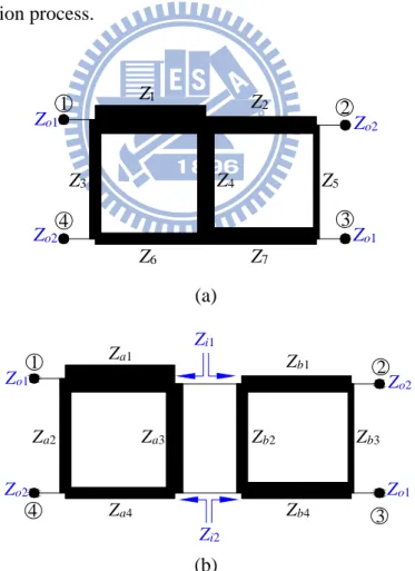
Figure 2.2(a) shows the schematic of the proposed crossover coupler. It consists of seven quarter-wavelength sections with characteristic impedances Z1 ~ Z7. The termination impedances of the two pairs of the diagonal ports are Zo1 and Zo2. The circuit can be treated as
two cascaded asymmetric branch-line hybrids as shown in Figure 2.2(b). Each hybrid possesses arbitrary power division and termination impedances. For impedance matching purpose, the two output terminations of the first hybrid, Zi1 and Zi2, are designed to be the
same as the two input counterparts of the second circuit. Since the sections Za3 and Zb2 are in
shunt connection, we have Z4 = Za3//Zb2. For coupler i (i = 1, 2) at the center frequency, let the
outputs at their individual through and coupled ports be designated as –ji and –i,
respectively. Here, i and i are positive real numbers satisfying i2 + i2 = 1. Applying the
standard hybrid analysis technique, we have
21 ( 1)( 2) ( 1)( 2) 1 2 1 2
S j j (2.2a)
31 ( 1)( 2) ( 1)( 2) ( 1 2 1 2)
S j j j (2.2b)
Note that the design specifications require that |S11| = |S21| = |S41| = 0 and |S31| = 1. After some algebraic manipulation, it can be validated that 1 = 2 and 1 = 2. By employing the design equations in [3] and [12], the characteristic impedances of the branch-line sections can be written as 1 1 1sin a o i Z Z Z (2.3a) 2 1 2 tan a o o Z Z Z (2.3b) 3 1 2 tan a i i Z Z Z (2.3c) 4 2 2 sin a i o Z Z Z (2.3d)
1 2 1cos b o i Z Z Z (2.4a) 2 1 2 cot b i i Z Z Z (2.4b) 3 1 2cot b o o Z Z Z (2.4c) 4 2 1cos b i o Z Z Z (2.4d)
where sin = 1 and cos = 1. From (2.3) and (2.4), provided that Zo1 and Zo2 are known,
Zak and Zbk (k = 1, 2, 3 and 4) can be readily obtained once , Zi1 and Zi2 are given.
Consequently, there are several degrees of freedom for the design since , Zi1 and Zi2 can be
arbitrary. The only concern for choosing their values should be the realization of the line widths of the fabrication process.
Z1 2 Z 3 Z Z4 Z5 Z7 6 Z o1 Z Zo2 Zo1 Zo2 1 2 3 4 (a) 3 2 4 1 Zi2 i1 Z Zb2 o2 Z Zo1 o2 Z Zo1 Za4 Zb4 Zb3 a3 Z Za2 Zb1 a1 Z (b)
Figure 2.2 (a) Proposed crossover coupler with arbitrary diagonal termination impedances. (b) Analysis of (a) by the transmission line model.
2.2 Circuit Bandwidth
2.2.1 Block ABCD Matrix for Four-Port Network
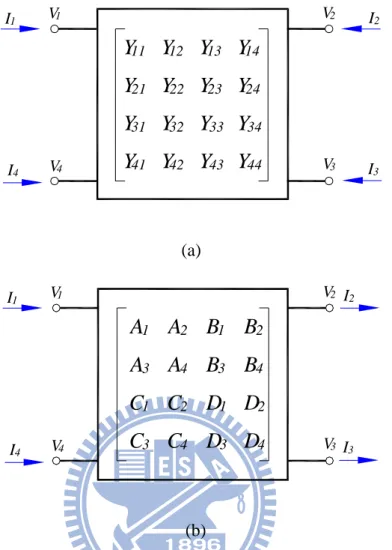
In Figure 2.3 (a) and (b), port voltages and currents are defined at various terminals of a four-port network for Y-, Z- and ABCD-parameter analyses. Admittance and impedance matrices are used to describe the relation between the port voltages and currents in Figure 2.3 (a). The admittance matrix [Y] of the microwave network relates these voltages and currents as shown in (2.5):
11 12 13 14 1 1 1 21 22 23 24 2 2 2 31 32 33 34 3 3 3 41 42 43 44 4 4 4 Y Y Y Y I V V Y Y Y Y I V V Y Y Y Y Y I V V Y Y Y Y I V V (2.5)The impedance matrix can be defined in a similar fashion. The matrices [Y] and [Z] can be used to characterize a microwave network, but in practice when a microwave network consists of a cascade of two or more four-port networks, it is convenient to use a 4-by-4
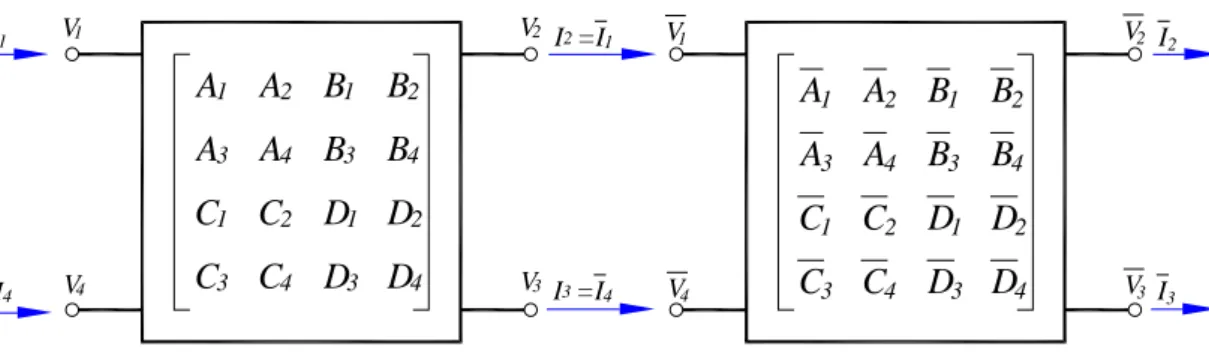
ABCD-parameter for analysis purpose. The ABCD matrix of the cascade of two or more
four-port can be easily obtained by directly multiplying the ABCD matrices of the each four-port, as shown in Figure 2.4. Mathematically, the voltages and currents of the two ports on the left hand side of the network are related to those on the right hand side by (2.6):
1 2 1 2 2 1 3 4 3 4 3 4 1 2 1 2 2 1 3 4 3 4 3 4 A A B B V V A A B B V V C C D D I I C C D D I I (2.6)
1 I 4 I 2 I 3 I 1 V 4 V 2 V 3 V 41
Y
31Y
21Y
11Y
42Y
32Y
22Y
12Y
43Y
33Y
23Y
13Y
44Y
34Y
24Y
14Y
(a) 1 I 4 I 2 I 3 I 1 V 4 V 2 V 3 V 3C
1C
3A
1A
4C
2C
4A
2A
3D
1D
3B
1B
4D
2D
4B
2B
(b)Figure 2.3 (a) Voltage and current definitions in Z- and Y-parameter formulations. (b) Voltage and current definitions in block ABCD parameter formulations.
For the voltages and currents of a four-port in the block ABCD-parameter formulation shown in Figure 2.3 (b), the directions of currents at port 2 and port 3 are opposite to those in the Y- and Z-parameter formulation. By using similar definition for the traditional two-port ABCD matrix, each of the Ai-entries in block ABCD can be determined by applying input voltages at port 1 and port 4, and measuring the open-circuit output voltages at port 2 and port 3. Similarly, each entry in block B is the ratio of input voltages to short-circuit output currents, those in block C is the ratio of input currents to open-circuit output voltages, and those in block D is the ratio of input currents to short-circuit currents. Detailed derivations are given in the following subsections.
1 I 4 I 2 I =I 3 I =I 1 V 4 V 2 V 3 V 3 C 1 C 3 A 1 A 4 C 2 C 4 A 2 A 3 D 1 D 3 B 1 B 4 D 2 D 4 B 2 B 2 I 3 I 1 V 4 V 2 V 3 V 3 C 1 C 3 A 1 A 4 C 2 C 4 A 2 A 3 D 1 D 3 B 1 B 4 D 2 D 4 B 2 B 1 4
Figure 2.4 Block ABCD matrices for analysis of a cascade of two four-ports.
2.2.2 Conversion between the Block ABCD Matrix and the 4×4 Y Matrix
From (2.6), we have 3 2 3 1 1 0, 0, 0 2 |V I I V A V . (2.7)
Substituting V3 = 0, I2 = 0 and I3 = 0 into the relation of voltages and currents in the Y matrices, we have
I2 Y V21 1Y V22 2Y V24 4 0 (2.8a)
3 31 1 32 2 34 4 0
I Y V Y V Y V (2.8b)
Multiplying (2.8a) by Y34 and subtracting (2.8b) multiplied by Y24 from it, we can eliminate V4 and obtain the relation between V1 and V2. Then the transformation of Y-parameters to A1 can be derived as shown in (2.9a). All other elements of block A can also be derived similarly and are given in (2.9b) ~ (2.9d).
32 24 22 34 1 21 34 31 24 Y Y Y Y A Y Y Y Y (2.9a) 33 24 23 34 2 21 34 31 24 Y Y Y Y A Y Y Y Y (2.9b) 22 31 32 21 3 21 34 31 24 Y Y Y Y A Y Y Y Y (2.9c) 23 31 33 21 4 21 34 31 24 Y Y Y Y A Y Y Y Y (2.9d)
From (2.6), B1 of block B is defined as
2 3 3 1 1 0, 0, 0 2 |V V I V B I (2.10)
According to the relation of voltages and currents in the Y-matrix, the following equations can be derived with V2 = 0, V3 = 0 and I3 = 0:
3 31 1 34 4 0
I Y V Y V (2.11a)
2 21 1 24 4
I Y V Y V
(2.11b)
Note that the direction of I2 in the Y-matrix is opposite to that in the block ABCD matrices. The relation of V1 and V4 in (2.11a) is used in (2.11b). Then, the ratio V1/I2 can be derived as shown in (2.12a). Similarly, all other elements block B can be obtained as follows:
34 1 21 34 31 24 Y B Y Y Y Y (2.12a) 24 2 21 34 31 24 Y B Y Y Y Y (2.12b) 31 3 21 34 31 24 Y B Y Y Y Y (2.12c)
21 4 21 34 31 24 Y B Y Y Y Y (2.12d)
From (2.6), C1 of block C is defined as
3 2 3 1 1 0, 0, 0 2 |V I I I C V (2.13)
According to the relation of voltages and currents in the Y-matrix and the conditions V3 = 0, I2 = 0 and I3 = 0, the following equations can be derived:
2 21 1 22 2 24 4 0 I Y V Y V Y V (2.14a) 3 31 1 32 2 34 4 0 I Y V Y V Y V (2.14b) 1 11 1 12 2 14 4 I Y V Y V Y V (2.14c)
(2.14a) and (2.14b) can be used to eliminate V4 and express V1 as a function of V2. Similarly,
V4 can be expressed as a function of V2. Applying these relations to (2.14c) can eliminate V1 and V2. Then, the ratio of I1/V2 can be obtained as shown in (2.15a). All other elements of block C can also be derived as shown in (2.15b) ~ (2.15d):
11 32 24 22 34 14 22 31 32 21 1 12 21 34 31 24 ( ) ( ) Y Y Y Y Y Y Y Y Y Y C Y Y Y Y Y (2.15a) 11 34 23 24 33 14 21 33 31 23 2 13 21 34 31 24 ( ) ( ) Y Y Y Y Y Y Y Y Y Y C Y Y Y Y Y (2.15b) 41 32 24 22 34 44 22 31 32 21 3 42 21 34 31 24 ( ) ( ) Y Y Y Y Y Y Y Y Y Y C Y Y Y Y Y (2.15c) 41 34 23 24 33 44 21 33 31 23 4 43 21 34 31 24 ( ) ( ) Y Y Y Y Y Y Y Y Y Y C Y Y Y Y Y (2.15d)
From (2.6), D1 of block D is defined as 2 3 3 1 1 0, 0, 0 2 |V V I I D I (2.16)
The relations in the Y matrices with the conditions V2 = 0, V3 = 0 and I3 = 0 are used. Then, the following equations can be obtained.
3 31 1 34 4 0 I Y V Y V (2.17a) 1 11 1 14 4 I Y V Y V (2.17b) 2 21 1 24 4 I Y V Y V (2.17c)
From (2.17a) V4 can be written as a function of V1. Substituting this function into (2.17a) and (2.17b), the ratio I1/I2 in (2.16) can be obtained. D2, D3 and D4 can be derived in a similar way: 31 14 11 34 1 21 34 31 24 Y Y Y Y D Y Y Y Y (2.18a) 24 11 21 14 2 21 34 31 24 Y Y Y Y D Y Y Y Y (2.18b) 44 31 41 34 3 21 34 31 24 Y Y Y Y D Y Y Y Y (2.18c) 24 41 21 44 4 21 34 31 24 Y Y Y Y D Y Y Y Y (2.18d)
Based the procedure shown above, the four-port Y-parameters can be readily transformed into block ABCD parameters. Next, we will show the formulation for transforming
From (2.5), 2 3 4 1 11 0, 0, 0 1 |V V V I Y V (2.19)
According to the definitions of the block ABCD matrix, and the conditions V2 = 0, V3 = 0 and
V4 = 0, the following equations can be used to solve the ratio I1/V1:
4 2 3 3 4 0 V I B I B (2.20a) 1 2 1 3 2 I I D I D (2.20b) 1 2 1 3 2 V I B I B (2.20c)
After some algebraic operations, the result is
1 4 2 3 11 1 4 2 3 D B D B Y B B B B (2.21a)
All other elements in the Y-matrix can be obtained in a similar fashion:
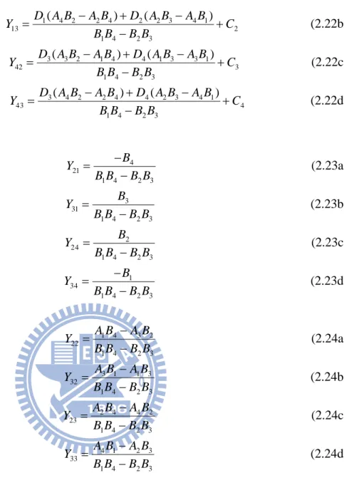
1 2 2 1 14 1 4 2 3 B D B D Y B B B B (2.21b) 4 3 3 4 41 1 4 2 3 B D B D Y B B B B (2.21c) 2 3 1 4 44 1 4 2 3 B D B D Y B B B B (2.21d) 1 3 2 1 4 2 1 3 3 1 12 1 1 4 2 3 ( ) ( ) D A B A B D A B A B Y C B B B B (2.22a)
1 4 2 2 4 2 2 3 4 1 13 2 1 4 2 3 ( ) ( ) D A B A B D A B A B Y C B B B B (2.22b) 3 3 2 1 4 4 1 3 3 1 42 3 1 4 2 3 ( ) ( ) D A B A B D A B A B Y C B B B B (2.22c) 3 4 2 2 4 4 2 3 4 1 43 4 1 4 2 3 ( ) ( ) D A B A B D A B A B Y C B B B B (2.22d) 4 21 1 4 2 3 B Y B B B B (2.23a) 3 31 1 4 2 3 B Y B B B B (2.23b) 2 24 1 4 2 3 B Y B B B B (2.23c) 1 34 1 4 2 3 B Y B B B B (2.23d) 1 4 3 2 22 1 4 2 3 A B A B Y B B B B (2.24a) 3 1 1 3 32 1 4 2 3 A B A B Y B B B B (2.24b) 2 4 4 2 23 1 4 2 3 A B A B Y B B B B (2.24c) 4 1 2 3 33 1 4 2 3 A B A B Y B B B B (2.24d) 2.2.3 Bandwidth Calculation
Figure 2.5 shows a four-port coupler with arms of arbitrary lengths, arbitrary characteristic impedances and arbitrary terminations. Analysis of the crossover coupler in Figure 2.2 can be formulated by the block ABCD matrices. To find the entries of the block
ABCD matrix, the Y-parameters of a four-port coupler in Figure 2.5 are derived first. By
definition, Y11 = I1/V1 when port 2, 3 and 4 are short-circuited. Based on the input admittance of a loaded transmission line, the result is shown in (2.25a). All other entries in the Y-matrix can be obtained in a similar fashion, and the results are in (2.25b) to (2.25i).
11 1cot 1 2cot 2 Y jY
jY
(2.25a) 22 1cot 1 3cot 3 Y jY
jY
(2.25b) 33 3cot 3 4cot 4 Y jY
jY
(2.25c) 44 2cot 2 4cot 4 Y jY
jY
(2.25d) Y12 Y21 jY1csc
1 (2.25e) 14 41 2csc 2 Y Y jY
(2.25f) 23 32 3csc 3 Y Y jY
(2.25g) 34 43 4csc 4 Y Y jY
(2.25h) 13 31 24 42 0 Y Y Y Y (2.25i)These Y-parameters are then transformed into four-port block ABCD parameters as shown in section 2.2.2. Multiplying the ABCD matrices of each stage, the total ABCD matrix of the crossover in Figure 2.2 can be obtained. The overall S-parameter matrix can be calculated when the total ABCD matrix is transformed into Y matrix which is then transformed into the
S-matrix. If a 20-dB return loss, 0.5-dB insertion loss and 20-dB isolation are referred, the
bandwidth of the crossover coupler can be obtained by computation using a computer program.
The proposed crossover coupler in Figure 2.2 has four design parameters Zo1, Zo2, Zi =
Zi1 = Zi2 and When the above parameters are determined, the impedances of the arms Z1~Z7 can be obtained from (2.3) and (2.4). Z01, Z02 and Zi are fixed and S-parameters are measured when port 1 and port 3 are terminated in Z01 and port 2 and port 4 are terminated in Z02. The
values of Z01 and Z02 will not affect the S-parameters but the ratio of Z01 to Z02 does, because
Z1~Z7 will maintain the same ratio when the ratio of Z01 to Z02 is fixed. Then power division ratio is swept, and the bandwidth is calculated. The relation between and the calculated bandwidth are discussed as follows.
Figure 2.6 shows the calculated bandwidth for Zi1 = Zi2 = Z01. Each S-parameter may have its own response and bandwidth. Figure 2.6 (a) shows the bandwidth of |S11| and |S33|, Figure 2.6 (b) shows those of |S12| and |S34|, Figure 2.6 (c) shows those of |S13| and |S24|, Figure 2.6 (d) shows those of |S14| and |S23|, and Figure 2.6 (e) shows those of |S22| and |S44|. The other
S-parameters can be known by the reciprocity theorem. In each port, curve 1 uses Z01:Z02 = 1:1, curve 2 uses Z01:Z02 = 1:2, curve 3 uses Z01:Z02 = 1:4, curve 4 uses Z01:Z02 = 2:1 and curve 5 uses Z01:Z02 = 4:1. When = 45o, the circuit has the best matching condition for all termination impedance ratios, while the circuit has the best isolation when the power coefficient is 20o or 70o. In Figure 2.7 and Figure 2.8, Zi1 and Zi2 are replaced by Z02 and Z Z01 02 , respectively. The trend of the circuit bandwidths of the S-parameters is similar to those in Figure 2.7.
3
2
4
1
02Y
Y
03 04Y
Y
01Y ,
4
3Y ,
Y ,
2
1Y ,
4 3 2 10
3
6
9
12
15
18
21
24
bandwidth of S and S
(%)
20
30
40
50
60 70 20 30
40
50
60
70
11 33
(a)12
15
18
21
24
bandwidth of S and S
(%
)
20
30
40
50
60 70 20 30
40
50
60
70
12 34
(b)4
6
8
10
12
14
16
18
20
bandwidth of S and S
(%)
20
30
40
50
60 70 20 30
40
50
60
70
13 24
(c)3.5
4
4.5
5
5.5
6
6.5
7
7.5
bandwidth of S
and S
(%
)
20
30
40
50
60 70 20 30
40
50
60
70
14 23
(d)0
25
50
75
100
bandwidth of S
and S
(%)
20
30
40
50
60 70 20 30
40
50
60
70
22 44
(e)Figure 2.6 Bandwidths measured by S-parameter responses. Port 1 and port 3 are terminated in Z01 and port 2 and port 4 are terminated in Z02. Zi1 = Zi2 = Z01. Curves 1 ~ 5 have Z01:Z02 = 1:1, 1:2, 1:4, 2:1, and 4:1, respectively. (a) |S11| and |S33|. (b) |S21| and |S34|. (c) |S13| and |S24|. (d) |S14| and |S23|. (e) |S22| and |S44|.
0
25
50
75
100
bandwidth of S and S
(%)
20
30
40
50
60 70 20 30
40
50
60
70
11 33
(a)12
15
18
21
24
bandwidth of S and S
(%)
20
30
40
50
60 70 20 30
40
50
60
70
12 34
(b)4
6
8
10
12
14
16
18
20
bandwidth of S and S
(%)
20
30
40
50
60 70 20 30
40
50
60
70
13 24
(c)3.5
4
4.5
5
5.5
6
6.5
7
7.5
bandwidth of S and S
(%)
20
30
40
50
60 70 20 30
40
50
60
70
14 23
(d)0
3
6
9
12
15
18
21
24
bandwidth of S and S
(%)
20
30
40
50
60 70 20 30
40
50
60
70
22 44
(e)Figure 2.7 Bandwidths measured by S-parameter responses. Port 1 and port 3 are terminated in Z01 and port 2 and port 4 are terminated in Z02. Zi1 = Zi2 = Z02. Curves 1 ~ 5 have Z01:Z02 = 1:1, 1:2, 1:4, 2:1, and 4:1, respectively. (a) |S11| and |S33|. (b) |S21| and |S34|. (c) |S13| and |S24|. (d) |S14| and |S23|. (e) |S22| and |S44|.
0
5
10
15
20
25
30
35
40
bandwidth of S and S
(%)
20
30
40
50
60 70 20 30
40
50
60
70
11 33
(a)14
15
16
17
18
19
20
21
22
bandwidth of S and S
(%)
20
30
40
50
60 70 20 30
40
50
60
70
12 34
(b)5
8
11
14
17
bandwidth of S and S
(%)
20
30
40
50
60 70 20 30
40
50
60
70
13 24
(c)5
5.3
5.6
5.9
6.2
bandwidth of S and S
(%)
20
30
40
50
60 70 20 30
40
50
60
70
14 23
(d)0
5
10
15
20
25
30
35
40
bandwidth of S and S
(%)
20
30
40
50
60 70 20 30
40
50
60
70
22 44
(d)Figure 2.8 Bandwidths measured by S-parameter responses. Port 1 and port 3 are terminated in Z01 and port 2 and port 4 are terminated in Z02. Zi1 = Zi2 = Z Z01 02 . Curves 1 ~ 5 have
Z01:Z02 = 1:1, 1:2, 1:4, 2:1, and 4:1, respectively. (a) |S11| and |S33|. (b) |S21| and |S34|. (c) |S13| and |S24|. (d) |S14| and |S23|. (e) |S22| and |S44|.
2.3 Simulation and Measurement
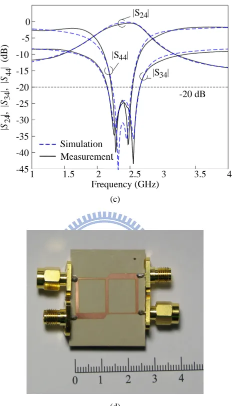
Two circuits are fabricated and measured to validate the design. Figure 2.9 (a) ~ (c) plot the simulation and measurement of the first fabricated circuit with Zo1 = 25 , Zo2 = 100 , Zi = 100 and 46
. The center frequency is designed at 2.45 GHz. The circuit simulation is done by the software package IE3D [20]. The substrate has r = 10.2 and h = 1.27 mm. The
S-parameters are measured with reference port impedance 50 . The measured data are
converted to S-parameters with designated port impedances with the aids of Y-parameters. If a 20-dB return loss, 0.5dB insertion loss and 20-dB isolation are referred, the estimation bandwidths are shown as curve 3 of Figure 2.7. The estimated bandwidths of |S11|, |S21|, |S31|, |S41|, |S22|, |S23|, |S24|, |S33|, |S34| and |S44| are 92.9%, 16.5%, 13.4%, 4.1%, 10.3%, 4.1%, 12.2%, 23.4%, 16.3% and 10.4%. Figure 2.9 (a)~(c) show the simulation IE3D bandwidths of |S11|, |S21|, |S31|, |S41|, |S22|, |S23|, |S24|, |S33|, |S34| and |S44| are 92%, 21%, 13.3%, 4.3%, 12.1%, 4.4%, 10.2%, 32.5%, 20.7% and 12.1% and the measured responses have 85.7%, 20.5%, 10.4%, 4.9%, 14.4%, 4.3%, 3.7%, 62.4%, 20.5% and 13.1% respectively. The measured data has good agreement with the simulation and the calculation. Figure 2.9 (d) shows the photo of the experimental circuit.
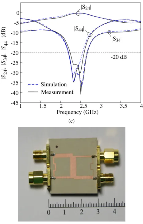
Figure 2.10 (a) ~ (c) plot the simulation and measurement results of the second fabricated circuit with Zo1 = 100 , Zo2 = 50 , Zi = 50 and 40. Again, a 20-dB return loss, 0.5dB insertion loss and 20-dB isolation are referred, and the estimation bandwidths are shown as curve 4 in Figure 2.6. The calculated bandwidths of |S11|, |S21|, |S31|, |S41|, |S22|, |S23|, |S24|, |S33|, |S34| and |S44| are 9.48%, 17.5%, 14.8%, 5.8%, 15.36%, 5.74%, 16.73%, 9.98%, 16.87% and 12.9%, respectively. Figure 2.10 (a)~(c) show the simulation bandwidths of |S11|, |S21|, |S31|, |S41|, |S22|, |S23|, |S24|, |S33|, |S34| and |S44| are 10.36%, 19.12%, 12.86%, 5.79%, 18.06%, 5.73%, 15.25%, 11.09%, 18.72% and 14.53% and the measured results have 11.63%, 19.59%, 6.43%, 5.51%, 15.31%, 6.12%, 11.94%, 14.39%, 18.98% and 14.08%, respectively.
The measured responses have good agreement with the simulation and calculation. Figure 2.10 (d) shows the photo of the realized circuit.
0 11 12 |S |, | S |, | S |, | S | (dB) 1 1.5 2 2.5 3 3.5 4 Frequency (GHz) -5 -10 -15 -20 -25 -30 -35 -40 -45 13 14 Simulation Measurement -20 dB |S |13 |S |14 |S |12 |S |11 (a) 0 1 1.5 2 2.5 3 3.5 4 Frequency (GHz) -5 -10 -15 -20 -25 -30 -35 -40 -45 22 23 |S | , | S |, | S | (dB) 33 -20 dB |S |23 |S |22 |S |33 Simulation Measuremen
t
(b)0 1 1.5 2 2.5 3 3.5 4 Frequency (GHz) -5 -10 -15 -20 -25 -30 -35 -40 -45 24 34 |S |, | S |, | S | (dB) 44 |S |24 |S |44 |S |34 -20 dB Simulation Measurement (c) (d)
Figure 2.9 The S-parameters of the first fabricated circuit with Zo1 = 25 , Zo2 = 100 , Zi = 100 and 46. (a) |S
11|, |S21|, |S31|, |S41|. (b) |S22|, |S23, |S33|. (c) |S24|, |S34|, |S44|. (d) The circuit photo. W1 ~ W7 are 2.06, 0.48, 1.01, 1.1, 1.18, 0.43 and 2.19 mm. L1 ~ L7 are 11.06, 11.69, 11.42, 11.39, 11.35, 11.72 and 11.02 mm.
0 11 12 |S |, | S |, | S |, | S | (dB) 1 1.5 2 2.5 3 3.5 4 Frequency (GHz) -5 -10 -15 -20 -25 -30 -35 -40 -45 13 14 Simulation Measurement |S |13 |S | 11 |S |14 |S |12 -20 dB (a) 0 1 1.5 2 2.5 3 3.5 4 Frequency (GHz) -5 -10 -15 -20 -25 -30 -35 -40 -45 22 23 |S |, | S |, | S | (dB) 33 Simulation Measurement |S |22 |S |23 |S |33 (b)
0 1 1.5 2 2.5 3 3.5 4 Frequency (GHz) -5 -10 -15 -20 -25 -30 -35 -40 -45 24 34 |S |, | S |, | S | (dB) 44 -20 dB Simulation Measuremen
t
|S |24 |S |44 |S |34 (c) (d)Figure 2.10 The S-parameters of the second fabricated circuit with Zo1 = 100 , Zo2 = 50 , Zi = 50 and 40
. (a) |S11|, |S21|, |S31|, |S41|. (b) |S22|, |S23, |S33|. (c) |S24|, |S34|, |S44|. (d) Circuit photo. W1 ~ W7 are 1.33, 1.84, 0.74, 3.74, 0.26, 2.49 and 0.92 mm. L1 ~ L7 are 11.29, 11.12, 11.55, 10.7, 11.85, 10.95 and 11.47 mm.
Chapter 3
Dual-Band Crossover Coupler Design
Recent rapid progress in wireless communications has created a need of dual-band operation for RF devices, such as the global systems for mobile communication systems (GSM) at 0.9/1.8 GHz and wireless local area network (WLAN) at 2.4/5.2 GHz. This Chapter studies the design of crossover coupler with dual-band operation.
3.1 Elementary Two-Port for Dual-Band Operation
Figure 3.1 shows the elementary two-port for substituting a /4-section to achieve dual-band operation. The elementary two-port consists of two high-Z sections on both sides with two stubs being attached to their ends and a low-Z section in the middle. Let the admittance of the two shunt stubs be jB/2. Since the circuit is symmetric about its center, by setting the reference plane in the middle open- and short-circuited, respectively, the input admittances for even- and odd-mode, ye = y11 + y21 and yo = y11 -
y21, can be readily derived as follows:
2 1 11 21 1 1 2 tan tan 1 2 1 tan tan s s s s R B y y j j Z R (3.1a) 2 1 11 21 1 1 2 cot tan 1 2 1 tan cot s s s s R B y y j j Z R (3.1b)
Let the two designated operation frequencies be f1 and f2 = nf1. To have the crossover junction operate with a dual-passband characteristic, each /4-section of the two asymmetric branch-line hybrids is replaced by the elementary two-port network, which is capable of providing 90 and 270 degrees at f1 and f2, respectively. The following equations can be derived.
21( )1 ( ( s1, s2) ( s1, s2)) / 2 s1/ T y f P Q Z Z (3.2a) 21( 1) ( ( s1, s2) ( s1, s2)) / 2 s1/ T y nf P Q Z Z (3.2b) 1 ( )1 ( ( 1, 2) ( 1, 2)) s s s s s Z B f P Q (3.2c) 1 ( 1) ( ( 1, 2) ( 1, 2)) s s s s s Z B nf P Q (3.2d) where tan tan ( , ) 1 tan tan R P R (3.3a) tan cot ( , ) 1 tan cot R Q R (3.3b)
where R = Zs1/Zs2, ZT can be the characteristic impedance of the /4-section, and B/2 is
the susceptance of the shunt open stub. y21(f1) = Im[Y21(f1) Z1] and y21(nf1) = Im[Y21(nf1) Z1] represent respectively the normalized (2, 1) entry of the Y-matrix of the two-port at f1 and f2 = nf1. Fig. 3.2(a) and (b) plot both y21(f1) and y21(nf1) curves against s1 for various R values when s2 = 5o and 10o, respectively. Both s1 and s2 are
evaluated at f1. For each R, the intersection point of the y21(f1) and y21(nf1) curves gives the solution. Inserting these solutions into (3.2c) and (3.2d), values of B(f1) and B(nf1), and hence the electrical length and characteristic impedance of open stubs, can be obtained.
Z
s1
s1
s1Z
s1
s2Z
s2
s2
t1
t1Z
t1Z
t1Figure 3.1 Two-port network for subsituting a quarter-wave section.
0
5
10
15
20
25
30
0
(degree)
y
21(
)
R=4
R=2
R=1
s1y
21(nf )
1(f )
y
21 11
2
3
4
5
(a)0
5
10
15
20
25
30
(degree)
s1R=4
R=2
R=1
y
21(nf )
1(f )
y
21 10
y
21(
)
1
2
3
5
4
(b)Figure 3.2 Design graphs for determining s1 and R. (a) s2 = 5o. (b) s2 = 10o. Both s1
and s2 values are referred to f1.
3.2 Simulation and Measurement
A microstrip crossover coupler designed at 0.9/1.8 GHz is fabricated and measured for demonstration. The circuit is built on a substrate of r = 10.2 and h = 0.508 mm. The
characteristic impedances of the branches in Figure 3.3 are Za1 = 39.36 , Zb1 = 33.17 ,
Za2 = 29.67 , Za3//Zb2 = 36.93 , Zb3 = 42.13 , Za4 = 27.83 , and Zb4 = 46.91 .
Termination impedances of the port 1 and port 3 are Zo1 and these of the port 2 and port
4 are Zo2. Each branch is subsituted by the two-port in Fig. 3.1 by using the solutions in
Fig. 3.2(b) with R = 2, s1 = 15o and s2 = 10o.
Figure 3.4 compares the measured results with the simulation data obtained by the IE3D [18]. Figure 3.4(a) and 3.4(b) plots the circuit responses when port 1 is excited, and 3.4(c) and 3.4(d) draws the results when signal is fed to port 2. In Fig. 3.4(a), it can
be observed that the measured return losses |S11| and the isolations |S41| at the two designated frequencies are better than -20 dB. If a 15-dB return loss is referred, measured data indicate that |S11| has bandwidths of 10.8% and 4.6% and |S11| has 3.5% and 4.2% at f1 and f2, respectively. Fig. 3.4(b) shows the isolation between port 2 and port 1 |S21| and the crossover response |S31|. The measured |S31| = –0.89 dB and –1.1 dB at f1 and f2, respectively. When input is at port 2, the measured return loss |S22| in Fig. 3.4(c) is better than -20 dB and has bandwidths of 15% and 5.8% at f1 and f2, respectively, for a 15-dB reference. The experimental |S32| indicate that the isolations between ports 2 and 3 are better than 20 dB in both bands. In Fig. 3.4(d), the measured |S42| = –0.69 dB and –1.24 dB at f1 and f2, respectively. In Fig. 3.4(a) through 3.4(d), reasonably good agreement between the simulation and measurement can be observed. Fig. 3.4(e) shows the photograph of the experimental four-port dual-band crossover junction.
3
2
4
1
Z
i2 i1Z
Z
b2 o2Z
Z
o1 o2Z
Z
o1Z
a4Z
b4Z
b3 a3Z
Z
a2Z
b1 a1Z
Figure 3.3 Two cascaded asymmetric branch-line hybrids to form a new crossover coupler with arbitrary diagonal port impedances Zo1 and Zo2.
0.5
0.75
1.0
1.25
1.5
1.75
2.0
-50
-40
-30
-20
-10
0
Frequency (GHz)
11 41|S
|, |
S
| (dB)
-15 dB
11|S |
41|S |
Simulation
Measuremen
t
(a)0.5
0.75
1.0
1.25
1.5
1.75
2.0
-50
-40
-30
-20
-10
0
Frequency (GHz)
21 31|S
|, |
S
| (dB)
-15 dB
31|S |
21|S |
Simulation
Measuremen
t
(b)0.5
0.75
1.0
1.25
1.5
1.75
2.0
-50
-40
-30
-20
-10
0
Frequency (GHz)
22 32|S
|, |
S
| (dB)
-15 dB
22|S |
32|S |
Simulation
Measuremen
t
(c)0.5
0.75
1.0
1.25
1.5
1.75
2.0
-50
-40
-30
-20
-10
0
Frequency (GHz)
12 42|S
|, |
S
| (dB)
-15 dB
42|S |
12|S |
Simulation
Measuremen
t
(d)(e)
Figure 3.4 Simulation and measured responses of the fabricated dual-band crossover junction. (a) |S11| and |S41|. (b) |S21| and |S31|. (c) |S22| and |S32|. (d) |S12| and |S42|. Zo1 = 50
Chapter 4
Conclusion
A new design for crossover coupler with different diagonal port impedances is devised by using a cascade of asymmetric branch-line couplers with arbitrary power division. It allows the port termination impedances to be arbitrary. Circuit analysis in term of block
ABCD matrix and Y-matrix formulation is used to calculate the bandwidth associated with
each S-parameter. In the second part of this thesis, the crossover is devised to have dual-band operation. Each quarter-wave section is replaced by an elementary two-port shown which is designed to achieve proper phase changes at the two designated frequencies. One microstrip circuit for operation at 0.9/1.8 GHz is realized. The measured responses not only validate the idea but also agree well with the simulation.
There is still some room for improving the performance of the proposed crossover couplers. First, is it possible to synthesize a passband of crossover couplers like a filter? The passband function can be maximally flat response, Butterworth response or elliptic function response. Furthermore, the size of a microstrip realization can be too large to be used in some applications. It needs miniaturizing circuit size and keeping the flexibility of the port termination impedances at the same time. Second, if a passband response can be synthesized for a crossover coupler, many existing design techniques for dual-band bandpass filter can be useful for microwave passive circuit.
References
[1] T.-S. Hong, “A rigorous study of microstrip crossovers and their possible improvements,” IEEE Trans. Microw. Theory Tech., vol. 42, no. 9, pp. 1802-1806, Sep.
1994.
[2] C.-C. Chang, T.-Y. Chin, J.-C. Wu and S.-F. Chang, “Novel design of a 2.5-GHz fully integrated CMOS Butler matrix for smart-antenna systems,” IEEE Trans. Microw.
Theory Tech., vol. 56, no. 8, pp. 1757 - 1763, Aug. 2008.
[3] J. S. Wight, W. J. Chudobiak and V. Makios, “A microstrip and stripline crossover structure,” IEEE Trans. Microw. Theory Tech., vol. 24, no. 5, pp. 270, May 1976.
[4] F. C. de Ronde, “Octave-wide matched symmetrical, reciprocal, 4- and 5 ports,” in
IEEE MTT-S Int. Microw. Symp. Dig., pp. 521–523, Jun.1982.
[5] K. C. Gupta and M. D. Abouzahra, “Analysis and design of four-port and five-port microstrip disk circuits,” IEEE Trans. Microw. Theory Tech., vol. 33, no. 12, pp. 1422-1428, Dec. 1985.
[6] D. V. Kholodniok and I. Vendik, “A novel type of 0-dB directional coupler for microwave integrated circuits,” in 29th European Microw. Conf., pp. 341-344, Nov. 1999.
[7] D. V. Kholodniok, G. Kalinin, E. Vernoslova, and I. Vendik, “Wideband 0-dB branch-line directional couplers,” in IEEE MTT-S Int. Microw. Symp. Dig., pp. 1307–1310, Jun. 2000.
[8] Y. Chen and S.-P. Yeo, “A symmetrical four-port microstrip coupler for crossover application,” IEEE Trans. Microw. Theory Tech., vol. 55, no. 11, pp. 2434-2438, Nov. 2007.
[9] Y.-C. Chiou, C.-H. Tsai and J.-T. Kuo, “Comments on “A symmetrical four-port microstrip coupler for crossover application,” ” IEEE Trans. Microw. Theory Tech., vol. 57, no. 7, pp. 1859-1860, July. 2009.
[10] Y.-C. Chiou, J.-T. Kuo and H.-R. Lee, “Design of compact symmetric four-port crossover junction,” IEEE Microw. Wireless Component Letters, vol. 19, no. 9, pp. 545-547, September 2009.
[11] H.-R. Ahn, I. Wolff and I.-S. Chang, “Arbitrary termination impedances, arbitrary power division, and small-sized ring hybrids,” IEEE Trans. Microw. Theory Tech., vol. 45, no. 12, pp. 2241-2247, Dec. 1997.
[12] H.-R. Ahn and I. Wolff, “Asymmetric four-port and branch-line hybrids,” IEEE Trans.
Microw. Theory Tech., vol. 48, no. 9, pp. 1585-1588, Sep. 2000.
[13] J.-T. Kuo, T.-H. Yeh and C.-C. Yeh, “Design of microstrip bandpass filters with a dual-passband response,” IEEE Trans. Microwave Theory Tech., vol. MTT-53, no. 4, pp. 1331-1337, Apr. 2005.
[14] K.-K. M. Cheng and F.-L. Wong, “A novel approach to the design and implementation of dual-band compact planar 90° branch-line coupler,” IEEE Trans. Microw. Theory Tech., vol. 52, no. 11, pp. 2458-2463, Nov. 2004.
[15] C.-L. Hsu, J.-T. Kuo and C.-W. Chang, “Miniaturized dual-band hybrid couplers with two arbitrary power division ratios,” IEEE Trans. Microwave Theory Tech., vol. MTT-57, no. 1, pp. 149-156, Jan. 2009.
[16] I.-H. Lin, M. Devincentis, C. Caloz and T. Itoh, “Arbitrary dual-band components using composite right/left-handed transmis-sion lines,” IEEE Trans. Microw. Theory Tech., vol. 52, no.4, pp. 1142-1149, Apr. 2004.
[17] C. Monzon, “A small dual-frequency transformer in two sections,” IEEE Trans. Microw.
Theory Tech., vol. 51, no. 4, pp. 1157-1161, Apr. 2003.
[18] S. Srisathit, M. Chongcheawchamnan, and A. Worapishet, “Design and realization of dual-band 3 dB power divider based on two-section transmission-line topology,” IEE
Electronics Lett., vol. 39, no. 9, pp. 723-724, May 2003.
[19] Yu-Shin Wang, Ming-Chou Lee, and Shyh-Jong Chung, “Two PIFA-Related Miniaturized Dual-Band Antennas,” IEEE Trans. Antennas Progagat., Vol. 55, No. 3, Mar. 2007