The Processing Windows for Selective Copper
Chemical Vapor Deposition from
Cu(hexafluoroacetylacetonate)
trimethylvinylsilane
Jung-Chao Chiou, Kuen-Chi Juang, and Mao-Chieh Chen*
Department of Electronics Engineering and the Institute of Electronics, National Chiao-Tung University, Hsinchu, Taiwan
A B S T R A C T
T o identify the processing tolerance for the selective C u c h e m i c a l v a p o r deposition (Cu C V D ) the processing w i n d o w s w e r e constructed w i t h respect to deposition pressure a n d substrate t e m p e r a t u r e over thermally g r o w n SiO2 v s . various conducting substrates of W, CoSif, TiN, TiW, a n d A1. It is found that the width of selective deposition window decreases as the deposition pressure is increased, a n d no selective Cu deposition can be obtained as the deposition pressure exceeds 120 mTorr. The lowest temperatures for Cu CVD on various SiO2 substrates including thermally grown, BPSG, TEOS, a n d PECVD SiO2 were determined so that processing windows for selective Cu deposition on variously patterned wafers can be constructed. The selective Cu deposition was also conducted on p a t t e r n e d substrates with submicrometer feature sizes using the PECVD SiO2 as the interlayer dielectric. The n u c l e a t i o n of Cu on the SiO2 surface obviously acts as the major l i m i t a t i o n for achieving selective Cu CVD. We postulate that the Cu c o n t a i n i n g adspecies, Cu(hfac), on the insulating SiO2 surface m a y combine by surface diffusion, a n d these assembled adspecies then disproportionate by exchanging electrons with each other rather t h a n transferring electrons through the substrate.
Selective copper chemical vapor deposition (Cu CVD) has been regarded as a potential metallization process in deep submicrometer integrated circuit applications, n o t
only because it deposits Cu films with low resistivity a n d high electromigration resistance b u t also because it offers a superior ability for via hole filling of high aspect ratio. I-4 In addition, the selective C u deposition does not n e e d a subse- q u e n t etching process, w h i c h is a m a j o r processing obstacle for a p p l y i n g C u as interconnection material. ~-6 M o s t of the selective C u C V D w a s c o n d u c t e d b y using the Cu(R)2, ab- breviated as Cu(II), a n d C u ( R ) L , abbreviated as Cu(I), se- ries precursors, w h e r e R is a ~-diketonate ligand a n d L is a L e w i s base. 7-~I T h e C u ( R ) L precursor has attracted m u c h attention in recent years b e c a u s e of its relatively l o w d e p o - sition t e m p e r a t u r e a n d H 2 is not required as a reducing gas. T h e Cu(I) precursor is usually available in liquid f o r m a n d delivered b y the carrier gas, allowing accurate control of the gas flux. M a n y Cu(I) precursors h a v e p r o v e d to be capa- ble of depositing C u film w i t h l o w resistivity a n d s o m e of these precursors h a v e also exhibited the selective deposi- tion behavior. 12-I~ It has b e e n reported that Cu(I) series c o m p o u n d s deposit C u b y a disproportionation reaction that n e e d s electron transfer b e t w e e n t w o Cu(R) adspecies. 16 Therefore, the selectivity o n c o n d u c t i n g v s . insulating sur- faces should be existent according to the electron transfer process.
T h e selective C u c h e m i c a l v a p o r deposition, however, w a s f o u n d to be a c o m p l e x process. T h e conductivity of the substrate is just one of the p a r a m e t e r s that determines se- lective deposition. Substrate temperature, reaction pres- sure, a n d surface treatment of the substrate all h a v e pro- f o u n d effects o n achieving the selective deposition. ~7 A s the selective deposition is achieved b y controlling the relative g r o w t h rate of C u o n the c o n d u c t o r a n d insulator substrate surfaces, a n y factor that influences the g r o w t h b e h a v i o r of C u needs to b e carefully e x a m i n e d a n d well controlled; then, the selective C u C V D can b e possibly successful.
This w o r k gives a detailed study o n selective C u C V D using C u ( h f a c ) T M V S as the precursor, w h e r e hfac repre- sents l,l,l,5,5,5-hexafluoroacetylacetonate a n d T M V S is trimethylvinylsilane. A s o n e of the m o s t p r o m i s i n g pre- cursors for selective C u C V D , C u ( h f a c ) T M V S has b e e n ex- tensively studied a n d verified to be capable of c o n d u c t i n g selective C u film deposition at relatively l o w t e m p e r a - tures. ~'~9 T h e r e are m a n y reports of selective C u C V D f r o m C u ( h f a c ) T M V S ; ~2'17'2~ however, selectivity loss w a s fre- quently observed. T h e controversy m a y result f r o m the dis-
* Electrochemical Society Active Member.
J. Electrochem. Soc., Vol. 142, No. 1, January 1995 9 The
c r e p a n c y of the processing apparatus, the w i d e l y c h o s e n e x p e r i m e n t a l parameters, a n d the varieties of s a m p l e preparation. In addition, the c h e m i c a l species a n d the p h o - toresist that r e m a i n s o n the SiO2 surface after the processes for pattern generation w e r e also considered to b e responsi- ble for the selective loss. ~8 A detailed investigation o n the selective w i n d o w s as a function of processing p a r a m e t e r s will be helpful in finding the o p t i m u m processing condi- tions for selective deposition of copper.
B e c a u s e selective C u C V D is sensitive to the impurities
o n the substrate surface, selective C u deposition w a s first p e r f o r m e d o n the u n p a t t e r n e d substrates to d e t e r m i n e the possible selective processing w i n d o w s for t e m p e r a t u r e a n d pressure. Next, the deposition w a s carried out o n patterned substrates to further investigate the effects of patterning o n
the selectivity w i n d o w a n d to d e t e r m i n e process imple- m e n t a t i o n for C u film deposition. T h e activation energies of C u C V D o n various substrates w e r e calculated f r o m the A r r h e n i u s plot of deposition rate v s . temperature. T h e i m - purity a n d resistivity of the C u films w e r e m e a s u r e d a n d analyzed. T h e effects of processing p a r a m e t e r s o n selective C u C V D w e r e investigated. Finally, discussion w a s m a d e o n
m e c h a n i s m of selective C u deposition.
Experimental Procedure
Selective Cu deposition from Cu(hfac)TMVS was per- formed on conducting a n d i n s u l a t i n g as well as patterned a n d u n p a t t e r n e d substrates. The i n s u l a t i n g substrates in- cluded the thermally grown S i Q , borophosphosilicate glass (BPSG), tetraethyl orthosilicate (TEOS) deposited SiOf, and the plasma enhanced chemical vapor deposited (PECVD) S i Q , while the conducting substrates included W, TiN, TiW, and A] layers deposited on thermally oxidized Si wafers, a n d a CoSt2 layer grown on Si substrate. The layers of W a n d A1 were deposited using a n E - b e a m evaporation system, while the layer of TiW was sputter deposited from a TiW target [Ti 10 weight percent (w/o)]. The TiN film was formed by reactively sputtering a Ti target (99.99%) using a mixed gas of Ar + N2 (5:1). The CoSt2 substrate was con- structed by thermally a n n e a l i n g an c~Si(50 A)/Co(200 -~)/Si structure at 550~ for 90 rain. 22
The p a t t e r n e d substrates contain via holes a n d fine lines with submicrometer feature sizes. The patterned samples were fabricated on 6 in. diam Si wafers as follows. After an SiO2 layer was thermally grown, the conducting layer, such as A1, was deposited. This was followed by a deposition of 5000 A of PECVD SiOf. Finally, patterns were defined on the PECVD S i Q layer by standard photolithographic techniques.
w e r e cooled in A r a m b i e n t at a pressure of i0 Torr. A s c a n n i n g electron m i c r o s c o p e ( S E M ) w a s u s e d to ob- serve the surface m o r p h o l o g y of the C u films. T h e sheet resistance of the C u films w a s m e a s u r e d b y a four-point probe, a n d the film thickness w a s m e a s u r e d b y a D e k - T e k surface profiler a n d also d o u b l e c h e c k e d b y S E M cross-sec- tional m e a s u r e m e n t . A u g e r electron spectroscopy ( A E S ) a n d s e c o n d a r y ion m a s s spectrometry ( S I M S ) w e r e e m - p l o y e d for i m p u r i t y analysis of the C u films.
Results and Discussion
Copper deposition on the unpatterned substrates.--The
C V D C u films w e r e deposited o n the u n p a t t e r n e d c o n d u c t - ing substrates of W, CoSi~, a n d A1 at various deposition t e m p e r a t u r e s a n d pressures for a source t e m p e r a t u r e of 4 0 ~ w i t h a n A r carrier gas flow of 20 s c c m a n d also for a source t e m p e r a t u r e of 60~ w i t h a n A r carrier gas flow of 40 sccm. Figure 1 s h o w s the A r r h e n i u s plots (deposition rate vs. temperature) for C u C V D o n the W substrate at a constant pressure of i0 m T o r r for t w o different conditions of source t e m p e r a t u r e a n d A r carrier gas flow rate. Activa- tion energy E~ of the C u C V D c a n be d e t e r m i n e d f r o m the slope of the linear s e g m e n t s of these A r r h e n i u s plots b y the e q u a t i o n K = A e x p ( - E J R T ) , w h e r e K is the deposition rate, R is the gas constant, a n d A is k n o w n as the A r r h e n i u s pre-exponential constant. T h e activation energy E~ is de- t e r m i n e d to b e 3.11 a n d 3.56 kcal/mol, respectively, at t e m - peratures a b o v e 2 0 0 ~ for the C V D condition of 60~ source t e m p e r a t u r e a n d 40 s c c m A r carrier gas flow a n d the C V D condition of 40~ source t e m p e r a t u r e a n d 20 s c c m A r car- rier gas flow; the c o r r e s p o n d i n g Ea values at t e m p e r a t u r e s b e l o w 2 0 0 ~ are d e t e r m i n e d to b e 20.0 a n d 13.4 kcal/mol. T h e l o w e r activation energy at t e m p e r a t u r e s a b o v e 2 0 0 ~ indicates that the C V D process b e c o m e s mass-transfer lim- ited at high t e m p e r a t u r e ) ~ T h e A r r h e n i u s plots for the C u deposition o n CoSiz a n d Al substrates are illustrated in Fig. 2 a n d Fig. 3, respectively. T h e activation energies for C u deposition o n CoSi~ a n d Al substrates are d e t e r m i n e d to
Z
o
9 c~ 280"C 240"C 201]'C 160"Clos
, , , ,102
101
0.0016
0.0018
0.0020
0.0022
TEMPERATURE(l/K)
0.0024
Fig. 1. Deposition rate v s . substrate temperature (Arrhenius plot)
for Cu CVD on W substrate at a constant pressure of 10 mTorr. The values of activation energy in units of kcal/mol are indicated in lhe illustration.
0.0016
0.0018
0.0020
0.0022
0.0024
TEMPERATURE ( 1/K )
Fig. 2. Depositan rate v s . substrate temperature (Arrhenius plot) for
Cu CVD on CoSi~ substrate at a constant pressure of 10 mTorr.
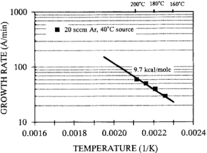
be 11.5 a n d 9.7 kcal/mol, respectively, for the C V D condi- tion of 40~ source t e m p e r a t u r e a n d 20 s c c m A r carrier gas flow. It w a s f o u n d that the C u film o n the CoSt2 a n d A1 substrates t e n d e d to peel off w h e n the substrate t e m p e r a - ture e x c e e d e d 220~ T h e peel-off of C u film f r o m the CoSiz a n d A l substrates m a y result f r o m the discrepancy of ther- m a l e x p a n s i o n coefficient b e t w e e n the C u film a n d the CoSt2 a n d Al layers. Figure 4 s h o w s the surface m o r p h o l o g y of C u films deposited at a pressure of i0 reTort for 20 rain, o n Al substrate at various temperatures. F o r the 20 rain deposition run, c o p p e r is still at the nucleation stage o n the 160~ A 1 substrate, while it has b e c o m e a continuous C u film o n the 170~ substrate. Substantial grain g r o w t h can be o b s e r v e d o n the C u film deposited o n the 2 0 0 ~ sub- strafe. Apparently, the C V D C u film is f o r m e d b y the nucle- ation a n d grain g r o w t h processes. Thus, once the C u is n u - cleated o n the substrate surface, it b e c o m e s C u g r o w n o n Cu. T h e surface m o r p h o l o g y of C V D C u film (Fig. 4) also revealed that the c o m p a c t C u grains f o r m e d a r o u g h sur- face, a n d the surface r o u g h n e s s increases w i t h the increase of film thickness a n d grain size. In addition, the surface often gets scratched during the D e k - T a k m e a s u r e m e n t s . Thus, the D e k - T a k m e a s u r e m e n t s w e r e carried out u n d e r the conditions of lightest pressure to avoid scratching. T h e l o w density a n d the r o u g h surface m a d e the thickness m e a s u r e m e n t difficult a n d m i g h t p r o d u c e s o m e error in de- termining the g r o w t h rate. T o r e d u c e this possible error, a S E M cross-sectional v i e w w a s e m p l o y e d to c h e c k the result of the thickness m e a s u r e m e n t , a n d a n average value of the thickness w a s t a k e n as the film thickness for a film w i t h a r o u g h surface. Therefore, the activation energy derived f r o m the A r r h e n i u s plot m a y be only a n a p p r o x i m a t e value.
200"C 180"C 160"C
1000 l ...
og
9,vkc .1(m~!%::.:.!:?.!!:.:.!!!:.!!:!!:
10
0.0016
0.0018
0.0020
0.0022
0.0024
TEMPERATURE (l/K)
Fig. 3. Deposition rate v s . substrate temperature (Arrhenius plot)
J. Electrochem. Soc.,
Vol. 142, No. 1, January 1995 9 The Electrochemical Society, Inc. 179Fig. 4. Surface morphology of Cu films deposited, at a pressure of 10 mTorr for 20 min, on AI sub- strafe at various substrate tem- perateres of (a) 160, (b) 170, (c) 180, and (d) 200~
T h e C u C V D o n the S i Q substrate is very different f r o m that o n the c o n d u c t i n g substrate. T h e m o s t m a r k e d differ- ence is the higher low-limit-temperature o n the SiO2 sub- strate. T h e low-limit-temperature is defined as the deposi- tion t e m p e r a t u r e b e l o w w h i c h n o C u nuclei c a n be discovered b y S E M observation (less t h a n 50 A) at a certain specified deposition condition. F o r e x a m p l e , the low-limit- t e m p e r a t u r e s at a pressure of 10 m T o r r are 160 a n d 140~ respectively, for W a n d T i W substrates, while the l o w - limit-temperature for the thermally g r o w n SiO2 substrate is 2 0 0 ~ at the s a m e deposition conditions. T h e processing w i n d o w of selective C u C V D is b a s e d o n the difference of low-limit-temperatures b e t w e e n the c o n d u c t i n g a n d S i Q substrates.
T h e selectivity w i n d o w s for the thermally g r o w n SiO2 v s . various c o n d u c t i n g substrates w i t h respect to the deposi- tion pressure a n d t e m p e r a t u r e are s u m m a r i z e d in Table I. T h e processing regions for the C u C V D o n Al a n d T i W sub- strates, as s h o w n in Fig. 5, are constructed f r o m the data listed in the table. F r o m Table I a n d Fig. 5, it is clear that as the deposition pressure is increased, low-limit-tempera- ture for b o t h c o n d u c t i n g a n d SiO2 substrates decreases, a n d also does the low-limit-temperature g a p b e t w e e n the c o n d u c t i n g a n d SiO2 substrates. A s a result, a triangular region for selective C u C V D is constructed for e a c h c o n d u c - tor-SiO2 pair. A s s h o w n in Fig. 5, blanket C u C V D c a n be carried out at high t e m p e r a t u r e a n d high pressure condi-
Table I. The processing windows for selective Cu CVD on thermally grown SiO2 vs. various conductive substrates.
1 0 m T o r r 5 0 m T o r r 1O0mTorr W(~ 160-200 140-160 130-140 CoSi2(~ 160-200 150-160 No selectivity TiN(~ 150-200 140-160 130-140 TiW(~ 140-200 130-160 130-140 AI(~ 150-200 140-160 No selectivity
tion, while selective C u C V D c a n be c o n d u c t e d w i t h the condition within the triangle region. F o r selective C u C V D in our system, the highest deposition pressure s h o u l d be limited to 100 a n d 120 mTorr, respectively, for the A1 a n d T i W substrates, a n d the c o r r e s p o n d i n g lowest t e m p e r a t u r e s h o u l d be limited to 140 a n d 130~ respectively.
In multilevel metallization system, C V D SiO2 layers are e m p l o y e d as the insulating dielectric; low-limit-tempera- ture of the C V D S i Q is l o w e r t h a n that of the thermally g r o w n SiO2 at a given deposition pressure. Table II lists the low-limit-temperatures for various SiO2 at three different deposition pressures. T h e r m a l l y g r o w n SiO2 apparently has the highest low-limit-temperature a m o n g the various ox- ides. Figure 6 s h o w s the processing w i n d o w s of selective C u C V D o n A l vs. thermally g r o w n S i Q a n d P E C V D SiO2. o LIJ 13/ C O C O rr LId 13_ 100 - -80 60 40 2C 100 ~ m a i l y Grown SiC
~
A[/Therrnally Grown SiONo n
Deposition
1:~o ~z,o 16o 18o
25o
220T E M P E R A T U R E (~
Fig. 5. The processing windows of selective Cu CVD on thermally grown SiO2 vs. AI and TiW substrates with respect to deposition
Nonetheless, the C u film deposition rate can be increased alternatively b y raising the source temperature a n d the carrier gas flowing rate, as s h o w n in Fig. 1 a n d Fig. 2. In addition, it is f o u n d that the deposition rate of C u increased b y increasing the source temperature (from 40 to 60~ a n d the carrier gas flow rate has little influence o n the selective w i n d o w .
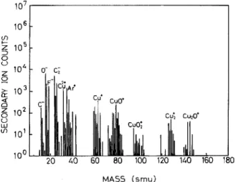
T h e m e a s u r e d resistivity of the C u film deposited in this w o r k lies in the range of 3-10 ~ - c m , w h i c h is a little higher than that of the b u l k material (1.67 ~ l - c m ) a n d that reported elsewhere. Iv'18 T h e impurities in the C u film are b e l o w the A u g e r detection limit; that is, the impurity levels are b e l o w 1 atomic percent (a/o) in the C u film. Figure 7 s h o w s the results of impurity analysis b y S I M S for the C u film deposited on the W substrate at 200~ Several h u n - dred A n g s t r o m s of the C u surface layer w e r e sputtered for r e m o v i n g the surface contamination before the S I M S anal- ysis. T h e F, O, a n d C w e r e f o u n d to be the m a j o r impurities within the C u film. T h e s e impurities m a y result f r o m in- c o m p l e t e desorption of the hfac ligand. It has b e e n f o u n d that the resistivity of the C u film can be correlated with the surface m o r p h o l o g y of the C u f i l m Y A s s h o w n in Fig. 4, the C V D C u film is c o m p o s e d of the c o m p a c t single grains a n d thus has a r o u g h surface. P o o r connection b e t w e e n the C u grains will lead to higher resistivity. Furthermore, m e a s - u r e m e n t b y four-point p r o b e o n a r o u g h surface tends to result in a higher value of sheet resistance.
Copper deposition on the patterned s u b s t r a t e s . - - T h e
CVD C u f i l m s w e r e d e p o s i t e d o n t h e p a t t e r n e d s u b s t r a t e s w i t h s u b m i c r o m e t e r f e a t u r e size to f u r t h e r i n v e s t i g a t e t h e s e l e c t i v e d e p o s i t i o n b e h a v i o r . F i g u r e 8(a) a n d (b) s h o w t h e s e l e c t i v e Cu CVD o n t h e A 1 / o x i d e p a t t e r n e d s u b s t r a t e s w i t h 20 s c c m A r c a r r i e r g a s f l o w a n d s o u r c e t e m p e r a t u r e s of 40 a n d 60~ r e s p e c t i v e l y . B o t h d e p o s i t i o n s w e r e c o n - d u c t e d f o r 20 m i n . T h e h i g h e r s o u r c e t e m p e r a t u r e s h o w s a s l i g h t l y i n c r e a s e d C u n u c l e a t i o n , b u t t h e s o u r c e t e m p e r a - t u r e b e t w e e n 40 a n d 60~ a p p a r e n t l y h a s l i t t l e i n f l u e n c e o n t h e s e l e c t i v e b e h a v i o r of C u CVD. D i f f e r e n t c o m b i n a t i o n s 100
[ ] At/Thermally Grown SiO 2 [ ] At t PECVD SiO 2 80 b ~ 60 uJ Blanket cr cO aJ 40 [3- 20 No Deposi t ion 120 140 - 160 180 2-00 220 TEMPERATURE (~
Fig. 6. The processing windows of selective Cu CVD on AI v s .
thermally grown SiO2 and PECVD SiO2 substrates with respect to deposition temperature and pressure for a 20 min deposition.
10 o
I
L Fl_/ iiii
20 40 60 80 100 120 140 160 180 M A S S ( s m u )
Fig. 7. The mass spectra of SIMS analysis for the Cu film deposited on W substrate at a temperature of 200~ and a pressure 10 mTorr. Cesium (Cs) was used as primary ion beam for the SIMS analysis.
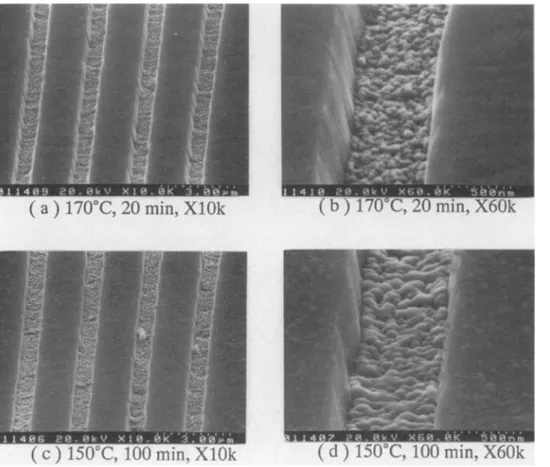
of deposition parameters within the selective deposition w i n d o w w o u l d p r o d u c e different results of the selective C u deposition. T h e S E M m i c r o g r a p h s s h o w n in Fig. 9 c o m p a r e the result of selective C u deposition c o n d u c t e d at i0 m T o r r a n d 170~ for 20 m i n with that c o n d u c t e d at I0 m T o r r a n d 150~ for 100 min. A l t h o u g h the deposition c o n d u c t e d at 150~ for i00 rain resulted in larger C u grains, it suffered f r o m selectivity loss. This is because the selective deposi- tion w i n d o w s h o w n in Fig. 6 is constructed b a s e d o n the data of the 20 m i n deposition run. T h e selective loss [Fig. 9(c) a n d 9(d)] obviously c a m e f r o m the nucleation of C u on the S i Q surface. Thus, it is preferable to conduct selective C u C V D at a higher temperature within the tolerance of the selective w i n d o w so as to shorten the deposition time a n d avoid the possible selectivity loss.
Mechanism of selectivity loss due to Cu nucleation on S i 0 2 . - - T h e s e l e c t i v e Cu CVD f r o m C u ( h f a c ) T M V S d e p e n d s o n a n u m b e r of d e p o s i t i o n p a r a m e t e r s as w e l l as s u b s t r a t e p r o p e r t i e s . T h e s u b s t r a t e t e m p e r a t u r e , d e p o s i t i o n p r e s s u r e , a n d s u r f a c e p r o p e r t i e s of s u b s t r a t e a l l h a v e p r o f o u n d ef- f e c t s on the selective deposition. I~'21'23 T h e selective C u C V D on metal/SiO2 substrate can be achieved b y controlling the deposition p a r a m e t e r s to p r o d u c e different C u nucleation a n d grain g r o w t h behavior o n the surface of conducting a n d S i Q substrates. Since the C u C V D proceeds with C u nucleation a n d grain g r o w t h procedures, successful selec- tive C u deposition d e p e n d s o n the appropriate control of C u nucleation a n d grain g r o w t h behavior. It is believed that C u C V D starts b y breaking the C u ( h f a c ) - T M V S b o n d (_--13 kcal/mol) a n d leaves a C u containing species, Cu(hfac), on the substrate surface to proceed with further dispropor- tionation reaction. 19'2~ F o r the cold-wall reaction system e m p l o y e d in this work, the source bath, delivery line, a n d the gas injector w e r e all kept at a temperature b e l o w 60~ to prevent the C u precursor f r o m d e c o m p o s i n g before the precursor reached the substrate surface. T h e energy for breaking the C u ( h f a c ) - T M V S b o n d is supplied f r o m the substrate heating. T h e molecular flux density c o n d e n s i n g on the substrate surface Ja (adsorption rate of molecular) can be expressed a s 25 Ja = nVa [1] w h e r e n = Po/kT is t h e n u m b e r of m o l e c u l e s p e r u n i t v o l - u m e , P0 is t h e m o l e c u l e p r e s s u r e , a n d va is t h e r o o t m e a n s q u a r e v e l o c i t y of m o l e c u l e i n t h e vapor. T h e a d s o r b e d m o l e c u l e m a y e i t h e r p r o c e e d w i t h f u r t h e r r e a c t i o n o r d e s o r b f r o m t h e s u b s t r a t e s u r f a c e . T h e d e s o r p - t i o n r a t e of m o l e c u l e Jd f r o m t h e s u b s t r a t e s u r f a c e c a n b e e x p r e s s e d as Jd = Novs exp ( - ~ ) [2]
J. Electrochem. Soc.,
Vol. 142, No. 1, January 1995 9 The Electrochemical Society, Inc. 181Fig. 8. SEM micrographs show- ing the surface morphology of CVD Cu deposited on AI/PECVD SiO2 fine line patterned substrate at a pressure of 10 mTorr, sub- strate temperature of 170~ and Ar carrier gas flow of 20 sccm. The deposition was performed for 20 min with source tempera- lure of (a) 40 and (b) 60~
w h e r e No is the n u m b e r of a d s o r b e d molecules per unit area, vs is the surface vibration frequency, a n d AGdes is the energy n e e d e d for the desorption.
If n o nucleation occurs, the rate of desorption m u s t equal the rate of adsorption, a n d w e h a v e
No = ~
E q u a t i o n 3 gives the molecular density adsorbed on the substrate surface at the e q u i l i b r i u m state. This indicates that the n u m b e r of adspecies per u n i t area increases tin- early with increasing molecular pressure b u t would de- crease with increasing substrate temperature due to des- orption enhancement.
Once the Cu(hfae)-TMVS b o n d is broken, the adspeeies of Cu(hfac) proceeds with the disproportionation reaction in which electron transfer is needed. However, it has been found, in this work, that the substrate conductivity is not such a d o m i n a n t factor i n controlling the behavior of Cu deposition as predicted from the disproportionation reac- tion. Since the selectivity loss (Cu nucleated on Si02) can occur at increased deposition pressure, which in t u r n i n - creases the adspecies density, the disproportionation reac- tion on the insulating substrate m a y proceed through some
other m e c h a n i s m . Instead of transferring a n electron t h r o u g h the substrate that m u s t be conducting, the n e a r b y Cu(hfac) adspeeies c a n e x c h a n g e a n electron to p r o c e e d w i t h the disproportionation reaction. In this scheme, the Cu(hfac) adspecies c o m b i n e b y surface diffusion. T h e sur- face diffusivity c a n be expressed as
Ds=k2v~exp - k t ] [4]
where k is the distance between two neighboring surface sites, v~ is the surface v i b r a t i o n frequency, a n d h G s is the energy required for a n adspecies to move to a neighboring site. Although the increase of temperature reduces the sur- face density of adspecies, it increases the surface diffusiv- ity. Thus, a higher substrate temperature may enhance the selectivity loss.
We have now postulated a consistent mechanism regard- ing the effects of the processing parameters during the stage of Cu nucleation. The increase of pressure increases the adspecies density on the substrate surface. The increase of substrate temperature prompts the b o n d breaking of Cu(hfac)-TMVS a n d enhances the desorption a n d surface diffusion of the Cu(hfac) adspecies. Although different sub- strate surfaces provide different b o n d i n g energies between
Fig. 9. SEM micrographs show- ing surface morphology of CVD Cu deposited on AI/PECVD SiO2 fine line patterned substrate at a pressure of 10 mTorr and with a source temperature of 60~ and Ar carrier gas flow of 20 sccm. The deposition was performed at (a) and (b) 170~ for 20 min, and (c) and (d) 150~ for 100 min.
of 10-20 kcal/mol. The resistivity of deposited Cu film was found to lie in the range of 3-10 ~ - c m ; the higher resistiv- ity presumably results from the poorly connected grain structure. The processing w i n d o w of selective Cu CVD on various conductors vs. oxides can be constructed with re- spect to the deposition pressure a n d substrate temperature based on the data of low-limit-temperature for various conductors a n d oxides. Thus, selective Cu CVD can be per- formed on p a t t e r n e d substrates using the deposition parameters w i t h i n the processing window. Since the adspe- cies Cu(hfac) can proceed with disproportionation reaction to nucleate Cu on the S i Q surface, the selectivity window of conductor vs. S i Q substrate is narrow. To widen the processing w i n d o w s for the C u C V D , it is necessary to de- velop either a n e w precursor that is m o r e sensitive to the surface properties of c o n d u c t o r v s . S i Q substrate or suit- able surface pretreatment procedures that c a n prevent C u nucleation o n the insulating substrate surface.
Acknowledgment
The authors wish to t h a n k the Semiconductor Research Center of National Chiao-Tung University and the Na- tional Nano Device Laboratory for providing a n excellent processing environment. We are also t h a n k f u l to Taiwan Semiconductor M a n u f a c t u r i n g Company (TSMC) for providing the fine line patterned substrates. This work was supported by the National Science Council, ROC, u n d e r Contract No. NSC-82-0404-E009-400.
Manuscript submitted April 25, 1994; revised m a n u s c r i p t received Aug. 17, 1994.
National Chiao-Tung University assisted in meeting the publication costs of this article.
REFERENCES
1. N. Awaya a n d Y. Arita, J. Electron. Mater., 21, 959 (1992).
10. D. H. Kim, R. H. Wentorf, a n d W. N. Gill, ibid., 140, 3267 (1993).
11. D. H. Kim, R. H. Wentorf, a n d W. N. Gill, ibid., 140, 3273 (1993).
12. H. K. Shin, s M. Chi, M. J. H. Smith, T. T. Kodas, J. D. Farr, and M. Paffett, Chem. Mater., 4, 788 (1992). 13. S. L. Cohen, M. Liehr, a n d S. Kasi, Appl. Phys. Lett.,
60, 1585 (1992).
14. S. K. Reynolds, C. J. Smart, E. F. Baran, T. H. Baum, C. E. Larson, a n d P. J. Brock, ibid., 59, 2332 (1991). 15. T. H. Baum a n d C. E. Larson, Chem. Mater., 4, 365
(1992).
16. J. A. T. Norman, B. A. Muratore, P. N. Dyer, D. A. Roberts, a n d A. K. Hochberg, J. de Physique IV, Col- loque C2, 271 (1991).
17. A. Jain, K. M. Chi, T. T. Kodas, M. J. Hampden-Smith, J. D. Farr, a n d M. F. Paffett, Chem. Mater., 3, 995 (1991).
18. J. A. T. Norman, B. A. Muratore, P N. Dyer, D. A. Roberts, A. K. Hochberg, a n d L. H. Dubois, Mater. Sci. Eng., B17, 87 (1993).
19. L. H. Dubois and B. R. Zegarski, This Journal, 139, 3295 (1992).
20. A. Jain, J. Farkas, T. T. Kodas, K. M. Chi, a n d M. J. H a m p d e n - S m i t h , Appl. Phys. Lett., 61, 2662 (1992). 21. A. Jain, K. M. Chi, T. T. Kodas, a n d M. J. H a m p d e n -
Smith, Mater. Res. Soc. Proc., 260, p. 113 (1992). 22. B. S. Chen a n d M. C. Chen, J. AppI. Phys., 74, 1035
(1993).
23. J. C. Chiou, Y. J. Chen, and M. C. Chen, J. Electron. Mater., 23, 383 (1994).
24. L. H. Dubois, P. M. Jeffries, a n d G. S. Girolami, in Ad- vanced MetaUization for ULSI Applications, V. S.
Joshi a n d I. Ohdomari, Editors, p. 375, MRS, Pitts- burgh, PA (1992).
25. K. N. Tu, J. W. Mayer, a n d L. C. Feldman, Chap. 5 i n
Electronic Thin Film Science, Macmillan, New York (1992).