國 立 交 通 大 學
光電工程研究所
博士論文
雙光纖探針近場光學頭於儲存系統的應用
Dual‐probe near‐field fiber head
for data storage applications
研 究 生: 方仁宇
指導教授: 謝漢萍 教授
田仲豪 助理教授
中 華 民 國 九 十 六 年 十 一 月
雙光纖探針近場光學頭於儲存系統的應用
Dual‐probe near‐field fiber head
for data storage applications
研 究 生: 方仁宇
Candidate: Jen‐Yu Fang
指導教授: 謝漢萍 Advisors: Han‐Ping D. Shieh
: 田仲豪
: Chung‐Hao Tien
國立交通大學 電機學院
光電工程研究所
博士論文
A DISSERTATION
SUBMITTED TO THE GRADUATE SCHOOL
IN PARTIAL FULFILLMENT OF THE REQUIREMENTS
FOR THE DEGREE OF
DOCTOR OF PHILOSOPHY
IN
INSTITUTE OF ELECTRO‐OPTICAL ENGINEERING
COLLEGE OF ELECTRICAL ENGINEERING
NATIONAL CHIAO‐TUNG UNIVERSITY
November 2007
Hsinchu, Taiwan, R.O.C.
雙光纖探針近場光學頭於儲存系統的應用
博士研究生: 方仁宇
指導教授: 謝漢萍, 田仲豪
國立交通大學 光電工程研究所
中文摘要
為了滿足儲存系統對於高效率高精度之近場光源的需求,本論文提出一新穎的 雙光纖探針近場光學頭,此近場光學頭包含一個斜切的寫入端以及一個間隙感測 端。 斜切的寫入端使用一個次波長 C 型微孔來產生一個次波長尺寸的近場光點以提 高空間解析度。為提高次波長微孔的穿透率,本論文提出了一個創新的複合效應。 藉由一特定偏振方向的入射光,照射於一被週期性溝槽所環繞的次波長光波導,或 斜向照射於該次波長光波導上,可同時激發表面電漿波與傳播模態。被金屬薄膜所 遮蔽之入射光可經由表面電漿波的傳遞,將能量傳遞至光波導的傳播模態,並促使 在出射面上表面電漿波的激發。此複合效應可大幅增加次波長微孔的穿透率,模擬 數據上顯示,其穿透率可較傳統圓孔高 103以上。經由實驗亦證明,此複合效應的 存在。遠場的穿透率量測顯示,此複合效應可比單一光波導,增加 1.3 到 1.9 倍; 近場光強度分佈量測也顯示,出射峰值強度較單一光波導,提高 1.6 到 2.8 倍。 由於近場光源包含消散波,所以光學系統與儲存媒體的間隙必須維持在次波長範圍內,通常在 100 nm 以內。因此藉由引入自混干涉效應,本論文使用一雷射半 導體做為間隙感應器。首先我們模擬了雷射感應器的回饋訊號,並根據此訊號設計 了一控制器。從實驗結果中得知,當一驅動表面有 4.8μm 的位移時,此系統之殘留 位置誤差低於+/- 1.5 nm;當一旋轉碟片旋轉速度高達 1500rpm,並產生 16μm 的位 移時,此系統之殘留位置誤差可控制在+/- 9 nm 內。 由於寫入端的高穿透率與感測端的高精度,本論文所提出的雙光纖探針近場光 學頭具有高效率、精巧、簡單以及易於與其他系統整合的優勢,將可應用於資料儲 存系統。而本論文所提出的複合效應與自混干涉效應,亦開啟了近場光學與近場伺 服控制的新方向。
Dual‐probe near‐field fiber head
for data storage applications
Doctoral candidate: Jen‐Yu Fang Advisor: Dr. Han‐Ping D. Shieh and Dr. Chung‐Hao Tien
Institute of Electro‐Optical Engineering
National Chiao Tung University
Abstract
To meet demands of an efficient near‐field light source with precisely active gap control in either magnetic or optical storage systems, we demonstrate a novel dual‐probe fiber head with gap servo control. The fiber head consists of a straw‐shaped writing probe for delivering optical power to the disk surface and a gap sensing probe for detecting the spacing between the probe and the disk surface.The straw‐shaped writing probe utilizes a C‐shaped aperture in a metallic film on the end face to yield a near‐field subwavelength spot. To break through the theoretic limit on the transmission through subwavelength apertures, we introduce a novel hybrid effect by illuminating the C‐shaped aperture surrounded with a corrugated structure or with obliquely incident light. The light obstructed behind the film simultaneously excites surface plasmons waves and couples into propagation modes inside the aperture. The transmission of the
straw‐shaped writing probe employing the hybrid effect is 103 times higher than
far‐field transmission measurement indicates that the hybrid effect results in further enhancement on the power throughput by a factor of 1.3 to 1.9. Near‐field intensity distribution also shows that the signal amplitude is increased 1.6 to 2.8 times higher than that of a single C‐shaped aperture.
Near‐field optical systems increase spatial resolution by employing evanescent waves, so the spacing between the optical device and the medium surface must be maintained within a wavelength, typically less than 100 nm. By employing a self‐mixing interferometric effect, a laser diode functions as a position sensor with nano‐meter precision. We model and characterize the self‐mixing interferometric signal and design a proportional integral controller accordingly. The residual position error is as small as +/‐ 1.5 nm and +/‐ 9 nm under an actuated surface with displacement of 4.8 μm and a spinning disk with displacement of 16 μm, respectively.
In addition to high transmission through the straw‐shaped writing probe and high precision of the gap sensing probe, the dual‐probe system has advantages of compactness, lightness, simplicity, and integration capability. The results that this thesis achieves open a new avenue to near‐field transmission and servo control and provide a practical solution for data storage applications.
Acknowledgement
It’s a long journey to finish the PhD. If there were no numerous help and strong support from countless people along the way, I could not have made it.
First of all, I would like to express my sincere gratitude to my advisor, Prof. Han‐Ping D. Shieh, for his full support in my academic life. He not only shows me a model of active attitude to work but also influences my perspective on the world. I would like to thank my co‐advisor, also my senior classmate, Prof. Chung‐Ho Tien. He has given me countless help in my research since I joined Prof. Shieh’s group. I am also grateful to my committee, Prof. Ken Y. Hsu, Prof. Chuang‐Chuang Tsai, Dr. Min‐Shyong Lin, Prof. Jin‐Chern Chiou, Prof. Cheng‐Chung Lee, and Prof. Yung S. Liu for their constructive advice on my thesis.
In May 2005, I got a chance to work as a visiting research scholar at Carnegie Mellon University for fifteen months. Thank my advisors at CMU, Prof. T. E. Schlesinger and Prof. James Bain, who guided me in the research project of a near‐field servo control system. That is an essential part of my thesis. Dr. Philipp Herget whom I worked with helped me a lot in the experimental direction and setup. Also thank Chris Bowman for his help in training me to make apertures using focused ion beam milling and device fabrication in the clean room.
I am very grateful to my team members, Wan‐Ting Lin, Chi‐Chin Lee, and Yu‐Chieh Chen. They contributed a lot to the simulation and fabrication of nano‐apertures. Our collaboration and achievements showed the power of good team work. Thank Hong‐Long Hsu for making a lot samples at Precision Instrument Development Center (PIDC) for my experiment. I would also like to thank Dr. Pei‐Kuen Wei and Hsieh‐Li Chou of Research Center for Applied Science, Academia Sinica, for their technical support, discussion and help in the
near‐field intensity measurement.
Except for research life, Prof. Shieh’s lab is more like a big family. Working in this group was one of the most wonderful experiences that I have ever had. Thank Yi‐Pai Huang, Ko‐Wei Chien, An‐Chi Wei, Chi‐Hung Lee, Kevin Ni, Chun‐Ho Chen, Bo‐Ru Yang, and Moca Chen. Their friendship made my life here colorful. I also appreciated assistants’ patience and aid no matter what kind of help I needed. They are Vivian Ni, Ms. Huang, Ms. Chang, and Ms. Chu.
Fifteen‐month stay in Pittsburgh was a beautiful memory because I met so many good friends there. I enjoyed every seconds being with my cute roommates, Bamboo, Steve, Kursat and Tingfang. I never forget every happy moment that we spent together. I was also so grateful to them for everything they did for me, especially their accompanying me when I was upset. I would like to express my thanks to Yung‐Hui and Hwaning. I appreciated their care about me and sincere friendship. I also want to thank my office mate, Jingwei Liu. No matter how late I worked in office, he was always the only one to stay with me.
Many friends of mine gave me a lot of support on my road to the PhD. Jennifer motivated me to look forwards to a higher degree and also gave me courage when I suffered frustration. Hsianghwa never hesitated to accompany me or lost her patience to help me no matter what and when my request was even though she was thousands miles away from me. I appreciated Ricca’s help to push me to progress in my research before I went to the US. I also want to thank Sophia for her time and encouragement in the last year.
Finally, I present my deepest gratitude to my family. My parents not only gave me my life but also provided me a good environment that I can concentrate on my job. My brothers and sister always paid their full attention and love to their youngest brother. They always tried their best to support me in any ways
they can do for me. My cute nephews and nieces also gave me the power to keep moving on. In addition, I will like to express my special acknowledgement to my second elder brother and sister‐in‐law for their unconditionally taking care about me during the past five years when I lived in their place.
Table of Content
Abstract... i Acknowledgement ... v Table of Content ... viii List of Publications ... x List of Tables ...xii List of Figures...xii Chapter 1 Introduction ...‐ 1 ‐ 1.1 Introduction to Data Storage System ...‐ 1 ‐ 1.2 Near‐field Optical System ...‐ 4 ‐ 1.2.1 Subwavelengh Aperture... ‐ 4 ‐ 1.2.2 Solid Immersion Lens ... ‐ 8 ‐ 1.3 Dual‐probe Fiber Head...‐ 10 ‐ 1.4 Objective ...‐ 12 ‐ 1.5 Organization ...‐ 12 ‐ Chapter 2 Theories of Near‐field Transmission...‐ 15 ‐ 2.1 Bethe’s Theory...‐ 15 ‐ 2.2 Waveguide Theory ...‐ 21 ‐ 2.3 Surface Plasmon Polaritons...‐ 26 ‐ 2.4 Summary ...‐ 32 ‐ Chapter 3 Modeling of Hybrid Effect in Transmission Enhancement ...‐ 35 ‐ 3.1 Methodology and Parameters ...‐ 35 ‐ 3.1.1 Optical Model and Premises... ‐ 36 ‐ 3.1.2 Parameters ... ‐ 39 ‐ 3.2 Nano‐waveguide Design...‐ 41 ‐ 3.2.1 Rectangular Aperture ... ‐ 41 ‐ 3.2.2 Optimization of Ridge Part ... ‐ 42 ‐ 3.2.3 Optimization of Aperture Part ... ‐ 44 ‐ 3.3 Nano‐waveguide with Corrugation ...‐ 46 ‐ 3.3.1 Corrugation in Entrance Interface ... ‐ 46 ‐ 3.3.2 Corrugation in Exit Interface ... ‐ 48 ‐ 3.4 Nano‐waveguide with Oblique Illumination...‐ 51 ‐ 3.4.1 Effect of SPP Mode by Oblique Illumination ... ‐ 51 ‐3.4.2 Effect of Propagation Mode of Aperture ... ‐ 55 ‐ 3.5 Summary ... ‐ 58 ‐ Chapter 4 Experiment in Enhanced Transmission of Hybrid Effect... ‐ 59 ‐ 4.1 Fabrication of Subwavelength Aperture... ‐ 59 ‐ 4.1.1 Preparation of Metal Film... ‐ 59 ‐ 4.1.2 Focused Ion Beam Milling ... ‐ 61 ‐ 4.2 Measurement Instrument ... ‐ 64 ‐ 4.2.1 Near‐field Scanning Optical Microscope... ‐ 64 ‐ 4.2.2 Far‐field Transmission Measurement System... ‐ 68 ‐ 4.3 Experimental Results... ‐ 69 ‐ 4.3.1 Preparation of Aperture... ‐ 70 ‐ 4.3.2 Far‐field Power Throughput ... ‐ 71 ‐ 4.3.3 Near‐field Intensity Distribution ... ‐ 73 ‐ 4.4 Summary ... ‐ 76 ‐ Chapter 5 Near‐field Servo Control System Employing Self‐mixing Sensor‐ 77 ‐ 5.1 System Configuration... ‐ 78 ‐ 5.2 Characterization of Self‐mixing Signal ... ‐ 78 ‐ 5.2.1 Modeling of Self‐mixing Signal ... ‐ 79 ‐ 5.2.2 Experiment of Characterizing Self‐mixing Signal... ‐ 82 ‐ 5.3 Fabrication of Laser Diode Sensor... ‐ 84 ‐ 5.4 Approach Limit ... ‐ 85 ‐ 5.5 Controller Design... ‐ 86 ‐ 5.5.1 Dynamic Response of Actuator ... ‐ 86 ‐ 5.5.2 Controller Design... ‐ 87 ‐ 5.6 Operation Test ... ‐ 89 ‐ 5.6.1 Actuated Surface Test ... ‐ 89 ‐ 5.6.2 Spinning Disk Test ... ‐ 90 ‐ 5.7 Summary ... ‐ 91 ‐ Chapter 6 Conclusions and Future Works ... ‐ 93 ‐ 6.1 Conclusions... ‐ 93 ‐ 6.2 Future Works ... ‐ 95 ‐ Reference ... ‐ 97 ‐
List of Publications
Journal Papers [1 ] Jen‐Yu Fang, Chung‐Hao Tien, Han‐Ping D. Shieh, Philipp Herget, James A. Bain, and T. E. Schlesinger, “Optical feedback height control system using laser diode sensor for near‐field data storage applications,” IEEE/OSA Journal of Lightwave Technology, Vol. 25, No. 12, pp. 3704‐3709 (2007). [2 ] Jen‐Yu Fang, Chung‐Hao Tien, and Han‐Ping D. Shieh, “Dual‐probe near‐field fiber head with gap servo control for data storage applications,” Optics Express, Vol. 15, No. 22, pp. 14619‐14628 (2007). [3 ] Jen‐Yu Fang, Chung‐Hao Tien, and Han‐Ping D. Shieh, “Hybrid‐effect transmission enhancement induced by oblique illumination in nano‐ridge waveguide,” Optics Express, Vol. 15, No. 18, pp. 11741‐11749 (2007). [4 ] Jen‐Yu Fang, Philipp Herget, James a. Bain, and T. E. Schlesinger, “Laser diode active height control system for data storage application,” Proceeding of SPIE, v6282, p62820p (2006). [5 ] Yu‐Chieh Chen, Jen‐Yu Fang, Chung‐Hao Tien, and Han‐Ping D. Shieh, “High‐transmission hybrid‐effect‐assisted nanoaperture,” Optics Letter, Vol. 31, No. 5, pp. 655‐657 (2006). [6 ] Yu‐Chieh Chen, Jen‐Yu Fang, Chung‐Hao Tien, and Han‐Ping D. Shieh, “Double‐corrugated C‐shaped aperture for near‐field recording,” Japanese Journal of Applied Physics, Vol. 45, No. 2B, pp. 1348‐1350 (2006). International Conference Papers [1 ] Jen‐Yu Fang, Philipp Herget, James a. Bain, and T. E. Schlesinger, “Laser Diode Active Height Control System for Near‐field Recording,” APDSC 2006, Taipei, Taiwan (2006). [2 ] Jen‐Yu Fang, Chung‐Hao Tien, and Han‐Ping D. Shieh, “Fiber‐based Light Delivery System for Near‐field Recording,” APDSC 2006, Taipei, Taiwan (2006). [3 ] Jen‐Yu Fang, Philipp Herget, James a. Bain, and T. E. Schlesinger, “Laser Diode Active Height Control System for Data Storage Application,” ODS 2006, Montreal, Canada (2006).[4 ] Jen‐Yu Fang, Yu‐Chieh Chen, Chung‐Hao Tien, and Han‐Ping D. Shieh, “Microprobe with Wedge‐shaped Graded‐index Fiber Lens for Near‐field Recording Applications,” ISOM/ODS 2005, Honolulu, USA (2005). [5 ] Yu‐Chieh Chen, Jen‐Yu Fang, Chung‐Hao Tien, and Han‐Ping D. Shieh, “Ultrahigh Optical Transmission through a C‐aperture with Surface Corrugation,” ISOM/ODS 2005, Honolulu, USA (2005). [6 ] Jen‐Yu Fang, Wan‐Ting Lin, Chung‐Hao Tien, Yi Chiu, and Han‐Ping D. Shieh, “C‐shaped aperture for near‐field recording,” ISOM 2004, Jeju, Korea (2004). [7 ] Chung‐Hao Tien, Yin‐Ting Sun, Jen‐Yu Fang, Meng‐Yu Wu, Wensyang Hsu, Yi Chiu, and Han‐Ping D. Shieh, “Integrated Planar Pickup with SIL/ Aperture for Near‐Field Recording,” ISOM 2003, Nara, Japan (2003).
List of Tables
Table 3‐1 Spot sizes at 50 nm away from square apertures... ‐ 42 ‐ Table 3‐2 Comparison of SPP wavelength by using SPP theory and FDTD method ... ‐ 54 ‐ Table 3‐3 The calculated power throughput and enhancement of a single C‐shaped aperture, a C‐shaped aperture with corrugations, and a C‐shaped aperture with oblique illumination ... ‐ 58 ‐ Table 4‐1 Far‐field transmission of a circular aperture, a C‐aperture, and a C‐aperture with a corrugation and calculated power throughput enhancement induced by the hybrid effect ... ‐ 72 ‐ Table 4‐2 Far‐field transmission of a circular aperture, a C‐aperture with two different illuminating angles and calculated power throughput enhancement induced by the hybrid effect ... ‐ 72 ‐ Table 4‐3 Comparison between the measured power throughput enhancement of a C‐shaped aperture with corrugations and a C‐shaped aperture with 44‐degree illumination... ‐ 76 ‐ Table 5‐1 Comparison of near‐field servo control methods ... ‐ 92 ‐List of Figures
Fig. 1‐1 Road map of optical storage systems... ‐ 2 ‐ Fig. 1‐2 Schematic illustration of a subwavelengh aperture... ‐ 5 ‐ Fig. 1‐3 (a) A bow‐tie antenna and (b) dipole antennas... ‐ 6 ‐ Fig. 1‐4 Configuration of a conventional NSOM fiber probe and a sample surface ... ‐ 8 ‐ Fig. 1‐5 Schematic illustration of a solid immersion lens... ‐ 8 ‐ Fig. 1‐6 The reflected power as a function of the air gap ... ‐ 9 ‐ Fig. 1‐7 Schematic illustration of the configuration of a dual‐probe fiber head system ... ‐ 11 ‐ Fig. 2‐1 Model of Bethe’s theory... ‐ 16 ‐ Fig. 2‐2 Diagram of source point and field point ... ‐ 18 ‐ Fig. 2‐3 A typical planar waveguide consisting of three layers arranged thatguiding index of refraction (nf) is larger than the substrate (ns) and cover
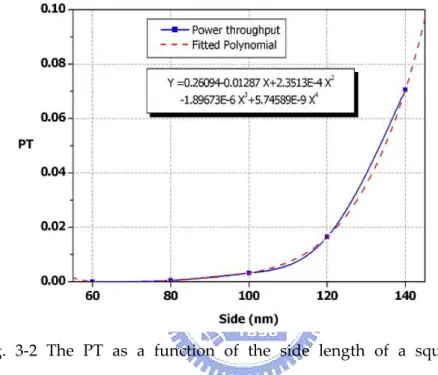
(nc) indices... ‐ 21 ‐ Fig. 2‐4 Geometric relationship between longitudinal and transverse components β, κ of the wavevector k... ‐ 22 ‐ Fig. 2‐5 (a) A buried waveguide and its equivalent structure: (b) a thin and (c) a thick waveguide ... ‐ 24 ‐ Fig. 2‐6 |E|2 distribution at 48 nm from (a) C‐shaped, (b) square, and (c) modified C‐shaped apertures and |E|2 cross section along (d) X and (e) Y axis... ‐ 25 ‐ Fig. 2‐7 Schematic illustration of surface plasmons propagating along the dielectric‐metal interface induced by a p‐polarized incident light .... ‐ 27 ‐ Fig. 2‐8 Dispersion curve of surface plasmons and incident light... ‐ 28 ‐ Fig. 2‐9 Excite surface plasmon polaritons by (a) a grating structure and (b) attenuated total reflection... ‐ 29 ‐ Fig. 2‐10 Transmission spectrum of (a) a circular aperture surrounded with a corrugation structure and (b) a hole array ... ‐ 30 ‐ Fig. 2‐11 Configuration of a hole array in a metal film sandwiched with two dielectric materials... ‐ 31 ‐ Fig. 3‐1 Dimensional parameters of (a) a C‐shaped aperture and (b) a groove surrounding a C‐shaped aperture and transmission model through (c) a C‐shaped aperture, (d) a C‐shaped aperture surrounded with a corrugation, and (e) a C‐shaped aperture with oblique illumination ‐ 39 ‐ Fig. 3‐2 The PT as a function of the side length of a square aperture ... ‐ 42 ‐ Fig. 3‐3 The PT as a function of gap g with various ridge lengths c ... ‐ 43 ‐
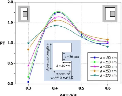
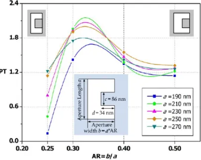
Fig. 3‐4 The PT as a function of aspect ratio AR with various aperture lengths a as ridge width d is 46 nm ... ‐ 44 ‐ Fig. 3‐5 The PT as a function of aspect ratio AR with various aperture lengths a as ridge width d is 34 nm ... ‐ 45 ‐ Fig. 3‐6 The PT as a function of the interval i with various widths w... ‐ 47 ‐ Fig. 3‐7 The PT as a function of pitch p with various interval i ... ‐ 48 ‐ Fig. 3‐8 The PT as a function of the interval i on the exit plane with various widths w... ‐ 50 ‐ Fig. 3‐9 The power throughput (PT) at a distance of 50 nm from the aperture and reflection coefficient rp as a function of the incident angle ... ‐ 52 ‐ Fig. 3‐10 (a) Ez, (b) Ex, and (c) Hy field profile, and (d) magnitude of Poynting vector plot when the incident angle is 44 degree. The dashed line showed the contour of the metal film and the C‐aperture... ‐ 54 ‐ Fig. 3‐11 The spectral response of the power throughput through the C‐shaped aperture with a incident angle of 44 degree ... ‐ 55 ‐ Fig. 3‐12 Electric intensity distribution inside the waveguide at a position of (a) 1/4, (b) 1/2, (c) 3/4 of the length from the entrance plane when propagating along the waveguide, and (d) the power throughput decay as a function of the distance from the waveguide ... ‐ 56 ‐ Fig. 3‐13 Power throughput as the waveguide scales up or down by the scale factor in the model of 44‐degree illumination... ‐ 57 ‐ Fig. 4‐1 Fabrication process of a free‐standing metal film (a) deposit silicon nitride on silicon wafer, (b) pattern on photo resist, (c) remove silicon nitride by RIE, (d) wet etch using KOH, (e) deposit silver film, and (f) remove silicon nitride by ICP‐RIE ... ‐ 60 ‐ Fig. 4‐2 Parameters determining the quality of a special‐shaped aperture ... ‐ 62 ‐ Fig. 4‐3 Operation modes of an apertured NSOM (a) illumination, (b) collection, (c) illumination collection, (d) reflection, and (e) reflection collection ... ‐ 65 ‐ Fig. 4‐4 Configuration of far‐field measurement system... ‐ 68 ‐ Fig. 4‐5 SEM photos of (a) a circular aperture, (b) a C‐shaped aperture, and (c) a C‐shaped aperture surrounded by a groove ... ‐ 70 ‐ Fig. 4‐6 SEM photo of a single C‐shaped aperture for oblique illumination.... ‐ 70 ‐ Fig. 4‐7 Intensity distributions measured by NSOM (a) background noise and (b) the C‐shaped aperture ... ‐ 74 ‐ Fig. 4‐8 Near‐field distribution observed by NSOM with (a) normal and (b) 44‐degree incidence... ‐ 74 ‐ Fig. 4‐9 Calculated electric intensity distribution at 50nm from the
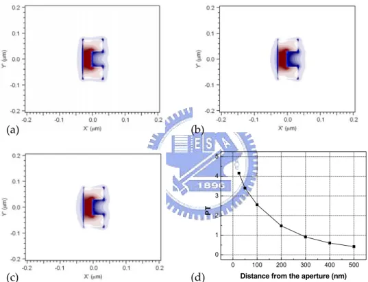
nano‐waveguide with the experimental dimensions at (a) normal incidence and (b) 44‐degree incidence... ‐ 75 ‐ Fig. 4‐10 Calculated (a) Ex and (b) Ez field profile with the experimental dimensions ... ‐ 75 ‐ Fig. 5‐1 Schematic illustration of system configuration ... ‐ 78 ‐ Fig. 5‐2(a) Configuration of an external‐cavity laser diode with a length of fiber and (b) an equivalent laser diode ... ‐ 80 ‐ Fig. 5‐3 Simulated self‐mixing interferometric fringe ... ‐ 81 ‐ Fig. 5‐4 (a) Experimental setup for feedback signal characterization and (b) measured signal from the photodiode... ‐ 82 ‐ Fig. 5‐5 Comparison of a measured feedback signal and a calculated self‐mixing interferometric signal ... ‐ 83 ‐ Fig. 5‐6 (a) photo of the pickup with laser diode mounted and (b) side view of modified laser package ... ‐ 84 ‐ Fig. 5‐7 (a) Angular variation of the disk and the laser size determines the approach limit and (b) the measured angular variation of the glass disk at different radial position along tangential and radial direction ... ‐ 85 ‐ Fig. 5‐8 (a) Measured open‐loop frequency response of the actuator and (b) calculated step response of the actuator according to the modeling transfer function... ‐ 86 ‐ Fig. 5‐9 Block diagram of the gap sensing probe system ... ‐ 87 ‐ Fig. 5‐10 Open‐loop frequency response of the active height control system . ‐ 88 ‐ Fig. 5‐11 (a) Configuration of actuated surface test system and (b) experimental results when the displacement of the actuated surface is 4.8 μm at 1500 rpm... ‐ 90 ‐ Fig. 5‐12 (a) Configuration of spinning disk test system and (b) experimental results with a disk runout of 16 μm at 1500 rpm ... ‐ 91 ‐
Chapter 1 Introduction
1.1 Introduction to Data Storage System
Based on the recording mechanism, data storage can be classified into three groups: electric, magnetic, and optical storage systems. In electric storage systems, information is stored in the form of electric charges, either in transistors or capacitors. Magnetic storage systems store information in the magnetic state of atoms of recording medium, which is written by an external magnetic field and read out by a magnetic transducer. Instead, optical storage systems store information by the modulation in the reflectivity of disk surfaces, for example, by either physical structures or crystalline states [1].
In contrast to electric storage, magnetic and optical storage systems have features in common. Both of them require a pickup head to fly over disk surfaces for recording or picking up data on the disk so that a flying head and a servo control system are essential components in these two types of systems. Furthermore, the capacity of these two systems is comparatively higher than that of electric storage systems. However, data access rate of magnetic and optical storage systems is relatively low compared to that of electric ones. Therefore, both magnetic and optical storage systems are categorized in the secondary memory for storing and backing up data while electric storage systems are used as the primary memory for processing information. Because of divergences in the nature between the primary and the secondary memory, our study will focus only on the secondary memory.
Due to the explosively increasing demand for storing information as multimedia is spread out over the world and widely used in daily life, data storage systems with higher recording capacity are undoubtedly desired.
Moreover, mobility, miniaturization and power consumption are also considerable issues in data storage systems. Therefore, those requirements drive the development of storage systems toward higher recording density and efficiency. A road map of optical storage systems shown in Fig. 1‐1 illustrates an example of the development of the storage capacity. From the first CD launched in the 80s to the latest near‐field disc, the capacity increases hundreds times or even higher. However, the increase of the recording density is not unlimited. The principles of recording mechanisms and the physical characteristics of recording materials determine the theoretic ceiling of the recording density.
Fig. 1‐1 Road map of optical storage systems
In magnetic storage systems, the recording density depends on mark sizes, i.e. a minimum magnetic domain. With the decrease of mark sizes, grain sizes in the recording medium must be smaller than the mark sizes to obtain a sufficient signal‐to‐noise ratio. However, if grain sizes are too small, random thermal fluctuations cause magnetic domain switching and consequent destruction of data in a conventional recording medium. The size at which the magnetic state of a grain is no longer thermally stable is the so‐called super‐paramagnetic limit. The criterion for thermal stability is shown in Eq. (1‐1) as below [2], 0.1 1 10 100 1000 1975 1985 1995 2005 2015 2025 Year of Introduction Ca pa ci ty ( G B) ~15% / year DVD 4.7 GB 650 nm 0.6 NA CD 0.7 GB 780 nm 0.45 NA Near Field ~150 GB 405 nm 1.5-2.0 NA BD/HDVD 25 GB 405 nm 0.85 NA
70 > T k V K B u , (1‐1)
where Ku is the uniaxial anisotropy coefficient, V is the grain volume, kB is
Boltzmann’s constant, and T is temperature. Although some recording materials have a sufficiently large Ku for thermal stability, the coercivity of these materials
at room temperature is too large to be switched by an external magnetic field generated by conventional heads. One solution to overcome this issue is to introduce a heat‐assistance method by employing a laser beam to heat a local area of the recording material. When the temperature of the medium is close to its Curie point, the coercivity drops dramatically so that only a small magnetic field is needed to record data in the medium. Therefore, an optical system that can confine sufficient optical power into a spot with a diameter of less than 50 nm is necessary for heat‐assisted magnetic recording (HAMR) [3]. In optical storage systems, a laser stylus, a spot focused by an objective lens, is used to illuminate disk surfaces. The reflected light from the disk surface is collected by the objective lens and delivered to an optical detector. The storage density is dependent on the spatial resolution of the laser stylus, which corresponds to the spot size of the optical system. According to the diffraction theory, the theoretic minimum spot size of a far‐field focusing system, also called the diffraction limit, is proportional to the ratio of the incident wavelength to the numerical aperture (NA) of the optical system,
NA
d∝ λ , (1‐2)
where d is the diameter of the focused spot, λ is the incident wavelength, and
NA is the numerical aperture. Thus, the only way to increase the storage density
is to reduce the wavelength or increase the numerical aperture. However, aberrations, which are inversely proportion to the square or cubic of the spot size, become significantly worse with the decrease of the wavelength or the increase of NA.
Therefore, in order to break through the theoretic limit, both magnetic and optical storage systems need an optical system that can bring a subwavelength spot to the recording medium. According to near‐field theories, in a distance of less than a wavelength from optical devices, evanescent waves are taken into account and thus the field behavior is distinctively different from that after propagating far away from the devices. Because the evanescent waves have higher spatial frequency information than that of the propagating waves, a subwavelength spatial resolution beyond the diffraction limit can be obtained in the near field. Since the evanescent waves decay exponentially with the distance from the optical device, the spacing between the device and the medium surface has to be kept within a wavelength, typically less than 100 nm. Therefore, remaining the spacing with nanoscale precision is a challenging issue for near‐field optical systems.
1.2 Near-field Optical System
A near‐field optical system uses near‐field optical techniques to achieve subwavelength resolution. However, challenging issues accompany the shrinkage of spot sizes and gaps between optical devices and media. Based on mechanisms employed, near‐field optical systems are categorized in two groups, subwavelength apertures and solid immersion lenses, and explained in the following.
1.2.1 Subwavelengh Aperture
1. PrincipleA subwavelength aperture in a metal films blocks part of incident fields to confine optical energy into a tiny area, as shown in Fig. 1‐2. Subwavelength resolution of λ/20 was first demonstrated by employing a nano‐aperture in
Incident Light Subwavelength spot Nano-aperture Metal Film near‐field microscopy [3]. This novel breakthrough gave the birth to near‐field scanning optical microscopes (NSOM) and opened a new avenue of near‐field optics [4‐8]. In conventional NSOMs, a tapered fiber probe was used to generate a tiny stylus for resolving the image. By depositing a metal film on the side wall of the stylus, a nano‐aperture with a symmetric shape was consequently formed at the tip. Fig. 1‐2 Schematic illustration of a subwavelengh aperture
Subwavelength apertures have advantages of simple configuration and easy fabrication. However, because the field inside the fiber suffered a serious energy loss in the tapered area and through the aperture, the transmission of a tapered fiber probe typically ranged from 10‐3 to 10‐5 [9‐11]. Thus the picked‐up
signal was relatively noisy and complex signal processing was necessarily required in the system. Therefore, a lot of effort was made to increase the transmission of subwavelength apertures.
(1) Special‐shaped Apertures
Special‐shaped apertures were designed to enhance the transmission by exciting either radiation from the aperture which functions as an antenna or propagation modes inside the aperture. A bow‐tie antenna or dipole antenna was proposed to generate radiation from resonance of electric fields on the
antenna induced by incident waves, as shown in Figs. 1‐3 (a) and (b) [12‐14]. The resonance coupled from incident light, highly dependent on the geometry and dimensions of the antenna, radiated electromagnetic waves and thus generated a spot of a diameter much less than a wavelength. An alternative approach was to employ an aperture as a waveguide. Either a C‐ or I‐shaped aperture functioning as a ridge waveguide supported propagation modes and thus reduced the energy dissipation through the aperture [15‐19]. According to waveguide theories, the propagation modes of a waveguide are particular patterns of field which fulfill the boundary condition and can propagate through the waveguide without significant energy loss. The refractive indices and the geometry of the waveguide determine the propagation modes that can be supported inside the waveguide. Therefore, the dimensions of the aperture dominate the transmission and the spot size through the aperture. Fig. 1‐3 (a) A bow‐tie antenna and (b) dipole antennas (2) Surface Plasmon Polaritons
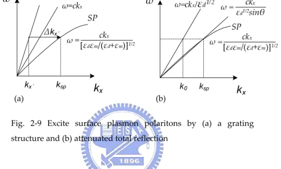
Another solution is to induce the surface plasmon excitation in dielectric‐metal interfaces of a metal film [20‐23]. The resonance of surface plasmon polaritons induced by the incident light will result in oscillation of
electrical fields and re‐radiation in the vicinity of the film surface. The metal structure itself then functions like an active light source. It means that the resonance of surface plasmons modes on both sides of a metallic film makes the energy transfer between incident light and surface plasmons as well as between surface plasmons and emitted light possible. Consequently, under a proper design, the energy carried by photons obstructed behind the film contributes to the transmission through the film and thus breaks through the theoretic limit. Unfortunately, because the dispersion curve of surface plasmons lies right of the light line of the same energy, surface plasmons have a longer wave vector than that of light. An additional wave vector has to be added to excite surface plasmons by introducing periodic structures, such as hole arrays and corrugations, or attenuated total reflection.
2. Gap Control
For a conventional NSOM fiber probe, the shear force method is used to detect the spacing between the probe tip and sample surfaces, as shown in Fig. 1‐4 [24]. The fiber probe is attached on a tuning fork which is driven by a piezo actuator. In the absence of the sample surface, the fiber probe with the tuning fork is driven to resonate at its nature resonant frequency. As the fiber probe is approaching to the surface, the shear force between the fiber tip and the sample surface alters the resonant amplitude and then can be detected by the piezo actuator which can alternatively function as a sensor.
Because the change in the resonant amplitude is a function of the gap and then can be used as a feedback servo signal, the shear force method has an advantage of extremely high sensitivity. Typically, a residual position error of less than 0.1 nm can be achieved. However, since the amplitude of the feedback signal is too low to be detected, the signal‐to‐noise ratio (SNR) is so low that a complicated signal processing system is required to filter out the signal.
Fig. 1‐4 Configuration of a conventional NSOM fiber probe and a sample surface
1.2.2 Solid Immersion Lens
1. Principle Fig. 1‐5 Schematic illustration of a solid immersion lensSince the diffraction limit is determined by the ratio of the incident wavelength to the numerical aperture, the spot size of far‐field optical systems can be further reduced by increasing the effective NA if the incident light experiences a refractive index of greater than air. As a result, a semi‐spherical solid immersion lens (SIL) was proposed to insert into the optical path of a focusing beam, as shown in Fig. 1‐5 [25‐27]. The incident light which arrived at the bottom of the solid immersion lens at an angle of greater than the critical angle suffered a total internal reflection at the dielectric‐air interface where evanescent waves were generated and penetrated through. Spatial resolution
Disk θc Propagating wave Ev anescent wav e Air gap Δz SIL Objective
can be improved by a factor of refractive index of the material of SIL because evanescent waves carried information with higher spatial frequencies. However, the amplitude of evanescent waves dropped exponentially with an increase of the distance from SIL. An extremely precise gap control system was necessary for remaining the spacing between the SIL and the medium less than a wavelength, typically less than 100 nm in the case of blue lasers [28‐29]. Moreover, a semi‐spherical SIL was difficult to fabricate and also too bulky to be integrated into flying heads.
2. Gap Control
In a solid immersion lens system, when a surface is in close proximity to the bottom of the solid immersion lens, the coupling between the evanescent wave and the surface will generate an orthogonal polarization component to the reflected field. And the polarization component decays as the increase of the spacing between the surface and the bottom of the SIL. Therefore, a polarized beam splitter is used to filter out the orthogonal component and then the filtered reflected power is a function of the spacing, as shown in Fig. 1‐6 [30]. The linear region of this signal can be used as a feedback signal to remain the spacing with nanoscale precision.
Similar to the shear force method, the reflected power method also has an advantage of high sensitivity. A residual position error of less than 5 nm was successfully demonstrated. However, a complex optical system is necessary for delivering and filtering optical signals. Due to numerous lenses, the alignment among those lenses becomes a challenging issue.
1.3 Dual-probe fiber head
Upon the demand of recording density, either magnetic or optical storage systems require a near‐field light source with active gap control that can confine optical power into a subwavelength spot with sufficient transmission. A conventional fiber probe has advantages of compactness, ease of fabrication, and integration capability; however, low transmission results in high power consumption and heat dispersal issues. The gap control employing shear force between the fiber tip and the sample surface as the feedback signal encounters an issue of low speed and low SNR. In contrast, solid immersion lens efficiently brings optical power to the medium but a complex and costly process is necessary for fabricating the SIL. In addition, the SIL is too bulky to be installed on a flying head and significantly degrades the dynamic characteristics of the optical head. The reflected power method used for focusing servo control requires a complicated external optical system to filter out and process the signal.
Due to the issues that conventional systems encounter, by taking advantage of fiber for compactness, lightness, simplicity, and integration capability, we propose a novel dual‐probe near‐field fiber head system. The system consists of a straw‐shaped writing probe that delivers optical power to the medium and a gap sensing probe that detects the spacing and sends a feedback signal to the controller. The writing probe with a straw shape yields a high transmission
resulting from the hybrid effect we discover and the gap sensing probe exhibits nano‐scale precision as a result of the self‐mixing effect.
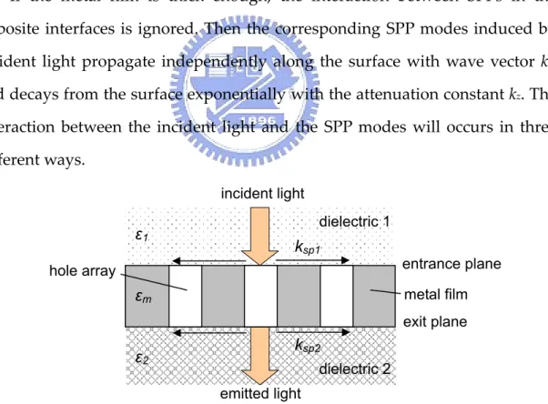
The system configuration is schematically illustrated in Fig. 1‐7. In the writing probe, a 1X2 10/90 fiber coupler is inserted into the optical path to split the light into two. 90% of the light goes to the straw‐shaped probe, where the end face is coated with a metallic film and perforated by a C‐shaped aperture at the center, while the remaining 10% light goes to the bare flat reference probe where the emitted power is measured to monitor the output from the straw‐shaped probe. In the gap sensing probe, the spacing between the probe end and the target surface functions as an external cavity for the laser diode. The interference between the reflected light and the field inside the laser cavity modulates the output power as a function of the spacing. The output power is detected by the photodiode and sent to the controller as a feedback signal. The dual‐probe fiber head is installed on a conventional biaxial actuator driven by the controller to maintain the spacing with nanometer position precision. Fig. 1‐7 Schematic illustration of the configuration of a dual‐probe fiber head system
1.4 Objective
The objective of this thesis is to present an efficient, miniaturized, compact, highly integrated dual‐probe fiber‐based optical head with simple and precise gap servo control. The dual‐port fiber head consists of a straw‐shaped writing probe with a subwavelength C‐shaped aperture and a gap sensing probe employing a self‐mixing laser sensor. To resolve the issue of low transmission through a subwavelength aperture in conventional fiber probes, we propose a novel configuration, a C‐shaped aperture surrounded by corrugations or illuminated with obliquely incident light, to excite a hybrid effect. Propagation modes and surface plasmon waves exist simultaneously and contribute to the
further enhancement of transmission through the waveguide. A
high‐transmission writing probe is then designed and realized by employing the hybrid effect. On the other hand, to overcome the issue of a complicated optical system that conventional detecting methods need, we design a gap sensing probe employing self‐mixing interferometric effect. We characterize the modulation of output power as a function of the spacing between the probe and the disk surface and use it as a feedback signal. According to the feedback signal, we also design a controller and circuits for driving a conventional biaxial actuator to remain the spacing with nanometer position precision.
1.5 Organization
In Chapter 2, we review theories of near‐field transmission, including Bethe’s theory, waveguides, and surface plasmons. Based on those theories, in Chapter 3, we propose a novel optical design, a C‐shaped aperture in a metal film as a waveguide surrounded with a circular corrugation or illuminated with obliquely incident light. This design induces a hybrid effect consisting of propagation modes inside the waveguide and surface plasmon modes in the
dielectric‐metal interfaces to enhance the transmission through the aperture. Modeling and optimization of this design are presented. The simulation results, including mechanisms of the hybrid effect and the transmission enhancement, are also explained and discussed. In Chapter 4, the fabrication of hybrid‐effect apertures and measurement instruments are presented and followed by the experimental results that demonstrated the proposed hybrid effect.
Chapter 5 focuses on the development of a near‐field servo control system employing a self‐mixing interferometric laser sensor. We characterize the interferometric signal in a laser diode and realize a laser sensor by modifying a commercial laser diode. The frequency response of a biaxial actuator with a laser sensor installed is measured and a controller is designed for the laser sensor system accordingly. Under an actuated surface test system and a spinning disk system, we demonstrate the operation of a near‐field control system using a laser sensor on a biaxial actuator.
The summary of the findings and throughputs of this thesis is presented in Chapter 6. We also suggest prospective works for near‐field light delivery systems.
Chapter 2 Theories of Near-field
Transmission
In this chapter, we briefly review the relevant literature on near‐field transmission through subwavelength apertures. Based on the assumption of a perfect conducting film, Bethe revealed that the transmission through a subwavelength aperture is proportional to the fourth power of the aperture size. Although some premises of Bathe’s theory do not work out well in the real world, it still discloses a theoretic fundament of the transmission through a subwavelength aperture. A lot of effort thus has been made to break through the theoretic limit. Special‐shaped apertures that can function as waveguides are one of promising solutions. If an incident field couples into propagation modes supported by a waveguide, the field can propagate through the waveguide with less energy dissipation. On the other hand, the oscillation of surface plasmon waves on both sides of a metallic film results in the enhancement of the transmission if the satisfaction of the momentum matching condition induces coupling between incident photons and surface plasmon polaritons. Propagation modes of a waveguide and surface plasmon polaritons stimulate the development of a hybrid effect, which is the fundamental theory of a novel light source system we propose.
2.1 Bethe’s Theory
Consider a normal incident light impinging on a perfect conducting film at plane z=0, which divides the space into two parts: the left space of z<0 and the right one of z>0, as shown in Fig. 2‐1 [31]. Assume E0 and H0 to be the field onthe lefthand side of the film if there is no aperture. The field fulfills the boundary conditions for z=0,
0 0 r r r× E = n (2‐1a) 0 0 = ⋅ H nr r (2‐1b)
Fig. 2‐1 Model of Bethe’s theory
The field on the right hand side vanishes identically and the zero approximation field satisfies the boundary condition everywhere on the film but not in the aperture where H and the normal component of E are discontinuous. The field is written as 1 0 H H Hr = r + r for z<0 (2‐2a) 2 H Hr = r for z>0 (2‐2b) Then the boundary conditions are: tan 2 tan 1 E Er = r in the aperture (2‐3a) tan 0 tan 1 tan 2 H H Hr − r = r in the aperture (2‐3b) 0 tan 2 tan 1 = E = Er r for z=0 outside the aperture (2‐3c)
If we assume the aperture is symmetric with respect to z=0, x and y components of E as well as zcomponent of H automatically fulfill the condition of symmetric distribution. Then Eqs. (2‐3a) and (2‐3b) are rewritten in the
following form: z z E E2 0, 2 1 r r = (2‐4a) tan 0 tan 2 2 1 H Hr = r (2‐4b)
Since the aperture size is extremely small compared to the wavelength λ,
H0x, H0y, and E0z are approximated as constants over the aperture. Moreover, the aperture shape is assumed to be circular with radius a. By introducing Stratton’s formula, E is represented by a full‐vector theory [33]. ] ) ( )) ( ( ) ( [ 4 1 ) ( σ φ φ φ π × − × ×∇ − ⋅ ∇ =
∫
d ikn H r n E r n E r r Er r r r r r r (2‐5)In the absence of electric charges or electric currents, the first item in the integral equation can be omitted. Consequently, magnetic current density K and surface charge density η are introduced as the sources of the electric field in the aperture. The continuity equation corresponding to magnetic current density and surface charge density is fulfilled. The time dependence of all quantities is assumed to be harmonic oscillation. eiωt and ω=cκ (2‐6) The electric field E and magnetic field H can be expressed in terms of K and η with the aid of scalar potential Ψ and vector potential F: F Er=∇× r (2‐7a) Ψ ∇ − ∂ ∂ = t F c H r r 1 (2‐7b) where F and Ψ are in exact analogy to the electric case, which is represented by the integral of K and η over the plane of z=0, ' ) ' ( ) ' ( ) (r K r r r dr Fr =−
∫
φ − (2‐8a)' ) ' ( ) ' ( ) (r = r r−r dr Ψ
∫
η φ (2‐8b) In Eqs. (2‐8a) and (2‐8b), φ is the retarded radiation between the source vector r’ to the field vector r, as shown in Fig. 22. Fig. 2‐2 Diagram of source point and field point By inserting these results into Eqs. (2‐7a) and (2‐7b), E and H can be obtained by the integral of magnetic surface current K and charge η over the aperture area. σ d r K r Er( )=∫
r( ')×∇Φ (2‐9a)∫
Φ− ∇Φ = iκK r η r dσ r Hr( ) [ r( ') ( ') ] (2‐9b)Based on the assumption that the aperture size is much smaller than the wavelength, H is considered as a static field corresponding to the surface charge density η. Thus, the first term in Eq. (2‐9b) is neglected. Then we assume a constant magnetic field component Htan equal to ½H0 over the aperture. In
addition, the retardation term in Eq. (2‐8b) is also omitted because the field point is in proximity to the aperture. Under these assumptions, the scalar potential is written as r H r r dr r r =− r ⋅r − = Ψ
∫
0 2 1 ' ' ) ' ( ) ( η (2‐10)This constant field is produced by a uniform distribution of dipoles in an ellipsoid, of which the direction is identical to that of the field. If the axis of the ellipsoid is assumed to be small, the cross section of the ellipsoid in XY plane
should be equivalent to the aperture area. Thus, the surface density of dipoles μ is proportional to the ordinate of the ellipsoid: 2 1 2 2 ) ' (a −r = μ (2‐11) The surface charge density η is then in the form of 2 1 2 2 0 ) ' ( ' r a r H C − ⋅ − = r r η (2‐12) where C is a proportional constant. Then the magnetic surface charge density η and current density K are 2 1 2 2 2 0 ) ' ( ' r a r H − ⋅ − = π η r r (2‐13a) 2 0 2 1 2 2 ) ' ( π H r a ik K r r = − (2‐13b)
From Eq. (2‐9a), it is clear that the distribution of the surface magnetic current density K obtained in Eq. (2‐13b) does not contribute appreciably to E. In Eq. (2‐13b), the K is of the order of kaH0 and grad Φ is of order 1/a2. The
integral in Eq. (2‐9a) over an area of order a2 makes the contribution of current
density K to E of order kaH0. Therefore, the normal component of E0 shall be of
the same order as H0. An additional magnetic current distribution KE then is
necessary for matching the boundary condition for En. This new current
distribution, however, does not give rise to any extra magnetic charge density η. Thus, KE must be: 0 = ⋅ ∇ KrE (2‐14) According to Eq. (2‐7a) we can obtain r E Fr = r0×r 4 1 (2‐15)
and from Eqs. (2‐10) and (2‐13a), the current for the required E is 2 1 2 2 2 0 ) ' ( 2 ' r a E r KE − × = π r r r (2‐16) Then the total magnetic current density in the aperture is ] ) ' ( 2 ' ) ' ( [ 1 2 1 2 2 0 0 2 1 2 2 2 r a E r H r a ik K K K H E − × + − = + = r r r r r π (2‐17) while the magnetic charge density is the same as Eq. (2‐13b).
According to Eqs. (2‐9a), (2‐9b), and (2‐17), E and H can be obtained by imposing them into Maxwell equations: ) ˆ 2 ( ˆ 3 1 0 0 0 3 2 r E H r a Er = κ φ × r + r × π (2‐18a) ) ˆ 2 ( ˆ 3 1 0 0 0 3 2 E r H r a Hr =− κ φ × r × − r π (2‐18b)
where Φ0 = eikr / r for r’=0 and rˆ is unit vector in the direction of rr. Then, the
Poynting vector S of the diffracted field is: 2 0 0 2 6 4 2 (2ˆ ˆ ˆ ) ˆ 36 1 4 r r H r r E r a H E c Sr= r× r = κ × r − × × r π π (2‐19) and the total transmitted radiation in all directions is: ) 4 ( 27 sin 2 2 6 02 0 2 2 0 2 2 / 0 E H a c S r d d Stotal =
∫
⋅∫
r = κ r + r π α θ θ π π (2‐20)The solution indicates that the total transmitted radiation through an aperture is proportional to the sixth power of the aperture size a. If we define the power throughput (PT) as the ratio of the total transmitted power to the incident power over the aperture. According to Bethe’s theory, PT of a subwavelength aperture is proportional to the fourth power of the aperture size. Although this analytical solution provides a fundamental theory for calculating the transmission through an aperture, there are some theoretic restrictions and
premises. First, the metallic screen is assumed as a perfect conductor. Second, the assumption of symmetry of the aperture simplifies the field distribution. Furthermore, this solution is valid only when the aperture size is much smaller than the wavelength. Even through some literatures tried to modify Bethe’s formula for greater accuracy, it is still impossible to derive analytical solution without any approximations and assumptions, especially for complex‐shaped apertures. Therefore, in this thesis, we employ Finite‐Difference Time Domain method (FDTD) to calculate power throughput and field profiles through our designed apertures.
2.2 Waveguide Theory
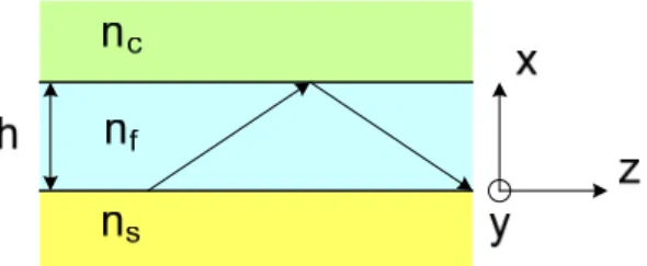
A waveguide is a special‐designed structure that can guide waves through a long distance with acceptable energy loss. A typical waveguide structure consists of a high‐index dielectric layer with a height h sandwiched with two lower‐index materials, as shown in Fig. 2‐3 [32]. The index of refraction of the guiding slab nf must be larger than that of the cover material nc or the substrate
material ns in order for total internal reflection to occur at the interfaces. If the
slab is ideally infinite in extent in the yz plane, but finite in x direction, we can develop a basic form of guided modes using boundary conditions, which is applicable to real problems.
Fig. 2‐3 A typical planar waveguide consisting of three layers arranged that guiding index of refraction (nf) is larger than the
For a sinusoidal transverse electric (TE) wave with a wave vector k and frequency ω0, the wave equation in each region can be put in the scalar form: 0 2 2 0 2 + = ∇ Ey k niEy (2‐21)
where ni = nf, ns, or nc. Because the slab is infinite in y direction, Ey is a function
of both x and z but independent of y. Due to the translational invariance of the structure along z direction, we assume that the amplitude does not vary along z axis but the phase does. If we choose a trial solution to Eq. (2‐21) in the form: z j y y i e x E y x E ( , )= ( ) − β⋅ (2‐22) where β is a propagation coefficient along z direction. Then by putting Eq. (2‐22) into Eq. (2‐21), we can obtain 0 ) ( 2 2 2 0 2 2 = − + ∂ ∂ y i y E n k x E β (2‐23) In the case β > k0 ni, we have a general solution with a real exponential form: x n k y i e E x E 2 02 2 0 ) ( = ± β − (2‐24a) where E0 is the field amplitude at x = 0. This solution is the evanescent field of a total internal reflected wave at an interface. In the case β < k0 ni, the solution has an oscillatory form: x n k j y i e E x E 02 2 2 0 ) ( = ± −β (2‐24b)
Fig. 2‐4 Geometric relationship between longitudinal and transverse components β, κ of the wavevector k
x
z
k
κ
If a transverse wavevector κ is defined as 2 2 2 0 β
κ = k ni − , β and κ are
geometrically related to the total wavevector k = k0 ni, as shown in Fig. 2‐4,
inside the guiding layer.
The longitudinal wavevector β is used to identify individual modes and also defined as the eigenvalue of the mode. A guided wave must satisfy the condition, k0 ns < β < k0 nf (2‐25) where it is assumed that nc ≤ ns. To find the values of β that lead to solutions to the wave equation, the boundary condition is applied to Eqs. (2‐24a) and (2‐24b). Then the transverse electric field amplitudes in the three regions are x y c Ae x E ( )= −γ 0 < x (2‐26a) ) sin( ) cos( ) (x B x C x Ey = κf + κf ‐h < x < 0 (2‐26b) ) ( ) ( x h y c De x E = −γ + x < ‐h (2‐26c)
where A, B, C, and D are amplitude coefficients to be determined, γc and γs are
attenuation coefficients in the cover and substrate, respectively, and κf is the
transverse component of k in the guiding layer. According to the boundary condition that tangential component of field is continuous at the interfaces, the characteristic equation to get the eigenvalue of propagation coefficient for a TE wave is ) 1 ( ) tan( 2 f s c f s c f h κ γ γ κ γ γ κ − + = (2‐27) The characteristic equation clearly shows that the propagation mode supported by the waveguide is highly dependent on the refractive indices of materials and the dimension of the guiding layer, height h.
For a complex waveguide, a two‐dimensional structure can be decomposed into two spatially orthogonal waveguides: a horizontal and a vertical slab waveguide. The propagation coefficient β of the waveguide can be found by using the solutions to these two orthogonally oriented waveguides based on the techniques developed. This method is known as the effective index method. Consider a buried rectangular waveguide shown in Fig. 2‐5. The waveguide is decomposed into a thin waveguide and a thick one. The thin part is analyzed in terms of the actual indices of the structure; while the thick part is analyzed using the effective index from the first analysis. Fig. 2‐5 (a) A buried waveguide and its equivalent structure: (b) a thin and (c) a thick waveguide
Once the propagation coefficient β of the thin slab waveguide is obtained for a specific wavelength and mode of interest, the effective index of the slab is determined through the following expression 0 k neff β = (2‐28)
where k0 is the vacuum wavevector of the light being guided. The effective
index then is used to replace the original refraction index for the guiding layer in the thick waveguide to calculate the propagation coefficient of this waveguide. Then the value of propagation coefficient found from the last step is the value for the mode we want.