國立交通大學
材料科學與工程學系
博士論文
超低介電孔洞材料 MSQ 薄膜中起孔洞劑
聚集行為及孔洞形貌控制之研究
The porogen aggregation behavior, pore size,
and size control of ultra-low-k porous
organosilicate films based on MSQ/porogen
hybrid system
研 究 生:諶昱涵
指導教授:呂志鵬 博 士
超低介電孔洞材料 MSQ 薄膜中起孔洞劑聚集行為
及孔洞形貌控制之研究
The porogen aggregation behavior, pore size, and size control of
ultra-low-k porous organosilicate films based on MSQ/porogen hybrid
system
研 究 生:諶昱涵 Student:Yu-Han Chen
指導教授:呂志鵬 教授 Advisor:Dr. Jihperng Leu
國立交通大學
材料科學與工程學系
博士論文
A Thesis
Submitted to Department of Materials Science and Engineering
College of Engineering
National Chiao Tung University
in Partial Fulfillment of the Requirements
for the Degree of
Doctor of Philosophy
In Materials Science and Engineering
June 2012
Hsinchu, Taiwan, Republic of China
超低介電孔洞材料 MSQ 薄膜中起孔洞劑聚集行為
及孔洞形貌控制之研究
研究生:諶昱涵 指導教授:呂志鵬 博士
國立交通大學
材料科學與工程學系
摘 要
本研究使用延後移除高溫起孔洞劑製程(post-integration porogen removal scheme)的混合型低介電材料,主要分為三個部份:(1)探討起孔洞劑(poorgen)於低 介電母材中團聚的行為;(2)分散 porogen 於低介電母材中,並有效控制 porogen 以 及最後孔洞的尺寸;(3)提高母材中 porogen 的含量,致使更有效降低介電常數維持 更小孔洞,並探討其結構與性質間之關係。首先,選用methylsilsesquioxane (MSQ) 為母材,polystyrene-b-polybutadiene-b-polystyrene (SBS)作為高溫起孔洞劑,使之 形成混合型低介電材料薄膜。在不同升溫速率條件下利用即時動態的 grazing incidence small angle X-ray scattering (GISAXS)量測 porogen 尺寸變化;並以黏度變 化和紅外線光譜儀(FT-IR)分析母材結構對 porogen 尺寸的影響。藉由其交互行為可
得知 SBS 的團聚主要受三個關鍵的溫度影響; (1)母材的玻璃轉換溫度,此時開始 有團聚現象,(2)母材開始大量產生交鏈的溫度(或結構由 cage 轉換成 network 時), 此時團聚現象更甚,(3) 母材完成交鏈的溫度,此時結構固化,團聚不易產生。確 定團聚機制後,第二部分使用 polystyrene(PS)作為 porogen,並使用陰離子型的 dodecylbenzenesulfonate (NaDBS)以及陽離子型的 domiphen bromide (DB)界面活性 劑將porogen 進行表面改質,然後檢測慢速升溫(2oC/min)過程中的 porogen 尺寸及 黏度的變化。研究結果指出,改質過的porogen 表面帶有電荷,並存在庫倫力將其 排斥並穩定分散於母材中,而且在改質過後的porogen 造成的電滯效應使母材整體 黏度上昇,使之更不容易擴散或聚集於母材內。另一方面帶有正電的PS 會與 MSQ 母材中的Si−OH 有吸引作用,位置會被母材固定住致使更不易團聚,故可達到更 佳控制孔洞大小的效果。最後研究將DB 改質的 PS 增量於低介電母材中,用以增 加孔隙率並降低介電常數,結果指出孔隙率達到45vol.%以上,介電常數可有效降 低,且孔洞呈現獨立圓形,其機械性質因無內連結大型孔洞可維持強度。以往文 獻指出porogen 的含量大於 25wt%或孔隙率達到 30vol.%以上時,因為 porogen 大 量聚集而造成熱移除後的大型孔洞,本研究發展一個表面改質方法使porogen 可以 有效分散porogen 於母材中並能提高最後之孔隙率。
The porogen aggregation behavior, pore size, and size control of
ultra-low-k porous organosilicate films based on MSQ/porogen hybrid
system
Student: Yu-Han (Hans) Chen Advisor: Dr. Jihperng (Jim) Leu
Department of Materials Science and Engineering National Chiao Tung University
ABSTRACT
This work focuses on the hybrid low-k film in a late-porogen removal scheme. There are three parts are discussed including: (1) the aggregation behavior of porogen in the hybrid film; (2) disperses the porogen in the low-k precursor and control the porogne size (later pore size); (3) increases the loading of porogen in the low-k materials to reduce k value and try to remain the small pore size. Firstly, the interaction between polystyrene-b-polybutadiene-b-polystyrene (SBS) porogen and low-k methylsilsesquioxane (MSQ) matrix under different curing profiles and their impact on porogen size were studied by grazing incidence small angle X-ray scattering (GISAXS), viscosity measurement, and Fourier transform infrared analysis. The aggregation of SBS
porogen was greatly influenced by the microstructure of MSQ matrix at three controlling temperatures; namely (1) glass transition temperature, Tg (~100oC), (2) onset
temperature (160oC) for transforming cage to network structure, and (3) immobilization temperature (170oC). Secondly, an anionic surfactant, sodium dodecylbenzenesulfonate (NaDBS) and a cationic surfactant, domiphen bromide (DB) were used to modify the surface potential of PS porogen in the low-k film. The NaDBS- and DB-modified porogens with higher surface potential impede their aggregation within the cross-linking MSQ matrix, resulting in a smaller porogen size, by electrostatic repulsion and increased viscosity due to the electroviscous effect. In addition, the columbic attraction between Si−OH groups of MSQ matrix and the positively charged, DB-modified PS, restrains the PS porogen, thus reduces its aggregation during the curing step, leading to small porogen size and tight distribution at 200oC and later a similar pore size after removal of porogen at 400oC. Finally, the different loading of polystyrene (PS) porogen with/without cationic surfactant, domiphen bromide (DB) modification in MSQ appeared for porous low-k films. The pore size, morphology, mechanical strength and k of porous low-k films with different porosity were investigated. The porosity could be increased above 45 vol.% by porogen surface modification, and reduced k from 2.6 to 1.9. The porous film appear the no interconnect pore and maintain the sphere shape. The past paper indicates that porogen occur obvious aggregation at porogen loading>25 wt% (or porosity >30 vol.%). In this work, we develop a method of porogen surface-modification to disperse the porogen in the low-k materials and increase the porogen loading (porosity) effectively.
Acknowledgements
如果能夠重來一次,我不知道會不會再選擇攻讀博士學位。人生最可惜的地 方就是沒有如果,這是一趟單程的旅行,誰都沒有重頭啟程的機會跟權利,但是 換句話說,這也是生命最可貴的地方,沿路美麗的風景只有一次,旅途上的過客 或朋友甚至是敵人,都是無可替代的,所以才更應該珍惜與感激。 首先感謝我的指導教授呂志鵬老師,感謝老師這些年來在課業上的教導及協 助,除了訓練學生邏輯以及專業之外,老師也提供了很多待人處事的道理及應對 的方法,我覺得我不是一個好的學生,但老師非常的有耐心,雖然我跟老師的互 動相對而言比較少,但是我心裡是很敬重老師的。然後感謝協助完成論文的同步 輻射中心的23A 光束線成員,包括鄭有舜、蘇秋琿、蘇群仁、廖桂芬等,這些年 來在實驗數據上的解析及幫助。還有工研院化材所楊偉達、謝青城在流變黏度儀 上的協助。 接著謝謝實驗室的博士班成員。感謝同梯的好友徐國原在實驗及人生上的提 點,就像燈塔一樣指引了方向,也在我很低落的時候,告訴我建立價值跟重拾熱 情。謝謝車牧龍,感謝總會在我犯了過錯的時候提醒我,是我無話不談的好朋友, 也是實驗及生活上幫助我最多的人。謝謝徐幸鈴,在基礎理論上的教學及討論, 常常有聽君一席話,勝讀十年書那種茅塞頓開的體會。謝謝王智這個好兄弟一起 度過很多大風大雨的日子,常常在籃球以及課外活動上提攜我,是我最喜歡的一個有情有義的好朋友。謝謝徐明義好鄰居,我們一起坐的位子不知道幾年了,感 謝總是不厭其煩地幫我解決一些雞毛蒜皮的小問題,例如修電腦。感謝凃弘恩帥 哥,雖然沉默寡言存在感很低,但是有需要他的時候,他就會拿掉石頭帽子站在 第一線。另外感謝劉柏村,帶給我們實驗室不同領域的課外活動與無數的歡樂。 特別感謝姚奕全在最後口試以及論文上的協助以及幫忙。也感謝我多年來的好友 董憲澤,在學業及生活上的協助,以及提供很多冷笑話。 接著謝謝碩士班以及專題生成員。感謝鄧鈞元、陳冠宇、湯季高一起經歷半 夜睡實驗室的日子。感謝專題生楊麒瀚、姜翔耀、陳思漢在實驗上的協助。感謝 何瑜俢在運動健身上的陪伴。另外感謝有邱詩雅、黃少農、莊如瑛、陳欣源、徐 婉婷、許書豪、陳奎岳、胡勝翔、蔡沁穎、邱維剛、田丞芳、黨希昀、廖麒雅、 黃耀輝、周宏宇、蔡豐仰、梁宗琦、洪唯齡等在生活上的互相照應及幫助。 感謝我的女友孫珮容,在學業最後很難熬的這半年,每一天最快樂的時候, 就是能夠在電話裡說話的時候,雖然相隔兩地,但滿滿的鼓勵及甜甜的思念,總 是可以圍繞在我的身邊。最後感謝我的父親諶茂崧先生以及母親陳素蘭女士,在 經濟上的無條件支持,讓我可以沒有後顧之憂的完成學業。金錢是可以量化,計 算以及償還的,但是您們的愛是我花一輩子都無法還清的。所有的榮耀獻給我的 家人。 人生不能重頭開始,但是沒關係,心境可以從零開始,這樣的每一天,都會 是新的旅程。
Contents
Page 摘 要………i ABSTRACT ……….iii Acknowledgements ... v Contents………...vii Table Captions ... x Figure Captions ... xi Chapter 1 Introduction ... 1 1.1 Background ... 1 1.2 Overview ... 5Chapter 2 Literature Review ... 8
2.1 Backend interconnect challenges ... 9
2.2 Classification of dense low-k materials ... 12
2.2.1 Fluorinated Silicate Glass ... 13
2.2.2 Carbon-doped Oxide (CDO) ... 13
2.2.3 SiLKTM ... 14
2.2.4 Silsesquioxane based materials ... 15
2.3 Porous low-k materials ... 16
2.3.1 Silica aerogel and xerogel low-k dielectrics ... 17
2.3.2 Pure Silica-Zeolite low-k film ... 18
2.3.3 Nano-Clustering Silica (NCS) ... 19
2.3.4 Templated-type (porogen) low-k dielectrics ... 19
2.4 Selection of porogens ... 20
2.4.1 Linear amphiblic block polymer ... 20
2.4.2 Dendrimers polymer ... 21
2.4.3 Star-shape polymers ... 22
2.4.4 Cage supramolecules ... 23
2.4.5 Well-dispersion porogen ... 24
2.5 Challenges in porous low-k ... 26
2.5.1 Pore size ... 27
2.5.2 Porogen dispersion ... 28
2.5.3 Porogen loading and high porosity ... 29
2.6 Post-integration porogen removal scheme ... 31
Chapter 3 Experimental ... 60
3.1 Materials candidates ... 60
3.1.1 MSQ/porogen hybrid materials ... 60
3.1.2 Porogen surface modification ... 61
3.2 Sample preparation ... 61
3.2.1 The in-situ porogen activity test ... 61
3.2.2 Porogen modification ... 63
3.2.3 Different porosity low-k film with and without modification ... 65
3.2.3.1 Porosity ... 66
3.2.3.2 Pore size and porogen size ... 66
3.2.3.3 Electrical characteristics ... 67
3.2.3.4 Chemical characteristics ... 68
3.2.3.5 Mechanical strength ... 68
Chapter 4 Effect of Curing on the Porogen Size in the Low-k MSQ/SBS Hybrid Films ... 73
4.1 In-situ porogen size test ... 73
4.2 In-situ visosity test ... 76
4.3 Structure variation and porogen aggregation ... 78
4.4 Mechanical strength ... 83
4.5 Summary ... 84
Chapter 5 Effect of Surfactants on the Porogen Size in the Low-k Methylsilsesquioxane/Polystyrene Hybrid Films ... 92
5.1 Porogen size in the precursor ... 93
5.2 In-situ porogen size test ... 94
5.3 Pore size, distribution and porosity ... 96
5.4 Structure variation vs. porogen behavior ... 96
5.6 Dispersion mechanism ... 103
5.7 Summary ... 107
Chapter 6 Well-dispersed Ultra-Low-k Porous Methylsilsesquioxane using a Cationic Surfactant-modified Polystyrene Porogen ... 117
6.1 Porogen size in the precursor ... 118
6.2 Porosity and pore size, shape ... 119
6.3 Dielectric constant and mechanical properties ... 124
6.4 Summary ... 127
Chapter 7 Conculsions ... 136
References ... 139
Table Captions
Table 2.1 Type of ILD materials ... 33
Table 2.2 Principle properties of SSQ based dielectric materials ... 34
Table 2.3 Commercially available SSQ-based low-k materials. ... 35
Table 2.4 The pore size (nm) from PCL porogen under different low-k process ... 36
Table 2.5 The property of reactive-porogen on SSQ-based low-k materials ... 37
Table 2.6 The impact of porosity change on SSQ-based low-k materials. ... 38
Table 5.1 The zeta potential and the corresponding particle size of PS porogen in the solution as a function of surface modification. ... 109
Figure Captions
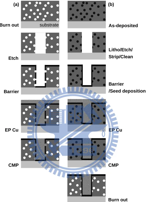
Figure 1.1 Formation schemes of porous low-k dielectrics in copper/low-k interconnects: (a) immediately after ILD deposition and (b) post-integration porogen
removal scheme after Cu CMP step forming a copper/low-k layer. ... 7
Figure 2.1 Industry average “Moore’s law” and chip size trends. ... 39
Figure 2.2 Device scaling projection trend shown in terms of gate length (half pitch) for Flash, DRAM, and MPU/ ASIC microelectronics products. ... 40
Figure 2.4 Decrease in interconnect delay and improved performance are achieved by using Cu and low-k dielectric. ... 42
Figure 2.5 Historical transition of ITRS low-k roadmap ... 43
Figure 2.6 Basic structure of FSG matrix. ... 44
Figure 2.7 Depiction of possible bond rearrangements upon SiOF film hydration to produce Si−OH bonding and the release of HF from the film. ... 45
Figure 2.8 Carbon-doped silica glass and schematic bonding structure ... 46
Figure 2.9 The typical precursors of CDO materials. ... 47
Figure 2.10 Organic SiLKTM chemical structure units. ... 48
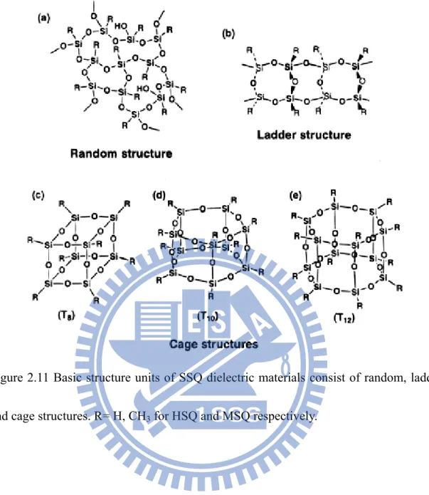
Figure 2.11 Basic structure units of SSQ dielectric materials consist of random, ladder and cage structures. R= H, CH3 for HSQ and MSQ respectively. ... 49
Figure 2.13 Schematics of the nano clustering silica (NSC) formulation and its film deposition and curing processes. ... 51
Figure 2.14 The conventional formation of porous low-k by using template-type porogen method. ... 52
Figure 2.15 Schematic structures of phase behaviors of PEO-b-PPO-b-PEO triblock .. 53
Fig. 2.17 Star-shape polymer porogens: PCL4, four-armed poly(ecaprolactone) and PCL6, six-armed poly(e-caprolactone). ... 55
Figure 2.18 β-Cyclodextrin (β-CD), a cage supramolecular porogen ... 56
Figure 2.19 The synthetic scheme: (a) sol-gel reaction and (b) ATRP method to prepare hybrid block copolymers based on MSQ. ... 57
Figure 2.20 The energy and the distance of relationship for two particles ... 58
Figure 2.21 The integration scheme of the post-integration porogen removal scheme. . 59
Figure 3.1 The molecular structure of (a) MSQ as the low-k matrix; (b) PS-b-PB-b-PS and (c) PS as the high-temperature porogens. ... 70
Figure 3.2 The molecular structure of surfactant: (a) NaDBs, and (b) DB. ... 71
Figure 3.3 Typical geometry of GISAXS measurement. ... 72 Figure 4.1 2-D GISAXS scattering patterns of the hybrid low-k films as a function of
cure temperature under (a) slow curing and (b) rapid curing condition. ... 86 Figure 4.2 ln(I)-q2 plotsalong qxy from 2D GISAXS scattering patterns of the hybrid
low-k films cured at various temperatures under (a) slow and (b) rapid curing conditions. ... 87 Figure 4.3 Porogen sizes in the hybrid low-k films as a function of cure temperature
under (a) slow and (b) rapid curing conditions. ... 88 Figure 4.4 Viscosity of the hybrid low-k films as a function of cure temperature under (a)
slow curing profile at 2oC/min to 250oC (b) isothermal at 200oC. ... 89 Figure 4.5 (a) Infrared spectra of MSQ/SBS hybrid films cured up to various
temperatures: 25, 100, 150 and 200oC. (b) The ratio of network/cage structure in the MSQ/SBS hybrid films as a function of cure temperature between 30 and 200oC at an interval of 10oC. ... 90 Figure 4.6 The viscosity, porogen size, and network/cage structure ratio of the
MSQ/SBS hybrid films as a function of temperature during slow curing. ... 91 Figure 5.1 2-D GISAXS scattering patterns of the low-k MSQ/PS hybrid films as a
function of cure temperature: (a) PS without modification, (b)
NaDBS-modified PS, and (c) DB-modified PS. ... 110 Figure 5.2 Porogen sizes and distribution in the low-k MSQ/PS hybrid films as a
function of cure temperature: (a) PS without modification, (b)
NaDBS-modified PS, and (c) DB-modified PS. ... 112 Figure 5.3 2-D GISAXS scattering patterns of the low-k porous MSQ films after
removal of PS porogens at 400oC: (a) PS without modification, (b)
NaDBS-modified PS, and (c) DB-modified PS. ... 113 Figure 5.4 (a) The viscosity, (b) porogen size, and (c) the ratio of network-/cage- Si−O
in the low-k MSQ/PS hybrid films as a function of cure temperature for NaDBS-modified PS (●), DB-modified PS (), and PS without
modification (▲). ... 114 Figure 5.5 FTIR spectra (880 to 1170 cm-1) of low-k MSQ/PS hybrid films at 25oC for
PS without modification, NaDBS-modified, and DB-modified PS. ... 115 Figure 5.6 (a) Peak position and (b) peak intensity of Si−OH infrared absorption band as
a function of cure temperature for NaDBS-modified PS (●), DB-modified PS (), and PS without modification (▲). ... 116 Figure 6.1 The size and surface potential of PS porogen under different pH value and
surface modification by DB. ... 130 Figure 6.2 Morphology of the low-k porous films with different porosity as a function of:
(a) no modification, (b) modification by DB. ... 131 Figure 6.3 2-D GISAXS scattering patterns of the low-k porous films with the different
modification by DB. ... 132 Figure 6.4 Pore size and distribution in the low-k porous films with different porosity as
a function of: (a) no modification, (b) modification by DB. ... 133 Figure 6.5 The (a) dielectric constant, (b) ratio of network/cage and (c) mechanical
strength of porous low-k film with and without modification under different porosity. ... 134 Figure 6.6 2-D GISAXS scattering patterns of the low-k porous films under
Chapter 1
Introduction
This work discusses the primary issues around pore size control of porous low-k materials manufactured by using “low-k matrix/pore generator (porogen)” hybrid material in a novel post-integration porogen removal scheme. Chapter 1 introduces the background, motivation and organization of this dissertation.
1.1 Background
The improvement in device density and performance has significantly impacted the feature size of the wiring structure for interconnects. As the feature size in integrated circuit is scaled down, the increase in propagation, Resistance-Capacitance (RC) delay, crosstalk noise and power dissipation of the backend interconnect becomes a limiting factor [1]. The impact can be examined by evaluating the RC delay of the multilevel interconnects [2]. To minimize the increase of RC delay, the industry first introduced copper metallization (1.9 μΩ-cm) to reduce the resistance (vs. Al~3.3 μΩ-cm) as well as improve the electromigration performance of wiring [3]. As the minimum device dimensions reduce beyond 250 nm, SiO2 insulator is no longer suitable. In order to
materials have been introduced primarily to replace the interlayer dielectric (ILD), SiO2
(k ~ 4.2). Therefore, the need of lowering the k-value of bulk SiO2 can be attained by
lowering the density of matrix and/or addition of lower polarizability atoms or bonds such as fluorosilicate glass (FSG, k = 3.7) [4]. Organic SiLKTM (k = 2.65) was first introduced by IBM at 0.13 m technology node [5]. However, inorganic dielectric such as carbon-doped oxide (CDO) was adopted by the majority of semiconductor companies mainly in 90 nm and beyond. Major commercially available CDOs are AuroraTM (k = 2.9, ASM), CoralTM (k = 2.85, Novellus), and Black DiamondTM (k = 2.65-3.0, Applied Materials) [6,7].
Moving further toward 45 nm node, the incorporation of porosity, in which air has
kair =1, the lowest attainable value, becomes essential for producing viable low-k
materials with k < 2.5 [8]. And next 22 nm technology node and beyond, it is well recognized that the incorporation of porosity is critical to the search for viable low-k dielectrics ultra low-k materials with k value < 2.3 [9]. Conventionally, porous low-k dielectric films are generally formed following the deposition of a low-k matrix with a thermally labile templating agent or pore generator (porogen)[10], which are burned out by thermal treatment at low temperatures (typically ≤ 200°C) immediately following the deposition of the film as illustrated in Figure 1.1(a). However, such porous films might encounter reliability issues, such as high leakage and low dielectric breakdown strength
at the barrier/low-k interface, because of the insufficient coverage for large pores induced by plasma damage during the etching process [11,12,13]. To circumvent such reliability issues, a novel post-integration porogen removal method is proposed, which uses a high decomposition temperature (Td > 350oC) porogen in the material design and
an integration scheme [14,15,14,15]. It uses a high temperature porogen, such as poly (styrene-b-butadiene-b-styrene), and poly(styrene-b-4-vinylpyridine) [16] to defer the formation of a porous low-k dielectric, until the completion of the copper chemical mechanical polishing (CMP) step, and then thermally removes the sacrificial porogen from the hybrid dielectric film, as illustrated in Figure 1.1(b). In the post-integration porogen removal scheme, the porogen in hybrid low-k matrix/porogen films must survive at the highest possible processing temperature (preferably 300-350oC) cycling of back-end-of-line (BEOL) processing steps. For such hybrid films to survive the backend processing such as CMP in the post-integration porogen removal scheme, the hybrid low-k material should possess the sufficiently strong mechanical strength. Moreover, the mechanical properties such as Young’s modulus of the hybrid films depend on the porogen morphology, size, and size distribution. Yet, the interaction between porogen and low-k matrix during curing and their impact on the porogen size of low-k/porogen hybrid films are not fully understood. Thus, it is of critical interest to understand the porogen behavior and how to control its size in the low-k matrix/porogen
hybrid films before burning out porogen to form a porous low-k film. In this study, porogen aggregation behavior was elucidated by in situ grazing incidence small-angle X-ray scattering (GISAXS) and viscosity test. In general, 2D GISAXS is a powerful instrument to measure the characteristics of pore in the porous materials. That can measure pore size in the interlayer of porous film and do not cause any damage of sample. The principle is that detect the scattering signal from the second phase such as pore in the sample. In this study, we also choose GISAXS to analysis the pore size and distribution of porous low-k film. Specifically, we use 2D GISAXS to analysis the porogen size variation in the hybrid low-k film by in-situ test. On the other hand, we use
in-situ viscosity test and Fourier transform infrared analysis (FT-IR) to define the
relationship between of matrix structure variation and porogen aggregation.
Therefore, in this study, methylsilsesquioxane (MSQ) and high Td polymers,
poly(styrene-block-butadiene-block-styrene) (PS-b-PB-b-PS, SBS) and were used as low-k material matrix and high temperature porogens. In order to define the aggregation and diffusion of porogen before burning out, the thesis prior to focus on the porogen activity in the hybrid film during thermal profile. The effects of curing rate (slow: 2oC/min vs. rapid: 200oC/min) and cure temperature on the SBS porogen size in the hybrid low-k films cured up to 200oC were studied by in-situ GISAXS, viscosity measurement, and FT-IR analysis. The next task is to disperse/control porogen in the
hybrid low-k film. We replace the lower molecular weight polymer polystyrene (PS) as high temperature porogen. An anionic surfactant, sodium dodecylbenzenesulfonate (NaDBS) and a cationic surfactant, domiphen bromide (DB), were used to modify the PS porogen surface in the solution and the low-k hybrid films. The effect of surface modification on the porogen and pore size in the low-k MSQ/PS hybrid films at 10wt% PS loading under a slow curing rate will be studied. And the well-disperse porogen in low-k solution and hybrid low-k film will be described. To further reduce the dielectric constant down to 2.0, we adjust the different the porogen loading (10 to 50wt%) to increase the porosity. The pore size, dielectric constant and mechanical strength of different porosity porous low-k films with and without surfactant modification will be elucidated.
1.2 Overview
This thesis is organized into seven chapters. The contents of each chapter are as follows. Chapter 2 reviews the technology options, low-k materials, and the challenges of porous ultra-low-k dielectrics including aggregation and dispersion of porogen. Chapter 3 covers the experimental methods and instrumentation. Chapter 4 discusses the aggregation and diffusion of porogen in the low-k MSQ/SBS hybrid films during thermal profile. Chapter 5 further addresses the dispersion of porogen in the hybrid
low-k film by using different ionic surfactant to modify the porogen surface. Chapter 6 discusses the dielectric constant, pore geometry and mechanical strength on different porosity porous film with and without porogen modification. Finally, Chapter 7 summarizes key results in this study.
Figure 1.1 Formation schemes of porous low-k dielectrics in copper/low-k interconnects: (a) immediately after ILD deposition and (b) post-integration porogen removal scheme after Cu CMP step forming a copper/low-k layer.
substrate Burn out Etch Barrier EP Cu CMP (a) CMP EP Cu Barrier /Seed deposition Litho/Etch/ Strip/Clean As-deposited (b) Burn out
Chapter 2
Literature Review
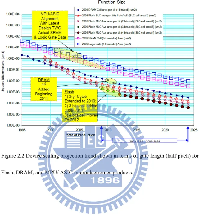
According to Moore's Law [17,18], “the number of transistors that can be placed inexpensively on an integrated circuit(IC) has increased exponentially, doubling approximately every two years“. The future development of integrated electronics or microelectronics depend on the continuous miniaturization allowing more components and more functions to be installed per unit area as shown in Figure 2.1, predicted by 2009 International Technology Roadmap for Semiconductor (ITRS) [19]. Figures 2.2 shows the trend of various device gate lengths scaling, including Flash, DRAM and MPU/ASIC microelectronics products, as predicted by ITRS. However, the continuous feature size shrinking has brought attention to several interconnected issues, such as RC delay, crosstalk noise, and power dissipation. Chapter 2 offers an overview of the development of backend interconnect technology and low-k materials. In addition, the porous low-k materials play an important role in the backend interconnects. The needs, materials, pore generator (porogen) and challenges of ultra-low-k dielectric materials are also briefly reviewed.
2.1 Backend interconnect challenges
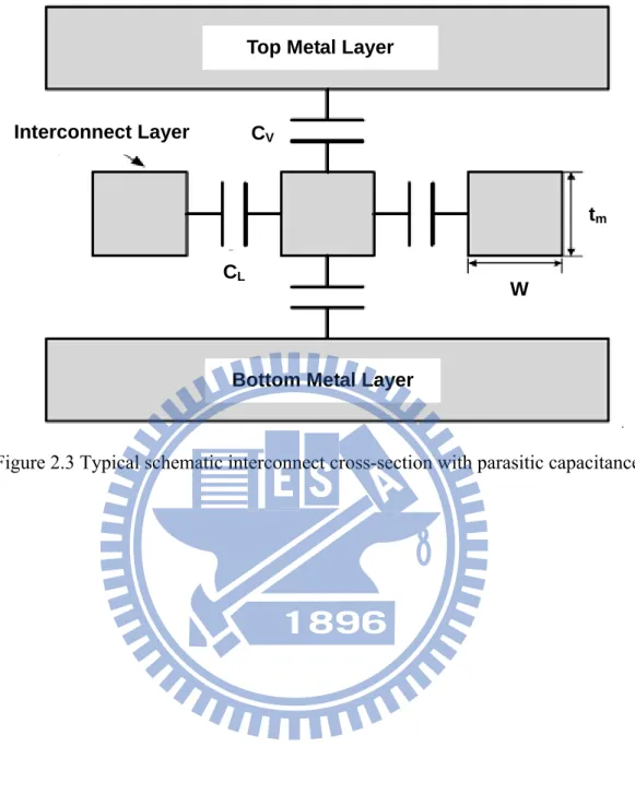
The impact of interconnects scaling can be examined by RC delay of multilevel interconnects. Figure 2.3 shows the typical schematic interconnect cross-section with parasitic capacitance. The size reduction in line and space width of metal enlarges metal line resistance and parasitic capacitance, resulting in serious impact on signal propagation delay and crosstalk noises between metal lines of interconnect. Since one of the major signal delays is associated with interconnect delay, RC delay have become our main concern. Generally, RC delay can be described according to Figure 2.3. By assuming the minimum metal pitch is twice the metal width (W) and the dielectric thickness between the metal lines is the same as the metal height (T), the following equation can be used to predict and calculate the RC delay respectively [20,21].
m m Wt L R (2.1) m m 2 m m V L T W L W t L 2 ) C 2(C C k (2.2) 2 m 2 m 2 2 m t L W L 2 RC k (2.3)
Where R is the resistivity, Lm is the interconnect line length, W is the interconnect line
for achieve higher packing density will lead to the size reduction of W and tm, that will induce higher RC delay. Therefore, according to above RC delay approximation equation, proper improvement of RC delay can be achieved by modification of resistively ( of metal line and relative dielectric constant (k) of inter dielectric layer (ILD). In the early dawn of integrated circuit era, the combination of aluminum (Al) alloys with = 3.3 -cm and silicon dioxide (SiO2, k = 4.0) dielectric has been
utilized extensively for interconnect of semiconductor industry. It is because of their mature subtractive dry-etch processes, and for Al interconnect the production compatibility with fabricated device which have no performance issues. Even so, the relentlessly ICs scaling toward smaller geometry size for improvement of higher integration density and higher speed, demands on the introduction of new material and integration. Beyond 250 nm node, Al/SiO2 interconnects system was no longer
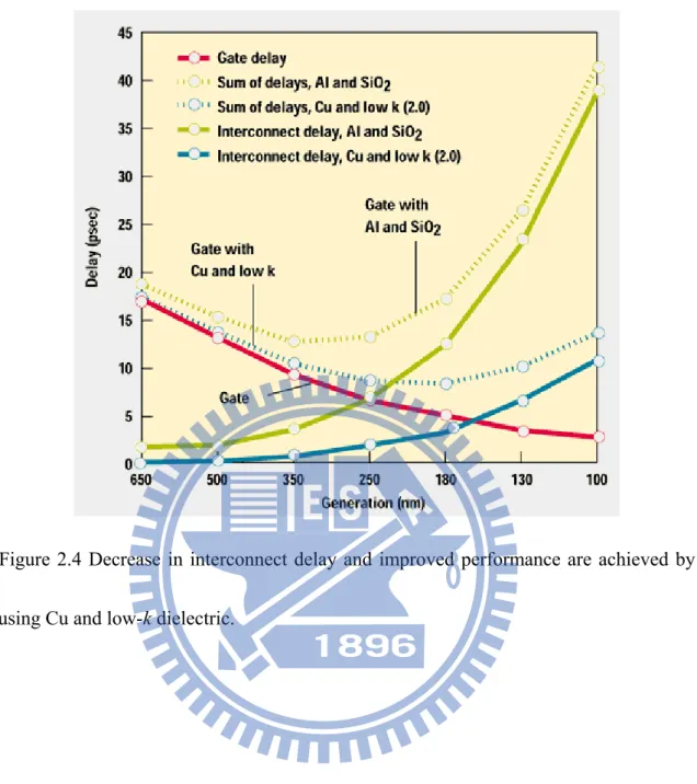
sufficient materials to fulfill the device geometry shrinkage requirement as shown in Figure 2.4 [22]. In order to overcome above mentioned problems, new materials with low resistively and low dielectric constant for use as metal line and ILD materials were urgently studied and developed. Copper (Cu) interconnect was pronounced as one of the most prominent metallization. Cu interconnect is then widely developed due to its low resistively of = 1.9 -cm. Lower interconnect delay is gained from Cu/low-k interconnect system compare to Al/SiO2 interconnect system, utilizing 37 % lower
resistively of copper than aluminum [22]. The capacitance of interconnect is dominated by line-to-line capacitance. Therefore, lowering dielectric constant (capacitance) was indeed crucially needed after the implementation of copper metallization.
The copper dual damascene process has been extensively adopted in the production line, but no consensus exists about the preferred IMD material for 22 nm technology node and beyond. In fact, the implementation of backend interconnect with a required effective dielectric constant (keff), which involves the k-values of dielectric, barrier, and
etchstop layer and their respective dimension (thickness, width), was continuously revised and relaxed by ITRS year to year as shown in Figure 2.5 [23]. In recent years, some of integration strategies and materials development have been proposed to further reduce the keff smaller than 2.0, such as air-gap [24], carbon nanotubes [25], and
graphene nanoribbons [26]. However, it is not easy to successfully integrate these new materials in the near-term because the industry has to radically change the conventional integration and process modules of backend interconnect. In addition, according to the 2010 ITRS, IMD materials with a bulk dielectric constant (kbulk) ≤ 2.2 are expected to be
used in 2013. So far, the manufacturability solution for 20 nm and beyond is not clear. Therefore, the search for low-k materials with kbulk < 2.2, or even < 2.0, is imperative
for semiconductor industry and academia. This study focuses on the reducing of ILD
and while maintaining the conventional backend interconnect processes.
2.2 Classification of dense low-k materials
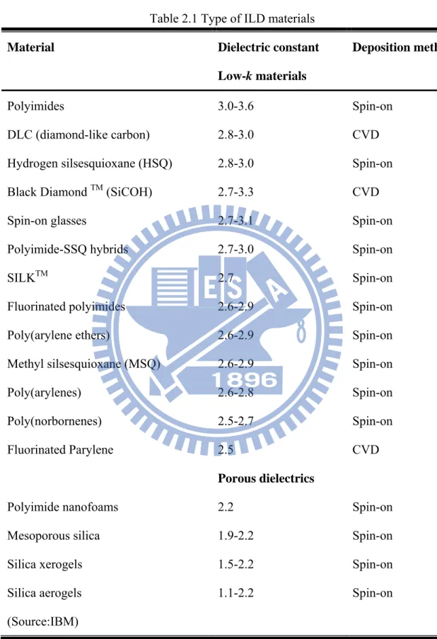
Generally, the major deposition techniques for formation of ILD are divided into primary chemical vapor deposition (CVD) also known as “dry” process which has been widely adopted by chip manufacturers and showed highly reliable. The second one knows as “wet” process called spin-on method which has not been greatly developed in the process. There are some trade-off between CVD method and spin-on method. Spin-on process simply involves the coating of liquid/viscous precursor on the substrate before final curing to remove the solvent. It provides planarizing property that shows in a smoother surface which is highly desirable, and the cost is cheaper. Table 2.1 listed the CVD and spin-on of various ILD materials with their dielectric constant value. Compare to CVD method which involves various gases flow and deposit on the substrate even though it also provides better conformal coverage of the topography, the spin-on method benefit on cleanliness and minimal waste production. Therefore, the spin-on method was selected to study the structure-property relationship of novel low-k materials in this dissertation. Then, next section will introduce the some of potential low-k materials.
2.2.1 Fluorinated Silicate Glass
The fluorinated silicate glasses (FSG) invented by Novellus System Inc and the FSG has dielectric constant value as low as k=3.6. FSG posses lower dielectric constant than SiO2 due to incorporation of fluorine into SiO2 matrix film. Fluorine incorporation
leads to a less dense, more porous film by creating voids in the SiO2 matrix. Typical
FSG film matrix shows in Figure 2.6. Replacing Si–O in the SiO2 matrix with Si–F
reduces the polarizability of the matrix. The above reasons contribute to a lower dielectric constant of the FSG dielectric layer. [27, 28] FSG film has some drawback, for instance SiOF film is hydrophobic, in the meantime the fluorine atom will tend to react with hydrogen atom from water absorb in the release of HF moisture when heated to elevate temperature. The moisture of HF will travel along the interface of ILD and metal causing adhesion become poorer as explained by Figure 2.7. [29]
2.2.2 Carbon-doped Oxide (CDO)
Basically, CDO manage to utilize the chemical vapor deposition (CVD) processing method. CDO low-k is also often designated as SiCOH (carbon-doped silicon oxide). The CDO matrix exists organic bonding such as CH3 backbone that concern lower
polarizability in comparison to Si−O as shows in Figure 2.8. Instead of lower polarizability, CH3 also reduce the density of matrix by induced the matrix steric
hindrance. Regardless of the precursor used, SiCOH can reach k value in the range of 2.4-3. The k-value depends on the number of CH3 groups build into the structure. The
widely studied precursor for SiCOH low-k have been deposited by CVD methods were monometylsilane (1MS), dimethylsilane (2MS), trimethylsilane (3MS), tetra-methylsilane (4MS), Hexamethyldisiloxane (HMDSO), bis-trimethylsilylmethane
(BTMSM), tetravinyltetramethylcyclotetrasiloxane (TVTMCTSO), Vinyltrimethylsilane (VTMS), and tetramethylcyclotetrasiloxane (TMCTS)
[30,31,32,33,34,35,36] as shows in Figure 2.9. CVD CDOs are mainly use in 90nm node. Commercially, the most common CVD OSG materials are AuroraTM (k=2.9, ASM), CoralTM (k=2.85, Novellus), Black DiamondTM (k=2.65-3.0, Applied Materials).
2.2.3 SiLK
TMSpin-coated base SiLKTM was an organic polymer dielectric founded by Dow Chemical in mid 1997. In April 2000, IBM reported the complete integration of SiLKTM dielectric and copper wiring, and announced its intent to commercially fabricate integrated circuits using SiLKTM resin. Toshiba/Sony and Fujitsu also accommodated SiLK resin with hybrid stacks. Aromatic thermosetting polymer SiLKTM with k=2.65 has been proved its compatibility with Cu-dual damascene 0.13 um technology node system [37]. However, the relatively weak mechanical properties (E~3GPa) of SiLKTM
and its poor mismatch of coefficient of thermal expansion (CTE: 66 to 165 ppm/oC) with copper wires and substrates have prevented a wide adoption of SiLKTM in high-volume semiconductor manufacturing. Structure repeating unit of organic SiLKTM shows in Figure 2.10 [38].
2.2.4 Silsesquioxane based materials
Silsesquioxane (SSQ) based low-k material or commonly called T-resin are organic-inorganic polymer with empirical chemical formula (R-SiO1.5)m. The
substituents (R) can include hydrogen, alkyl, alkenyl, alkoxy and aryl. Figure 2.11 illustrates the structure of basic units of SSQ [39]. The contribution of organic substituents benefits in lowering the dielectric constant because they provide lower density of the matrix structure. For the addition, they also attributed to less polarizability organic bond (Si−CH3) compare with Si−O bonds in SiO2. SSQ based
low-k materials is also one kind of organosilicate glasses (OSG) which yield k = 2.5-3.3 after curing step [40,41,42]. The common used SSQ based materials for microelectronic application are mainly hydrogen-silsesquioxane (HSQ) and methyl-silsesquioxane (MSQ). HSQ has hydrogen as a terminal group and MSQ has methyl as a terminal group. The contribution of larger –CH3 group that will cause steric hindrance rather than
possesses less polarization compare to Si–H. Therefore, MSQ material has lower dielectric constant than HSQ material. Table 2.2 summarizes the principle properties of SSQ based dielectric materials compare with SiO2. Subsequently, the commercially
available SSQ based low-k materials are summarized in Table 2.3 which has k < 3.0. [43,44]
2.3 Porous low-k materials
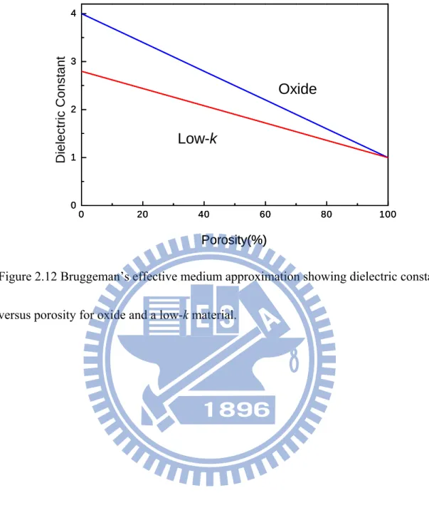
The above mentioned low-k materials were all classified into dense low-k materials. In fact, an ultra-low-k material with k-value ≤ 2.0 is difficult to obtain even though the porosity is increased, and fully densified materials has seemingly reached theirs lowest capability.. Figure 2.12 shows ideal cases for a dry film, which are quite different from typical experimental values [ 45 ]. Therefore, the research has to move on with introduction of porosity into the dense materials, which is the only way to achieve dielectric constants < 2. Pores can be any shapes and morphology, including cylindrical, spherical and plate. Pore size, according to the International Union of Pure and Applied Chemistry (IUPAC) [46], is defined as follows:
Macroporous with dimensions > 50 nm; Mesoporous with dimensions of 2~50 nm; Microporous with dimensions < 2 nm.
The major of porous materials is considered for ILD applications are classified as mesoporous. That is, the average pore size in many candidate porous materials ranges from about 2 to 10 nm. There are two type pore formation inside the dense low-k matrix. The primary one is that pores are inherently formed inside the matrix through sol-gel process such as aerogel and xerogel low-k film. The secondary method of pores formation is though the template agent or pore generator (porogen) which accommodates the present of sacrificial materials that are decomposed upon the thermal process. Following, we will discuss the fact and issue of each porous low-k materials.
2.3.1 Silica aerogel and xerogel low-k dielectrics
SiO2 aerogel thin film has attracted significant attention because of their unique
properties such as ultralow dielectric constant, high porosity, and high thermal stability. SiO2 aerogel thin films usually take the advantage of aging processes. However, SiO2
aerogel thin films usually synthesis above the supercritical pressure (> 60 bar) and high temperature of drying solvent process, which is very expensive and hazardous. Thus, it will become constraint for the production in industrial application [47]. Due to their high porosity, SiO2 aerogel thin film have not display superior mechanical properties
[48]. SiO2 xerogel thin films also employ the same aging technique as SiO2 aerogel thin
ambient drying process which involve pre-drying step that called surface modification process known as silylation. The intention of silylation process is to change the surface hydroxyl (−OH) groups into inert methyl (−CH3) groups. This procedure ensure the film
absorb minimal moisture from the environment [49]. Both SiO2 xerogel and aerogel has
been reported to reach k-value < 2 at porosity level of 70~90% [50,51,52,53].
2.3.2 Pure Silica-Zeolite low-k film
PSZ low-k film offers several advantages over amorphous silica including crystalline structure as well as intrinsically uniform and small pore size [54,55]. Typical PSZ materials have high modulus and low dielectric constant, but have challenges such as high surface roughness [56], which can be resolved by adding a chemical mechanical polishing step. The other major problem is the high moisture absorption of PSZ film [57,58]. This is disadvantageous for the practicability of PSZ film due to the k-value of water is close to 80. Therefore, there have been some efforts to overcome this problem, for example, by performing fluoro-organic functionalization or silylation using 1H,1H,2H,2H-perfluorooctyltriethoxysilane, 3,3,3-trifluoropropyltrimethoxysilane [59], trimethylchlorosilane (TMCS), hexamethyldisilazane (HMDS) [ 60 ], and/or methyltrimethoxysilane (MTMS) during the zeolite synthesis and/or during heating processes to make the surface more hydrophobic [61,62].
2.3.3 Nano-Clustering Silica (NCS)
A novel pore forming method based on spin-on nano-clustering silica (NCS), schematically illustrated in Figure 2.13 [63]. The nano-clustering silica, a MFI-type zeolite film was prepared by sol-gel method. NCS precursor prepared by mixing main matrix of silica source tetraethoxysilane (TEOS) as a soldier in the existence of organic structure directing agent such as tetrapropylammonium hydroxide (TPAOH) as a commander in the present of appropriate solvent such as ethanol. The hydrophobicity of the surface of precursor was modified by adding alkoxysilane (AS) such as methyltrimethoxysilane (MTMS) as a component of the matrix. The difference between pure zeolite low-k and NCS is the addition of methyl (−CH3) groups directly into the
precursor.
2.3.4 Templated-type (porogen) low-k dielectrics
Furthermore, the incorporation of thermally-labile pore generator also can produce porous low-kthin film. The removal of porogen upon high temperature heating will be replaced by pores inside the matrix. First method, incorporation of porogen into the low-k matrix can be accomplished by simply dispersing or mixing the porogen into the solution of low-k precursor [64,65,66]. Porogen size determines the final pore size that
exists inside the matrix. Percentage of porogen added or also called porogen loading determines degree of porosity inside the final cured matrix [67,68]. However, during thermal heating process, the random distribution of pores tends to agglomerate and coalescence which cause a burden to the mechanical strength of final low-k film especially when the porogen loading is increased as shown in Figure 2.14 [69,70].
Recently studies have shown that various polymers could be applied in the SSQ based matrix to form more ordered pore size and pore shape with narrower pore size distribution will be described in Section 2.4.
2.4 Selection of porogens
2.4.1 Linear amphiblic block polymer
Regarding to their ability to self assembly and form micelle as showed in Figure 2.15 [71], block copolymers have become one of the promising candidates for low-k dielectric. Amphibilic di-(or tri-) block copolymer such as PEO-b-PPO-b-PEO [71], PS-b-PEO [72], PS-b-P2VP [73], PS-b-P4VP [18], etc have been studied widely. However, these polymers exhibit very limited miscibility with MSQ precursors, which results in severe phase separation depending on their loading levels, and in large, interconnected pores in cured MSQ dielectrics. However, with increases in the porosity, the pore size increases and thepore size distribution broadens, indicating that the
generated pores change from closed-cell structures to interconnected bicontinuous structures, which is attributed to changes in the phase separation of the blends of the porogen and matrix components with changes in the blend composition [74]. The pore size and size distribution are also found to be affected by the numbers of hydroxylsilyl and alkoxysilyl groups in the PMSSQ precursor. Moreover, neutron reflectivity measurements on these porous films found localized higher porosities at the interface between the porous films and their silicon substrates [75].
2.4.2 Dendrimers polymer
Dendrimers possess three distinguishing architectural components an initiator core, interior layers, and terminal end groups [76,77], and consist of a well-defined, highly branched, compartmentalized structure that is spherical in shape and of nanometre scale. However, both dendrimer porogens and dielectric materials must meet the following requirements if they are to be used to successfully fabricate low-k dielectrics containing closed nanopores. Firstly, the dendrimer porogen should thermally degrade at temperatures lower than the degradation temperature of the dielectric material. Secondly, the dielectric material component must be dimensionally stable or become dimensionally stable during the thermal processes required to burn out the dendrimer porogen component from the dielectric film and in the fabrication of ICs. Thirdly, the
dendrimer and dielectric components should homogeneously dissolve in a mutual solvent without any phase separation. Fourthly, the components must be highly miscible to prevent or minimize any unfavorable phase separation during film formation processing, i.e., solution casting and subsequent drying processes. Finally, both the dendrimer and dielectric components must retain their miscible state without any unfavorable phase separation until the dendrimer porogen is thermally burned out during the post-thermal processing of the dried film, at which point the imprints of the dendrimer molecules are created as nanopores in the resulting dielectric film. The dendrimers were found to be miscible with the PMSSQ precursor, and their sacrificial thermal decompositions result in closed, spherical nanopores in the cured PMSSQ dielectric thin films as showed in Figure 2.16 [78].
2.4.3 Star-shape polymers
Star-shape polymers are very attractive as porogens for imprinting closed nanopores in dielectrics because of their spherical shape in the nanometre size range. Some aliphatic star-shape polymers that completely decompose at temperatures < 400oC even in an inert atmosphere have been reported, such as star shape poly(e-caprolactone)s (PCLs) [79, 80, 81] as showed in Figure 2.17. Among the star-shape polymers PCLs have been extensively investigated for use as porogens in
SSQ dielectrics because of the following chemical characteristics. PCL polymers consist of non-polar pentylenyl and polar ester segments in each repeat unit in the backbone. In addition, they have hydroxyl groups at their arm ends. The PMSSQ dielectric precursor contains hydroxysilyl and alkoxysilyl groups. The PCL polymers are therefore likely to be miscible with the MSQ precursor. Star-shape PCLs with 4–48 arms have been reported. By increasing porosity, star-shape PCL porogens have a tendency to aggregate that is worsened by the cross-linking of the MSQ precursor matrix. Other star-shape porogens exhibit similar problems [82].
2.4.4 Cage supramolecules
Cyclodextrins (CDs) are cyclic oligosaccharides consisting of at least six glucopyranose units joined together by an a-linkage: a-cyclodextrin (α-CD) (6 glucose units), b-cyclodextrin (β-CD) (7 glucose units), and c-cyclodextrin (γ-CD) (8 glucose units) (Figure. 2.18) [83,84]. They are composed of a hydrophobic interior and a hydrophilic exterior; in particular, the hydrophilic exterior may produce favorable interactions with dielectric materials with polar characteristics. These aliphatic compounds are thermally labile cage supramolecules with a maximum diameter of 1.5–2.0 nm. However, the loadings of > 50 wt% were also found to generate wormlike and interconnected pores, as observed for the porous silicates imprinted with CDs.
2.4.5 Well-dispersion porogen
Every porogne will meet a large issue is the aggregation in the hybrid film. Recent studies demonstrated that significant porogen diffusion and aggregation occurred under slow curing condition and resulted in larger porogen size in the MSQ/porogen hybrid film [85]. The rapid curing rate could achieve smaller porogen size and tighter distribution by rapidly forming a cross-linked low-k matrix to freeze up porogen aggregation sterically. But the rapid curing method also lead to residual stress in the porous thin film [86]. Thus, the dispersion of porogen and its impact on the aggregation behavior of porogens prior to the formation of a cross-linked low-k matrix are interested. The huge amount of research concerning particle dispersion in colloids shows thatthe state of the dispersion can be modified, for example, by a highly charged, sterically stabilized polymer and pH value to obtain a high-stability dispersion with the electrostatic and steric effect [87,88,89,90,91]. In this study, we will report the well-dispersion porogen in the solution and hybrid low-k films.
2.4.6 Reactive polymers
The special approach as reactive-porogen method has been proposed to overcome the aggregation of porogen. The reactive porogen were grafted on the low-k matrix
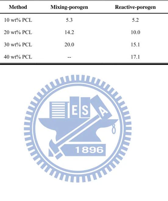
during synthesized scheme by using the sol-gel reaction [92] or atom transfer radical polymerization (ATRP) [93] as showed in Figure 2.19. This method can control the position of porogen in the hybrid film. During processing and film formation, it is also critical that phase separation between the porogen and the low-k matrix occurs during vitrification and that the size scale of kinetic phase separation be limited. On the other hand, the pore size is controlled in the porous film due to the porogen can not diffuse and aggregate in the hybrid film. In general, the grafted porogen will form the small and uniform pore size in the porous film after removal process [93]. Yet, the disadvantage of reactive-porogen method is a complicated scheme for forming the hybrid low-k film and the porogen can not be grafted fully at low-k matrix. There are large numbers un-grafted porogen in the hybrid film causes the porous film hard to appear high porosity (typical ≤ 20 vol.%) [94,95]. For example, the loading of PCL porogen mixing in the matrix from 10 to 20 wt%, the pore sizes are ranging from 5.3 to 14.2 nm. On the other hand, the reactive-poregen PCL of 10 and 20 wt% loading is grafted on the MSQ matrix, the pore sizes are ranging from 5.2 to 10.0 nm. That indicates the reactive-porogen will form smaller pore size than the mixing process. When the loading of reactive-porogen PCL rises to 30~40 wt%, the pore size will range from 15.1 to 17.1 nm. The results show the reactive-porogen is also occurs the aggregation by increasing porogen loading due to the porogen can not be grafted fully at low-k matrix as
summarize in the Table 2.4 [10]. In addition, Table 2.5 shows the characteristics of the other reactive-porogen on MSSQ based low-k material.
2.5 Challenges in porous low-k
As reviewed above, there are two principal methods for producing the templated-type (porogen) low-k dielectric materials containing closed nano-pores, which are the most promising inter dielectric layers for the production of advanced ICs by the semiconductor industry. One method is the mixing of porogen and matrix in solvent to form the precursor and hybrid low-k film. The second is chemically linking the relative-porogens to the network polymers as block components of the backbone or through grafting. Finally, the porogen template approach requires that the dielectric matrix film has a higher degree of cross-linking so that it is dimensionally stable when the pores are created. The porous structure is therefore affected by any further processes associated with the resulting nanoporous dielectric film; this is why silicate and organosilicate precursors and their cured dielectrics are appropriate for the porogen template approach to producing low-k nanoporous dielectrics. Thus, the study focus on the SSQ based materials as dielectric matrix. Because of the reactive-porogen method is too complicated and hard to deliver high porosity (typical < 20 wt% loading of porogen); the mixing process of porogen and matrix is paid close attention in this study.
However, there are some practical requirements if these relationships between the sacrificial porogens, imprinted pores and porosity are to be maintained. Firstly, the sacrificial porogen should be compatible with the dielectric matrix material in order to avoid porogen aggregation. Secondly, the sacrificial porogens should be uniformly distributed throughout the film volume in order to avoid the coalescence or interconnection of the pores.
2.5.1 Pore size
Porous materials will pose even greater challenges to both characterization and integration. Some key material properties directly related to integration issues include pore size, distribution and structure. The average pore size in a low-k porous dielectric layer film must be smaller than the smallest device feature; the minimum metal feature size is nowadays approaching 22 nm and may reach 13 nm in the near future. The pore size distribution (uniform vs. random) may affect the mechanical property of the low-k film. Mechanically, the low-k layers must be strong enough to endure at least the CMP process. The elastic modulus, hardness must be high enough to prevent cohesive failure, cracking or delamination. The minimum requirement of modulus for pass the CMP process is 4 GPa, and hardness has to be larger than 0.5 GPa [96]. An isolated pore structure is often preferred to interconnected pore structure since interconnected pore
may create leakage current paths [97] and have an adverse effect on the mechanical strength. In past paper, the density of the elastic strain energy increases as the pore size decreases. On the other hand, the effective bulk elastic modulus of nanoporous structures with small pore size is larger than that of nanoporous structures with large pore size [98]. Thus, the smaller pore size plays an important role in the porous low-k film. In this study, the post-integration porogen removal approach is proposed to form the porous low-k film. The property of hybrid low-k film will be discussed due to the pore size, distribution, and structure depends on the porogen behavior in the hybrid film before burning out. We will introduce the basic porogen behavior in next section.
2.5.2 Porogen dispersion
However, the pore size was affected significantly by porogen size in the precursor and hybrid film before burning out step. The diffusion and aggregation of porogen will form many large mass in the hybrid film and later larger pore in the porous film. The mixed system of low-k precursor contains the matrix, porogen, and solvent. A homogeneous and uniform solution is recommended a well low-k precursor. The solvent evaporates from the precursor with increasing temperature in which that may be causes the phase separation of porogen and matrix. Significant porogen aggregation occurs in this tern due to the porogen diffuse in the incomplete cross-linking matrix. The isolated
porogen polymer regarded as a nano-particle, and porogen will diffuse and aggregate in the system. In general, the forces of inter-particle including attraction or repulsion will affect the behavior of the particle as showed in the Figure 2.20. There were the repulsive force (VR) and attractive force (VA) between two particles. The VR indicates the
electrostatic forces and streic effect, and that lead particles to exclude the other particles. On the contrary, the VA indicates the van der waals force, and that lead particles to
attract each other [99,100,101]. When two particles approached each other from infinite space, the energy amount (V) could reach to minimum after passing through the energy barrier (Vmax). However, VR is raised will lead Vmax increased and the particles difficult
to approach the other particles. Thus, the increased of electrostatic forces and streic effect can prevent the porogen aggregation. The study will focus on the dispersion of porogen before removal process. A novel method is proposed to increase the electrostatic forces of porogen and control its size in the hybrid film. Finally, that will remain the smaller pore size in the porous film.
2.5.3 Porogen loading and high porosity
According to 2010 ITRS, upcoming 22 nm technology node of IC industry requires dielectric materials with k-value <2.3, which requires an increase in free volume by incorporating porosity through nanoporous pores, as well as a reduction of polarizability.
For example, for a dense materials such as MSQ (k~2.9), a high porosity, ~60% is required in order to obtain an ultra-low-k porous MSQ of k~2.0. In the porous low-k films, the porosity is critical parameter controlling the dielectric constant, mechanical strength, and stress. Moreover, small and isolated pores with a tight pore size distribution are highly desired in order to achieve better mechanical strength and better barrier reliability because a conformal and continuous barrier can be formed onto such a porous low-k film [102].
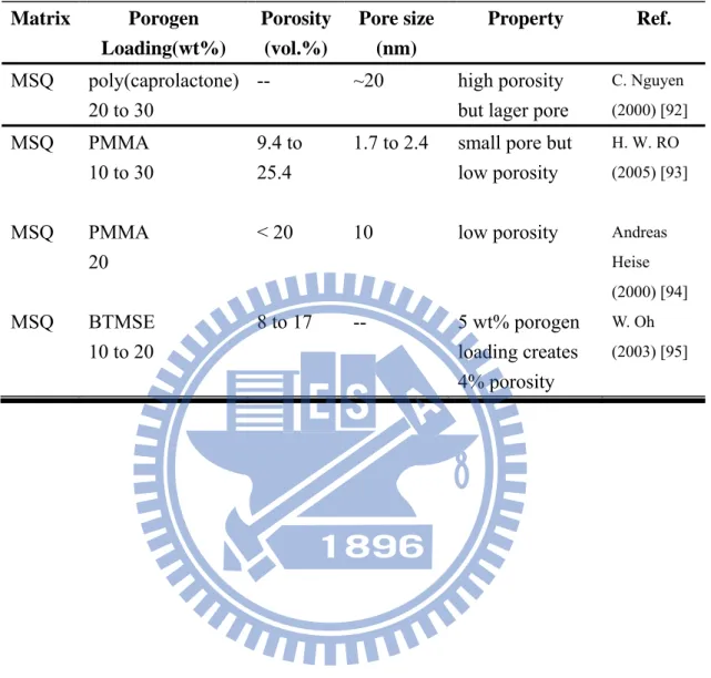
However, there is huge challenge in maintaining the pore size without aggregation or forming interconnected pores at high porosity. Many studies show that the pore size increases and pore shape becomes interconnected or elliptic with increasing porosity (or porogen loading) in the low-k porous film [103,104]. Larger or interconnected pores at high porosity can significantly reduce the mechanical strength of porous low-k film [71,105]. In addition, closed nanopore can be obtained, within certain boundary conditions related to the nature and total load of the porogen as summarized in the Table 2.5 [71,79,105, 106 , 107 , 108 , 109 , 110 , 111 ]. The past study indicate the obvious aggregation of pore at porogen loading > 25% and focus on the property of low-k porous film with porosity < about 30 vol.% [69]. In this study, the porogen surface modification by ionic surfactant will be used to disperse porogen in the hybrid low-k system. In addition, the porogen loading (or porosity) is also increased in the system.
The property of pore at high porosity (>30 vol.%) and the critical (or ideal) porosity with no-aggregated pore will be discussed.
2.6 Post-integration porogen removal scheme
The novel post-integration porogen removal approach, which detail integration scheme is illustrated in Figure 2.21, has been proposed based on material design and integration scheme to circumvent the reliability issues of porous dielectrics mentioned previous section. Malhouitre et al. [112] and Fayolle et al. [113] have demonstrated that such novel material and scheme could be achieved in a copper single damascene structure with a 25% RC reduction after porogen removal. Recently, post-integration porogen removal approach has been applied to reduce the plasma-induced damage to porous low-k dielectrics because porogen can reduce effective pore size and limit the plasma radical diffusion inside pore [14,15]. For such a scheme, the decomposition temperature (Td) of high-temperature porogen candidates needs to be higher than the
maximum processing temperature (> 350oC) with the post-integration porogen removal scheme [114]. Moreover, the mechanical strength of hybrid low-k material should be strong enough to pass all of the backend processing steps, especially the chemical-mechanical polish (CMP) step. On the other hand, for such hybrid dielectrics or its porous form, there are additional concerns relate to moisture uptake induced by
processing steps such as CMP, post-etch cleaning, post-CMP cleaning or resist removal [115,116,117]. Therefore, the structure-property relationship of hybrid low-k materials using in the post-integration porogen removal scheme will be further studied in this dissertation.
The thermal stability of the porogens used in the as-deposited porous low-k film are typically not so high such that porogens can be removed readily to form porosity during dielectric deposition or subsequent thermal treatment. As for the high-temperature porogens in the late porogen removal scheme, it is desirable to attain a high and sharp decomposition temperature by incorporating stable structures such as aromatic rings or double/triple bonds as well as by using similar moieties in a block copolymer. For example, polystyrene-b-polybutadiene-b-polystyrene (SBS) and polystyrene (PS) could be chosen as a good high-temperature porogen candidate due to its similar aromatic structure which can provide a good thermal stability and desired decomposition temperature. The study focus on the porogen surface modification by using ionic surfactant, and the thermal stability of surfactant is required to consider.
Material Dielectric constant Deposition method
Low-k materials
Polyimides 3.0-3.6 Spin-on
DLC (diamond-like carbon) 2.8-3.0 CVD Hydrogen silsesquioxane (HSQ) 2.8-3.0 Spin-on Black Diamond TM (SiCOH) 2.7-3.3 CVD Spin-on glasses 2.7-3.1 Spin-on Polyimide-SSQ hybrids 2.7-3.0 Spin-on
SILKTM 2.7 Spin-on
Fluorinated polyimides 2.6-2.9 Spin-on Poly(arylene ethers) 2.6-2.9 Spin-on Methyl silsesquioxane (MSQ) 2.6-2.9 Spin-on
Poly(arylenes) 2.6-2.8 Spin-on
Poly(norbornenes) 2.5-2.7 Spin-on
Fluorinated Parylene 2.5 CVD
Porous dielectrics
Polyimide nanofoams 2.2 Spin-on Mesoporous silica 1.9-2.2 Spin-on Silica xerogels 1.5-2.2 Spin-on Silica aerogels 1.1-2.2 Spin-on
(Source:IBM)
Property MSQ HSQ SiO2
Dielectric Constant 2.8 3.0 4.0
Modulus (GPa) 3-5 6 59
Density (g/cm3) 1.2-1.3 1.4-1.5 2.4 Tensile Strength (MPa) 50 80 -
Material Trade Name k-value Company HSQ FOx (flowable oxide) 2.9-3.0 Dow Corning
MSQ RZ25-15 2.6 Hitachi
MSQ HOSP 2.6 Honeywell
Porous HSQ XLK 2.2 Dow Corning Porous HSQ LKD 5109 2.2-2.3 JSR Porous MSQ Zirkon 2.3 Shipley
Method Mixing-porogen Reactive-porogen
10 wt% PCL 5.3 5.2
20 wt% PCL 14.2 10.0
30 wt% PCL 20.0 15.1
40 wt% PCL -- 17.1
Matrix Porogen Loading(wt%) Porosity (vol.%) Pore size (nm) Property Ref. MSQ poly(caprolactone) 20 to 30 -- ~20 high porosity but lager pore
C. Nguyen (2000) [92] MSQ PMMA 10 to 30 9.4 to 25.4
1.7 to 2.4 small pore but low porosity
H. W. RO (2005) [93]
MSQ PMMA 20
< 20 10 low porosity Andreas Heise (2000) [94] MSQ BTMSE 10 to 20 8 to 17 -- 5 wt% porogen loading creates 4% porosity W. Oh (2003) [95]
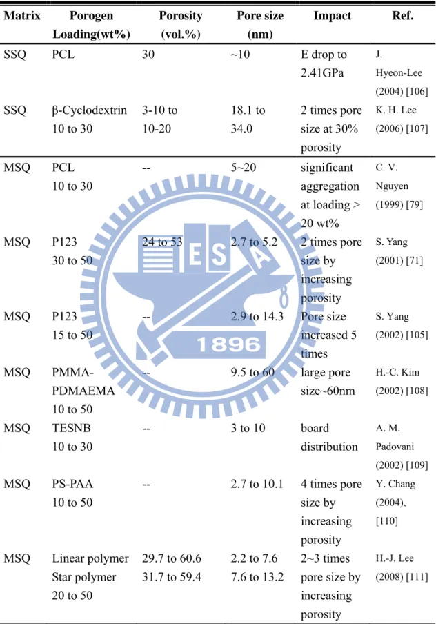
Matrix Porogen Loading(wt%) Porosity (vol.%) Pore size (nm) Impact Ref. SSQ PCL 30 ~10 E drop to 2.41GPa J. Hyeon-Lee (2004) [106] SSQ β-Cyclodextrin 10 to 30 3-10 to 10-20 18.1 to 34.0 2 times pore size at 30% porosity K. H. Lee (2006) [107] MSQ PCL 10 to 30 -- 5~20 significant aggregation at loading > 20 wt% C. V. Nguyen (1999) [79] MSQ P123 30 to 50 24 to 53 2.7 to 5.2 2 times pore size by increasing porosity S. Yang (2001) [71] MSQ P123 15 to 50 -- 2.9 to 14.3 Pore size increased 5 times S. Yang (2002) [105] MSQ PMMA- PDMAEMA 10 to 50 -- 9.5 to 60 large pore size~60nm H.-C. Kim (2002) [108] MSQ TESNB 10 to 30 -- 3 to 10 board distribution A. M. Padovani (2002) [109] MSQ PS-PAA 10 to 50 -- 2.7 to 10.1 4 times pore size by increasing porosity Y. Chang (2004), [110] MSQ Linear polymer Star polymer 20 to 50 29.7 to 60.6 31.7 to 59.4 2.2 to 7.6 7.6 to 13.2 2~3 times pore size by increasing porosity H.-J. Lee (2008) [111]
Figure 2.2 Device scaling projection trend shown in terms of gate length (half pitch) for Flash, DRAM, and MPU/ ASIC microelectronics products.
Figure 2.3 Typical schematic interconnect cross-section with parasitic capacitance
Top Metal Layer
Bottom Metal Layer CV
CL
W
tm Interconnect Layer
Figure 2.4 Decrease in interconnect delay and improved performance are achieved by using Cu and low-k dielectric.
Figure 2.6 Basic structure of FSG matrix.
O
Si
O
Si
Si
Si
Si
Si
O
O
O
O
O
F
F
Figure 2.7 Depiction of possible bond rearrangements upon SiOF film hydration to produce Si−OH bonding and the release of HF from the film.
Si
O
O
O
Si
O
O
O
O
H
H
F
Si H CH3 H H Si H CH3 H3C H Si H3C CH3 H CH3 Si H3C CH3 H3C CH3 (a) 1MS (b) 2MS (c) 3MS (d) 4MS Si O Si O Si O Si O CH3 H H H3C H H3C H CH3 Si O Si O Si O Si O CH3 H H H3C H H3C H CH3 (e) TMCTS (f) OMCTS Si H3C OCH3 H3C OCH3 Si H3C OCH2CH3 H3C OCH2CH3 (g) DMDMOS (h) DEMS
Figure 2.11 Basic structure units of SSQ dielectric materials consist of random, ladder and cage structures. R= H, CH3 for HSQ and MSQ respectively.
0 20 40 60 80 100 0 1 2 3 4 Porosity(%) 0 20 40 60 80 100 0 1 2 3 4 0 20 40 60 80 100 0 1 2 3 4 Porosity(%) D iel ectr ic C o nst a nt
Oxide
Low-k
Figure 2.12 Bruggeman’s effective medium approximation showing dielectric constant versus porosity for oxide and a low-k material.
Figure 2.13 Schematics of the nano clustering silica (NSC) formulation and its film deposition and curing processes.
Figure 2.14 The conventional formation of porous low-k by using template-type porogen method.
Figure 2.15 Schematic structures of phase behaviors of PEO-b-PPO-b-PEO triblock copolymers in MSQ matrixes.
Fig. 2.16 Procedure for preparation of a nanoporous organosilicate dielectric thin film from a curable polymethylsilsesquioxane precursor matrix and a thermally labile globular dendrimer porogen (EA-PPI-64 or EA-PPI-128).
Fig. 2.17 Star-shape polymer porogens: PCL4, four-armed poly(ecaprolactone) and PCL6, six-armed poly(e-caprolactone).
(a)
(b)