Contributed Paper
Manuscript received 04/15/12 Current version published 06/22/12
Electronic version published 06/22/12. 0098 3063/12/$20.00 © 2012 IEEE
High Efficiency Data Access System Architecture for Deblocking
Filter Supporting Multiple Video Coding Standards
Cheng-An Chien, Guo-An Jian, Hsiu-Cheng Chang, Kuan-Hung Chen, Member, IEEE,
and Jiun-In Guo, Member, IEEE
Abstract — This paper presents an efficient VLSI architecture
of in-loop deblocking filter (ILF) with high efficiency data access system for supporting multiple video coding standards including H.264 BP/MP/HP, SVC, MVC, AVS, and VC-1. Advanced standards, such as H.264 MP/HP, SVC, and MVC, adopt Macro Block Adaptive Frame Field (MBAFF) to enhance coding efficiency which results in the performance bottleneck of deblocking filter due to complex data access requirement. This design challenge has not been discussed in previous works according to our best knowledge. Therefore, we develop a Prediction Data Management (PDM) to manage the input prediction data order of deblocking filter for different coding types (like frame/field) and multiple standards. We also design an extended output frame buffer module to solve the system bus architecture restriction (like 1K boundary and burst length) and achieve high efficiency data access by using MB-based scan order. By using these techniques, we can solve the data accessing design challenge and reduce 67% bus latency. After being implemented by using 90 nm CMOS technology, the proposed work can achieve real-time performance requirement of QFHD (3840×2160@30fps) when operated at 156MHz at the cost of 50.6K gates and 2.4K bytes local memory. The maximum operating frequency of the proposed design, i.e. 370MHz, is higher than the required real-time operating frequency so that voltage scaling may be adopted to reduce power consumption. 1
Index Terms —High efficiency, Deblocking filter, Multiple video standards
I. INTRODUCTION
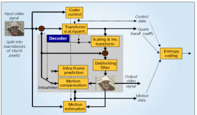
Deblocking filter plays an important role in current video coding applications, including MPEG4, H.264, SVC, MVC, AVS, and VC-1 and so on. Similar to MPEG, each standard adopts a transform-based coding with quantization, which induces quantization errors on each block boundary. The deblocking filter is proposed to remove the blocking effect to enhance video quality, especially in low bit rates. Fig. 1 shows the H.264 encoding flow. Since the deblocking filter is in the
1 Cheng-An Chien, Guo-An Jian, and Hsiu-Cheng Chang are with the Computer Science and Information Engineering Department, National Chung-Cheng University, Chia-Yi, Taiwan (e-mail: {cca95m, chienka, changhsc} @cs.ccu.edu.tw).
Kuan-Hung Chen was with National Chung-Cheng University, Chia-Yi, Taiwan. He has joined the faculty of Electronic Engineering Department, Feng-Chia University, Tai-Chung, Taiwan (e-mail: [email protected]).
Jiun-In Guo is a professor with the Electronics Engineering Department, National Chiao-Tung University, Hsin-Chu, Taiwan (e-mail: [email protected]).
encoding loop, it is also called in-loop deblocking filter. In order to deal with the high quality video applications in HDTV, there are some new coding tools introduced in H.264 main profile (MP)/ high profile (HP) protocol for deblocking filter, including Macro Block Adaptive Frame/Field (MBAFF) coding and 8x8 transform, which not only improve the coding quality, but also complicate the realization of deblocking filter. SVC and MVC are extended video standards from H.264 HP for supporting scalable and multi-view video, equipped with the same deblocking filter as H.264 HP. Besides H.264, the deblocking filter is also used in other coding standards like VC-1 and AVS. VC-1 [15] is a video codec specification that has been standardized by the Society of Motion Picture and Television Engineers (SMPTE) and is adopted in next-generation optical media applications. The deblocking filter in VC-1 is an in-loop filter arranged by frame-based orders, which means that all the horizontal edges should be filtered first and then followed by the filtering of vertical edges. In addition, Audio Video Coding Standard (AVS) is a video codec specification that has been standardized by China. The AVS deblocking filter presents an 8x8 edge filter with the same filter order as that in H.264. Similarly, it has two modes for filtering. Therefore, a high-performance deblocking filter architecture with flexibility to support multiple video coding standards is inevitable.
Fig. 1. H.264 Encoding Flowchart
Recently, there are many researches involved in designing the deblocking filter architectures [3]-[14]. All of them only supported a single standard and a single profile decoding. Among the H.264 baseline profile (BP) designs [3]-[5], the design [3] used a separate filter method with the original filter order defined by the standard. It filters all the vertical edges in a MB, and then filters all the horizontal edges. The design [4] used a raster scan order as the filter order to reduce the cycle
counts. Besides, the design [5] proposed a hybrid filter order to reuse the pixel without affecting the data dependency in the original filter order. It eliminated the cycle count for a MB and reduced the intermediate buffer cost. The works [13]-[14] are the H.264 deblocking filter design in recent years which focus on the low power and high efficiency by reducing the processing cycles. All of these previous H.264 deblocking designs support H.264 baseline profile (BP) only. In the VC-1 deblocking filter design [6], a raster scan order is used as the filter order for reducing the cycle count. The design [7] used a RISC architecture for filtering VC-1. Similar to the design [3], the AVS design [8] used a large separate SRAM with the original filtering order defined by the standard. But, it needs additional cycles when the deblocking filter switches the vertical and horizontal edges. Moreover, the design [10] is the first deblocking filter design supporting multiple video standards. It proposed a hybrid filtering order to support the deblocking filters for both H.264 and MPEG4 by using in-loop filter of H.264 to realize post-loop filter of MPEG4. Most of these reference designs only can process small resolution videos, e.g. the QCIF (176x144), due to limitation of their local memory size. If higher resolution videos are demanded, it is necessary to increase their local memory size.
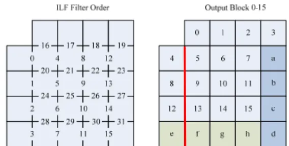
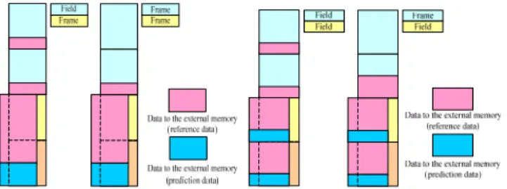
In these designs [3]-[14], they did not mention about how the debolcking filter accesses the input data and writes out data. Most of these previous designs use the testbench to process the input and output data. Fig. 2 shows the filter order defined in H.264 standard and the filtered data after one MB deblocking (i.e. block 0-15). Since the bottom and right 4x4 block rows (i.e. block a-h) are used in deblocking filtering of next MB, these 4x4 blocks cannot be written out to the external memory together with all the other blocks in hardware implementation. For writing out the filtered data in one MB, we need to use 16 write commands at least by using INCR4 in AHB 2.0 protocol with bus latency per command. If the data written to external memory address cross the 1K boundary, one write command needs to be separated into two commands, as denoted by the redline shown in Fig. 2. Therefore, we propose an output frame buffer to collect the filtered data into one complete MB before writing data out. It can avoid the cross 1K boundary problem. We also support the MB-based write out order in encoder to reduce write commands as well as bus latency. By using the MB-based scan order output frame buffer, we can reduce up to 67% bandwidth.
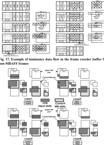
For supporting up to SVC/MVC/H.264 MP/HP coding tools, there are design challenges to be overcome. The major one is how to support the MBAFF tool when doing in-loop filtering (ILF). The MBAFF tool uses MB-pair structure in the encoding flow, which induces high complexity in H.264 decoding. Fig. 3 shows the H.264 MBAFF coding flow using MB-pairs. In Fig. 3, when decoding the current MBs, we need the reference information from the upper and left MBs that may be encoded in different MB frame or field modes. In this way, the complexity to arrange these reference data would become higher than that in H.264 BP, as indicated in Fig. 3. Therefore,
we propose a prediction data management (PDM) scheme to process each kind of MB modes in MBAFF. Another challenge is to support the 8x8 transform coding in H.264 HP and AVS. It complicates the deblocking filter order to support both 4x4 blocks and 8x8 blocks at the same time.
Fig. 2. H.264 and AVS Deblocking Filter Order and Write Out Data
In addition to the PDM scheme, we propose two more techniques including shared adder-based algorithm and integrated mode decision algorithm for reducing the local memory to achieve high data throughput rate as well. Encapsulating all of the proposed design techniques, the proposed design has been realized at the cost of 38.4K gates and 672 bytes of local memory when operating at 370MHz, according to the 90nm CMOS technology. Moreover, the proposed design can achieve the data throughput rate of 160 cycles per MB in average, which meets the real-time processing requirement for H.264 quadruple full HD resolution, i.e. QFHD(3840x2160@30fps) video decoding. As compared to the existing designs, the proposed design is the first one presenting efficient realization of deblocking filters which can handle the newly added complex coding tool, i.e. MBAFF for multiple video coding standards. We also propose a extended prediction data buffer (PDB) with the output frame buffer (OFB) which co-works with the proposed PDM to reduce the AHB bus bandwidth by avoiding the cross 1K boundary problem and increasing the burst length for real applications.
Fig. 3. H.264 MBAFF Coding Flowchart
The rest of this paper is organized as follows. In Section II we illustrate the proposed deblocking filter algorithm for each standard. In Section III we present the hardware architecture of the proposed design. In Section IV we show the implementation results and the performance comparison of the proposed design with the existing ones. Finally, conclusion is given in Section V.
672 IEEE Transactions on Consumer Electronics, Vol. 58, No. 2, May 2012
II. PROPOSED DEBLOCKING FILTER ALGORITHM
To support multiple video coding standards, we classify all the deblocking filters into three types, i.e. H.264/SVC/MVC and VC-1 normal MB based on 4x4 blocks without MBAFF, H.264 HP/SVC/MVC and AVS based on 8x8 blocks, and H.264/SVC/MVC MBAFF based on 4x4 blocks, as presented in the following.
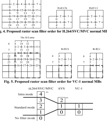
A. Proposed deblocking filter algorithm for H.264/SVC/MVC and VC-1 normal MBs without H.264 MBAFF (4x4 blocks)
All the H.264/SVC/MVC and VC-1 deblocking filters need to filter each edge of 4x4 blocks. As analyzed in the designs [3] and [8], using the raster scan filtering order can reduce more local buffer size and processing cycles. So, we adopt this concept to filter 4x4 edges for normal MBs. Fig. 4 shows the filter order in H.264/SVC/MVC, and Fig. 5 shows the filter order in VC-1 that is different from H.264/SVC/MVC because VC-1 needs to filter 8x8 edges first. Since the AVS is based on the 8x8 transform coding, the filter order for AVS will be described in Section II (B). Before filtering, the H.264/SVC/MVC employs the boundary strength (BS) to denote the strength of the filtering edge for selecting appropriate filters. For example, BS = 0 means no need to filter, BS = 1, 2, 3 means a weak mode filter, and BS = 4 means a strong mode intra filter in H.264/SVC/MVC. Besides, VC-1 can also use a BS value to determine whether filtering is required or not. Hence, we integrate the BS mode decision for multiple video coding standards, as shown in Fig. 6.
Fig. 4. Proposed raster scan filter order for H.264/SVC/MVC normal MBs
Fig. 5. Proposed raster scan filter order for VC-1 normal MBs
Fig. 6. Integrated mode decision for H.264/SVC/MVC, VC-1, and AVS
To realize the deblocking filter operations, we find that there are some common items which can be shared by doing once in hardware for reducing the hardware cost. Moreover, since the deblocking filter for chrominance pixels is almost the same as that for luminance pixels, we can share the data path as well for
filtering luminance and chrominance pixels. Fig. 7 shows the optimization steps of the intra strong filter by sharing the common terms. This method and architecture can be used in each standard. We can also share the same hardware architecture in different standards to reduce the hardware cost. The detailed architecture is introduced in section III (A).
Fig. 7. Shared adder-based algorithm for intra strong filter
B. Proposed deblocking filter algorithm for H.264 HP/SVC/MVC and AVS 8x8 blocks
Both H.264 HP/SVC/MVC and AVS standards adopt 8x8 transform coding where the deblocking filter only filters the 8x8 edges in MBs. Moreover, one 8x8 edge can be divided into two 4x4 edges so that we can share the same filter hardware to process both the 4x4/8x8 edges. We use the same filter order from the normal filter by setting the BS=0 to skip the 4x4 edges. By using this skipping method, we can reduce the processing cycle and power consumption in H.264 HP/SVC/MVC and AVS. Fig. 8 shows the filter order for 8x8 edges.
Fig. 8. Proposed raster scan filter order for H.264 HP and AVS normal MBs
C. Proposed deblocking filter algorithm for H.264/SVC/MVC MBAFF MB pair (4x4 blocks)
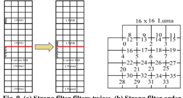
In H.264 MP/HP/SVC/MVC, frame/field MB modes and MBAFF are supported. The filtering algorithm is the same as the 4x4 blocks we mentioned in section II (A). There are four cases between the reference MB-pair and the current one, which can be classified as frame/frame, frame/field, field/frame, and field/field between the upper and current MBs, as shown in Fig. 3. These cases are also happened between the left and current MBs. There is a strong filter in MB boundary on which the data need to be filtered twice when the upper reference MB-pair is field and the current MB-pair is frame, as shown in Fig. 9(a) and 9(b). We propose a PDM scheme to efficiently process the first horizontal edge twice in strong filtering and other MBAFF cases, which is illustrated in more details in Section III (C).
Fig. 9. (a) Strong filter filters twice; (b) Strong filter order
III. PROPOSED DEBLOCKING FILTER ARCHITECTURE
According to the proposed deblocking filter algorithm, we design the associated architecture, as shown in Fig. 10. Two dedicated SRAMs, illustrated as oblique line regions, are adopted to respectively store the reference data of the upper and left MB-pairs, which ensures an efficient data access for filtering MBAFF MBs. In addition, the proposed in-loop deblocking filter design contains the following components, i.e. a 1-D deblocking filter, two transpose units, and various data buffers. The controller is responsible for the following tasks, like deciding integrated BS values, providing the correct filter mode when filtering each standard, and writing out the filtered data to the output frame buffer. The proposed deblocking filter design with four pipeline stages can filter one MB for 160 cycles in normal MB mode. Another extended module is prediction data buffer (PDB) which contains two buffers and a controller to manage the prediction data and the output data between the ILF and external memory by using AHB interface. The major components of the proposed deblocking filter architecture are introduced in detail in the following:
Fig. 10. Proposed ILF and PDB hardware block diagram with four pipeline stages, where oblique line regions denote local memory
A. Shared Adder-based 1-D Filter
The 1-D deblocking filter module is the filter kernel in the proposed design. It is a 4-pixel edge filter, and realizes the filter operations in different video coding standards according to the BS values. There are two filter operations, including the
intra filter and the standard filter. For intra filter, we find some common shared items that can be shared by doing once in hardware for reducing the hardware cost, as shown in Fig. 7. Since the intra strong filter for chrominance is almost the same as that for luminance pixels, we can share the data path for filtering luminance and chrominance pixels. For standard filter, Fig. 11 shows the shared standard filter architecture in the proposed design. The VC-1 filter formula is very similar to the H.264 standard filter. It needs to filter both the p0 and q0. But different from the H.264, VC-1 needs to use two same formulas to decide the delta value for the p0 and q0. Hence, we combine one formula into H.264’s path and use PE2 to calculate the other formula for VC-1 filtering. It can also share the data-path for doing the luminance and chrominance standard filtering operations. The data-path sharing concept could also be applied to the architecture in intra filter.
1 Reg p3(ap)p2 p1 p0 q0 q1 q2 q3(aq) a0 + >>1 + + <<1 ->>1 clip + MUX q1_o <<1 ->>1 clip + MUX p1_o tc0_table Reg + + + MUX 1 clip PE MUX + p0_reg - q0_reg p0_o q0_o <<1 -<<2 + ~ + >>3 4 MU X MU X Reg MU X >>1 clip clip -tc tc delta 0 255 255 q0 p0 q2 p2 q1 p1 clip tc0 tc0 -tc0 -tc0 aq ap a0 PE2 Reg MUX MU X 0 Reg Reg Reg Reg Delta/p2p1 q1q2 Reg
Fig. 11. Proposed shared standard filter architecture
B. MBAFF Right Buffer
MBAFF right buffer is used to store the rightest 4x4 block column in the current MB, which are used again as reference data for filtering on the next MB. For supporting the H.264 MBAFF and VC-1 coding, we have to store the two 4x4 block rows located at the right side of MB-pair or MB. The right buffer uses a 96x32-bit dual port SRAM which uses a controller to output calculated data with order according to the next MB mode. C. Prediction Data Management (PDM)
According to above H.264 MBAFF algorithm presented in Section II, no matter the current MB-pair is field or frame mode, we have to store two 4x4 block rows to the external memory. Suppose the uncompleted filtered data from the upper MB are stored in external memory as described above, we still encounter order mismatch between the read access from external memory and the reference filter data of top boundary. As a result, there are four cases (frame/frame, frame/field, field/frame and field/field) that we must produce the correct input order for top boundary filter, as show in Fig. 12. We propose the PDM scheme for the four cases of upper MB-pair/current MB-pair as follows.
674 IEEE Transactions on Consumer Electronics, Vol. 58, No. 2, May 2012
Fig. 12. Data written to external memory for different MB-pair modes
a) Frame/Frame Mode
In this case, we adopt a “Preloading Parallel Buffer” scheme to reduce processing cycles and provide the correct reference input for top boundary filter. We use this scheme to get two 4x4 block row data from the upper MB for the current MB pair to filter. For example, if the current MB pair is at (x, y) as shown in Fig. 13, the proposed method starts loading the prediction data from MB pair at (x+1, y-1). Then, if the current MB pair is changed into (x+1, y), the preload buffer will write the upper 4x4 block prediction row at MB pair (x+1, y-1) to reference frame memory through the transpose unit. Then, the reference input of top boundary filter will obtain 4x4 block prediction row at MB pair (x+1, y-1) from PDB at the same time. This scheme is also used in VC-1 mode.
Fig. 13. Proposed “Preloading parallel buffer” scheme
b) Frame/Field Mode
In this case, we adopt a “Mixed Preloading Parallel Buffer” scheme to reorder the prediction data from upper MB-pair. First, preloading is the same as that in frame/frame case in order to store the first eight 4x4 blocks from upper MB-pair. Second, we mix the byte locations from the preload buffer (0, 2) bytes and PDB (4, 6) bytes to provide the correct order for filtering, as illustrated in Fig. 14. Finally, four bytes (1, 3, 5, 7) will be written back to the preload buffer for providing the reference input for top boundary filter of bottom MB. This case can also be used in VC-1 since it also needs to store two rows of 4x4 blocks.
c) Field/Field Mode
This case is easy for implementation because the orders for read access from external memory and the reference filter for top boundary are the same.
Fig. 14. Mixing operation in frame/field mode
d) Field/Frame Mode
As described in Section II, the major reason of adopting different filter orders is to simplify the controller of the preload buffer. Our idea is whether the current MB-pair is in frame mode or field mode, as long as the top MB pair is in field mode, the preload buffer controller will not operate and turn the task into PDB controller. We propose a “Dual Rearrangement Strong Buffer” scheme denoted as DRSB and a “Strong filter order” algorithm in the proposed design. Two 16x32bits FIFOs are used to store the current two 4x4 block rows, and one FIFO is shared with temporal buffer. After filtering edge 7 in Fig. 9 (b), we mix byte position of dual buffer output to apply to filter edges 8~11 in Fig. 9 (b) and restore unfiltered bytes to another buffer. Then, we read bytes 1, 3, 5 and 7 from one buffer in order to apply to filter edges 12~15 in Fig. 9 (b). Eventually, the output of filtering edges 12~15 in Fig. 9 (b) will be mixed again according to the order of byte in turn. Moreover, this byte order (0, 1, .., 7) in DRSB will be applied to filter edges 16~19 in Fig. 9 (b). These steps are shown in Fig.15 (a)-(d) on after filtering each edge.
4 0 1 2 3 5 12 8 9 1011 13 7 6 15 14 4 0 1 2 3 5 12 8 9 1011 13 7 6 15 14
(a) “DRSB” arrangement when finishing filtering edge 7
(b) “DRSB” arrangement when starting filtering edge 8
(c) “DRSB” arrangement when finishing filtering edge 11
(d) “DRSB” arrangement when starting filtering edge 15 Fig. 15. DRSB arrangement processing flow
D. Output Frame Buffer (OFB)
Prediction data buffer (PDB) contains two buffers and a controller to manage the prediction data and the output data. The first buffer is a prediction buffer for getting the upper MB prediction data from external memory. Therefore, the proposed design will not be limited on any targeted resolution and also reduce the local memory size.
The second buffer is output frame buffer (OFB). According to the write out data problem we mentioned in Fig. 2, we use an output frame module in the PDB to resolve this problem. We use this buffer to collect the filtered data into a completed MB for writing out. Fig. 16 shows the block diagram of the proposed OFB. We use four banks to solve different field or frame MB types by interleaving storing the MB data into frame type for display. The proposed frame output buffer includes four SRAMs. The output data of ILF are in 4x4 blocks, but the external memory is connected to a 64-bit data bus. So the data have to be merged to 64 bits before being written out to external memory. Therefore, different banks, i.e. bank0 and bank1, are used for storing the luminance data for top MB, while the bank2 and bank3 are used for storing the luminance data for bottom MB. The data flow is described as follows. First, the 4x4 blocks of data in MB(n) are input and written to the locations with addresses {0, 2, 4, 6} in bank0. Then, the following blocks are written to the locations with addresses {0, 2, 4, 6} in bank1 and addresses {1, 3, 5, 7} in bank0 consecutively. While decoding the MB(n+1), the data are written to the locations with addresses {1, 3, 5, 7} in bank1, and the data in MB(n) are all ready for being written out to external memory. The detailed flow is illustrated in Fig. 17 for luminance data in non-MBAFF frame. As for the chrominance data, the Cb and Cr data also use different banks for being merged from 32 bits to 64 bits data. In addition, the luminance and chrominance data will not input simultaneously. So, the input buffer (SRAM) can be shared to reduce the SRAM size. However, the frame buffer is organized by interleaving Cb and Cr data, which results in that the Cb and Cr data have to be merged to 64 bits before being written out. Therefore, the SRAM is used in different banks of order for accessing the Cb and Cr data simultaneously. The order for Cb data is {bank0, bank1}, and the order for Cr data is {bank1, bank0}. For MBAFF frame decoding, there are four input cases between the current MB pair and upper MB pair, as the OFB input data shown in Fig. 18.
Fig. 16. Block diagram of the proposed output frame buffer (OFB)
The buffer can also support the ILF output in MBAFF frame by extending the size of bank0 and bank1 for bottom MB data in the MB pairs. However, the bottom MB block is not used in non-MBAFF frame or field pictures. So, the bank2 and bank3 are only used for bottom MB and they can be disabled while the current frame is not MBAFF coded frame for saving unnecessary power consumption. To simplify the data flow in MBAFF frame, the upper MB pair of data are reordered according to the field mode flag of the current MB pair. Therefore, the input data of the upper MB pair are reordered to frame mode data if the current MB pair is in frame mode, and the same if the current MB pair is in field mode.
Fig. 17. Example of luminance data flow in the frame reorder buffer for non-MBAFF frames
Fig. 18. Four input data cases between the current MB pair and the upper MB pair in MBAFF frames
Without using the proposed PDB buffer, deblock filter needs to access data over 1K boundary when writing out predicted data. Hence, 16-pixel data cannot be written out to external memory by using one INCR4 command through 32-bit AHB bus. Instead, four INCR1 commands are required where each INCR1 command transmits 4-pixel data. By using the proposed output frame buffer, we can avoid this problem by controlling the write out data which never cross a MB in the same command. So we can use INCR4 command for all data in a MB. Such improvement can reduce the number of writing commands from 64 into 16 in each MB luminance decoding when meet the cross 1K boundary problem, which reduces 75% AHB command number. This cross 1K boundary problem will appear when deblocking large resolution case like HD1080 or QFHD, as shown in Fig. 19.
676 IEEE Transactions on Consumer Electronics, Vol. 58, No. 2, May 2012
Fig. 19. Raster scan orders with/without OFB
Besides, the proposed OFB also has another advantage. For example, if we use the traditional deblocking filter write out order without OFB in bit bus interface, we will waste 64-bit unused data and increase one write out command, as the redline shown in Fig. 20. By using the proposed OFB, we can avoid this problem in 64-bit interface and it is also suitable in extended bus data width (i.e. 64-bit, 128-bit).
Fig. 20. MB-based scan order for using OFB
Since the deblocking filter in encoder is used for the reconstructed reference frame without using for display, we can optimize our OFB to write out filtered MB into the MB-based order, as shown in Fig. 21. By using this memory placement order, we can increase the AHB command burst length from INCR4 into INCR16 and further reduce the number of writing commands from 16 to 4 in each MB luminance encoding, which also reduces 75% command number, as shown in Fig. 22.
Fig. 21. MB-based scan order for using OFB in encoding
Fig. 22. The write commands when using raster scan and MB-based scan order with OFB
IV. IMPLEMENTATION ANDPERFORMANCE EVALUATION
The proposed design has been implemented in Verilog and synthesized according to a 90nm CMOS technology. The synthesis result shows that the proposed design can achieve the maximum speed at frequency 370 MHz with the cost of 38.4K gates and 672 bytes of local memory. The extended prediction data buffer (PDB) module can achieve the maximum speed at frequency 645 MHz with the cost of 12.2K gates and 1.75K bytes of local memory, as shown in Table I. Furthermore, when running at 156 MHz, the proposed design achieves enough real-time processing capability for video resolution up to QFHD (3840x2160@30fps). Since the maximum working frequency is much higher, we can use voltage scaling method to save power dissipation. Moreover, in order to thoroughly verify the proposed design in each standard, we have integrated the proposed design with an AMBA interface. In addition, we ensure the correct input/output behavior of the proposed design by automatically comparing the associated test patterns dumped from the reference software. We also integrate the proposed design in a H.264 decoder hardware, as shown in Fig. 23 (redline block). Fig. 24 shows the decoder that integrates the proposed deblocking filter and output frame buffer decodes H.264 video on a FPGA platform in real-time.
TABLEI
SYNTHESIS RESULTS BY 90NM CMOSTECHNOLOGY
Design Gate Count
Local Memory Size (Bytes) Working Frequency (MHz) In-loop deblocking filter (ILF) 38.4K 672 370 Prediction data buffer (PDB) 12.2K 1792 645 Total 50.6K 2464 370
Fig. 23. H.264 decoder comprising the proposed deblocking filter design
Table II shows the comparison of the proposed design with the existing designs. As compared to the existing designs, the proposed design is the first one presenting the realization of in-loop deblocking filters handling the complex H.264 MP/HP coding tools, and supporting SVC, MVC, VC-1, and AVS standards. Moreover, the proposed design also requires fewer local memory for all resolutions. By using the proposed four-stage pipelined architecture, we can also achieve high throughput than other designs. With the proposed PDM and OFB, the deblocking filter can be used in any system
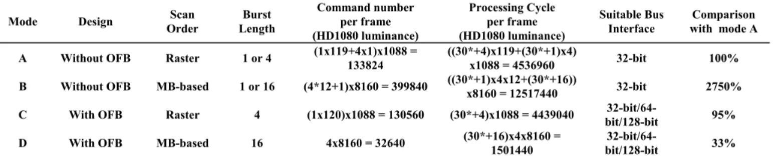
architecture for real-time applications. Table III shows the evaluation of the required memory bandwidth in real cases with the proposed OFB. If we use MB-based scan order without using the OFB architecture, it will increase the number of bus commands since the write out shape is not a complete MB shape. So it will take about 27.5 times of processing cycles than the traditional raster scan. By using the proposed OFB, we can avoid the cross 1K boundary problem and reduce the number of commands (for both raster scan and MB-based scan). By reducing 75% commands required in MB-based scan order, we can also reduce 67% bus latency (assuming bus delay cycle/command = 30) compared to that in the traditional raster scan deblocking filter. Thus, we can achieve high efficiency data access by using the proposed architecture.
Fig. 24. H.264 realtime decoding with the proposed deblocking filter design on a FPGA platform
V. CONCLUSION
A high efficiency data access VLSI architecture for multiple-standard in-loop deblocking filters has been presented. First, we analyze the MBAFF algorithm in the H.264 deblocking filter so that the reference data can be reconfigured as baseline profile reference data for the 1-D filter. Therefore, we can share the same 1-D filter architecture for supporting several different video coding protocols, i.e. H.264, SVC, MVC, VC-1, and AVS. Second, we use the same filter order to support deblocking filtering of both H.264 8x8 blocks and AVS by controlling the BS values. Third, we use a PDM to control MB data for different MB types to support both interlaced frame and MBAFF frame. Two internal buffers are utilized to store the MBAFF reference data for reducing the data access from external memory. This buffer management can be used in the deblocking filtering for other standards such as VC-1 and AVS. Then, we reduce the bus latency by avoiding the cross 1K boundary problem and increase the bus burst length by using MB-based scan order. By using these techniques, we can achieve 67% reduction in processing cycles. After being implemented by using a 90nm CMOS technology, the proposed work reaches a maximum frequency of 370 MHz. This high clock rate enables the proposed work to save power consumption by scaling down supply voltage as long as enough performance capability is achieved.
TABLEIII
HIGH EFFICIENCY MEMORY ACCESS THROUGH THE PROPOSED OFB
Mode Design Order Scan Length Burst
Command number per frame (HD1080 luminance) Processing Cycle per frame (HD1080 luminance) Suitable Bus Interface Comparison with mode A
A Without OFB Raster 1 or 4 (1x119+4x1)x1088 = 133824 ((30*+4)x119+(30*+1)x4) x1088 = 4536960 32-bit 100%
B Without OFB MB-based 1 or 16 (4*12+1)x8160 = 399840 ((30*+1)x4x12+(30*+16)) x8160 = 12517440 32-bit 2750%
C With OFB Raster 4 (1x120)x1088 = 130560 (30*+4)x1088 = 4439040 bit/128-bit 32-bit/64- 95%
D With OFB MB-based 16 4x8160 = 32640 (30*+16)x4x8160 = 1501440 bit/128-bit 32-bit/64- 33%
*: Assuming bus delay cycle per memory access command = 30
TABLEII
HARDWARE COMPARISONS WITH OTHER DESIGNS
Design Support Standard Filter Core Number Synthesis Technology
Processing Cycles per MB (worst case) Gate Count Memory Requirement (Byte) Working Frequency (MHz) Huang [3] H.264 BP 1 0.25μm 614 20.66K 640 100 Sheng [4] H.264 BP 1 0.25μm 446 24K 1000 100 Liu [5] H.264 BP 1 0.18μm 250 19.64K 864+8N 100 Tsai [13] H.264 BP 4 0.13μm 48 20.14K 256* 250 Chung [14] H.264 BP 1 0.18μm 198 19.8K 1616 200 Lee [6] VC-1 1 0.18μm 527 12.4K 1088 180
Sheng [8] AVS JP 1 0.18μm N/A 30K 384 140
Chen [9] AVS JP 1 N/A 168 N/A 388 N/A
Liu [10] H.264 BP MPEG4 1 0.18μm 250 19.64K 864+8N 100 Proposed Design H.264 BP/MP/HP SVC/MVC VC-1 AVS JP 1 90nm 160 38.4K** 50.6K*** 672** 2464*** 370
678 IEEE Transactions on Consumer Electronics, Vol. 58, No. 2, May 2012
REFERENCES
[1] C. A. Chien, H. C. Chang, and J. I. Guo, “A High Throughput In-Loop De-blocking Filter Supporting H.264/AVC BP/MP/HP Video Coding,” Proc.
IEEE APC-CAS, pp.312-315, Dec. 2008.
[2] C. A. Chien, H. C. Chang, and J. I. Guo, “A High Throughput Deblocking Filter Design Supporting Multiple Video Coding Standards,” Proc. IEEE
ISCAS, pp.2377-2380, May 2009.
[3] Y. W. Huang, T. W. Chen, B.Y. Hsieh, T. C. Wang, T. H. Chang, and L. G. Chen, “Architecture design for deblocking filter in H.264/JVT/AVC,” Proc.
IEEE ICME, vol.1,pp. I - 693-6, July 2003.
[4] B. Sheng, W. Gao, and D. Wu, “An Implemented architecture of deblocking filter for H.264/AVC,” Proc. IEEE ICIP, vol.1, pp. 665-668, Oct. 2004. [5] T. M. Liu, W. P. Lee, T. A. Lin, and C. Y. Lee, “A memory-efficient
deblocking filter for H.264/AVC video coding,” Proc. IEEE ISCAS, pp. 2140-2143, May 2005.
[6] Y. L. Lee, and T. Nguyen, “Analysis and Integrated Architecture Design for Overlap Smooth and In-Loop Deblocking Filter in VC-1,” Proc. IEEE ICIP, vol.5, pp. 169-172, 2007.
[7] R. Citro, M. Guerrero, J. B. Lee, and M. Pantoja, “Programmable Deblocking Filter Architecture for a VC-1 Video Decoder,” IEEE Trans.
Circuits Syst. Video Technol., vol. 19, No.8, pp.1227-1233, Aug. 2009.
[8] B. Sheng, W. Gao, and D. Wu, "A Platform-based Architecture of Loop Filter for AVS,“IEEE ICSP, vol. 1, September 2004.
[9] Q. Chen, Q. M. Yi, and M. Shi, “High-Performance Deblocking Filter Design and Implementation for AVS HDTV Applications,” Proc. IEEE
WiCOM, pp. 1-4, 2011.
[10] T. M. Liu, W. P. Lee, and C. Y. Lee, “An in/post-loop deblocking filter with hybrid filtering schedule,” IEEE Trans. Circuits Syst. Video Technol., vol. 17, No.7, pp.937-943, Jul. 2007.
[11] Y. X. Zhao, and A. P. Jiang, “A novel parallel processing architecture for deblocking filter in H.264 using vertical MB filtering order,” Proc. ICSSIC T, pp.2028-2030, Shanghai, 2006.
[12] K.Y. Min and J. W. Chong, “A memory and performance optimized architecture of deblocking filter in H.264/AVC,” Proc. ICMUE, pp.220-225, Seoul Korea, April 2007.
[13] T. H. Tsai, and Y. N. Pan, “High Efficient H.264/AVC Deblocking Filter Architecture for Real-time QFHD,” IEEE Trans. Consumer Electron., vol. 55, no. 4, pp. 2248-2256, Nov. 2009
[14] H. C. Chung, Z.Y. Chen, and P. C. Chang, “Low Power Architecture Design and Hardware Implementations of Deblocking Filter in H.264/AVC,” IEEE
Trans. Consumer Electron., vol. 57, no. 2, pp. 713-719, May 2011
[15] Proposed SMPTE Standard for Television: VC-1 Compressed Video Bit-stream Format and Decoding Process, “SMPTE 421M,” 2005.
BIOGRAPHIES
Cheng-An Chien was born in Taipei, Taiwan, R. O. C., in
1983. He received the B.S. degree and M.S. degree in Department of Computer Science and Information Engineering from National Chung Cheng University, Chia-Yi, Taiwan, in 2006 and 2008, respectively. He is currently working on his Ph.D. degree in Department of Computer Science and Information Engineering at National Chung Cheng University. His research interests include video processing algorithm, 3D display algorithm, VLSI architecture design, and digital IP design.
Guo-An Jian was born in Taichung, Taiwan, in 1980. He
received the B.S. and M.S. degrees in computer science from National Chung-Cheng University, Chia-Yi, Taiwan, in 2003 and 2005, respectively. He is currently a Ph.D. candidate in the Department of Computer Science and Information Engineering, National Chung-Cheng University, Chia-Yi, Taiwan. His research interests include software optimization and parallel computing for video technology.
Hsiu-Cheng Chang was born in Tainan, Taiwan, R.
O. C., in 1981. He received the B.S. and M.S. degrees in Department of Computer Science and Information Engineering from National Chung Cheng University, Chia Yi, Taiwan, in 2003 and 2005 respectively. He is currently working toward the Ph.D. degree at the Graduate Institute of Computer Science and Information Engineering, National Chung Cheng University. His research interests include video processing, VLSI architectures, digital IP design and multimedia SOC design.
Kuan-Hung Chen received the B.S. and the M.S.
degrees from National Cheng Kung University, Tainan, Taiwan, in 1998 and 2000, respectively. Since September 2002, he started to pursue his Ph.D. degree, and received the Ph.D. degree from National Chung Cheng University, Chiayi, Taiwan in March 2006. Then, he became a Post-doctorial Fellow in the System-on-a-Chip (SoC) technology research center and department of electrical engineering, National Chung Cheng University. Since February 2007, he has been with the department of electronic engineering, Feng-Chia University, Taichung, Taiwan, as an Assistant Professor, where he became an Associate Professor in August 2011. He has received a scholarship from National Chip-Implementation-Center (CIC), Taiwan, for his enthusiastic contribution on low-power multimedia silicon intellectual property (SIP) designs in 2005. His research interests include VLSI design for multimedia coding, 3D visual computation, intelligent electronics, and related low-power technology for the above VLSI designs.
Dr. Chen is the recipient of the Annual Paper Award, a.k.a. Professor Wen-Zen Shen Memorial Award, from Taiwan IC Design Society (TICD) in 2006, and won the 2nd-Prize of the National Silicon Intellectual Property (SIP) Design Contest, Taiwan twice in 2004, and 2005, respectively.
Jiun-In Guo received the B.S. and Ph.D. degrees in
electronics engineering from National Chiao Tung University, Hsinchu, Taiwan, in 1989 and 1993, respectively. He is currently a full Professor of the Dept. of Electronics Engineering, National Chiao-Tung University, Hsinchu, Taiwan. He has been the Director of the Dept. of Computer Science, National Chung-Cheng University, Taiwan during 2009-2011 and has been the Research Distinguished Professor of National Chung-Cheng University since 2008. He joined the System-on-Chip (SOC) Research Center in March 2003, to get involved in several Grand Research Projects on low-power, high-performance processor design, and multimedia IP/SOC design. He was the Director of the SOC Research Center, National Chung-Cheng University, from 2005 to 2008. He was an Associate Professor of the Dept. of Computer Science and Information Engineering, National Chung-Cheng University, from 2001 to 2003, and an Associate Professor of the Dept. of Electronics Engineering, National Lien-Ho Institute of Technology, Miaoli, Taiwan, from 1994 to 2001. His research interests include images, multimedia, and digital signal processing, VLSI algorithm/architecture design, digital SIP design, and SOC design. He is the author of over 160 technical papers on the research areas of low-power and low cost algorithm and architecture design for DSP/Multimedia signal processing applications.