Abstract—In this paper, a new current-mode front-end ampli-fier (CMFEA) for neural signal recording systems is proposed. In the proposed CMFEA, a current-mode preamplifier with an active feedback loop operated at very low frequency is designed as the first gain stage to bypass any dc offset current generated by the electrode-tissue interface and to achieve a low high-pass cutoff frequency below 0.5 Hz. No reset signal or ultra-large pseudo resistor is required. The current-mode preamplifier has low dc operation current to enhance low-noise performance and decrease power consumption. A programmable current gain stage is adopted to provide adjustable gain for adaptive signal scaling. A following current-mode filter is designed to adjust the low-pass cutoff frequency for different neural signals. The proposed CMFEA is designed and fabricated in 0.18- CMOS technology and the area of the core circuit is 0.076 . The measured high-pass cutoff frequency is as low as 0.3 Hz and the low-pass cutoff frequency is adjustable from 1 kHz to 10 kHz. The measured maximum current gain is 55.9 dB. The measured input-referred current noise density is 153 , and the power consumption is 13 at 1-V power supply. The fabri-cated CMFEA has been successfully applied to the animal test for recording the seizure ECoG of Long-Evan rats.
Index Terms—Current-mode, front-end, low-noise low power design, neural recording, offset cancellation.
I. INTRODUCTION
I
T is known that the acquisition device for neural signal recording is one of the most important components in a biomedical electronic system. In the acquisition device, the Front-End Amplifier (FEA) is one of the key elements, which senses and amplifies the neural signals such as Electrocorticog-raphy (ECoG), Electrocardiogram (ECG), action potential, local field potential (LFP) etc., through electrode-tissue inter-faces. Since the amplitude of neural signals is very small and the electrodes are easily interfered by external noise sources Manuscript received September 30, 2012; revised January 17, 2013 and March 17, 2013; accepted March 18, 2013. Date of publication April 25, 2013; date of current version May 03, 2013. This work was supported in part by the National Science Council (NSC), R.O.C., under project NSC-101-2220-E-009-017, and by “Aim for the Top University Plan” of the National Chiao Tung University and Ministry of Education, Taiwan. This paper was recommended by Associate Editor P. Georgiou.C.-Y. Wu is with the Department of Electronics Engineering, Institute of Electronics, National Chiao Tung University, Hsinchu 300, Taiwan, and is also with the Biomedical Electronics Translational Research Center, National Chiao Tung University, Hsinchu 300, Taiwan (e-mail: [email protected]).
W.-M. Chen and L.-T. Kuo are with the Department of Electronics Engi-neering, Institute of Electronics, National Chiao Tung University, Hsinchu 300, Taiwan.
Color versions of one or more of the figures in this paper are available online at http://ieeexplore.ieee.org.
Digital Object Identifier 10.1109/TBCAS.2013.2256422
like 60-Hz noise from power lines or other disturbance sources, a low-noise FEA is required. With the increasing number of input electrodes required for clinical and implant applications, a FEA must meet the requirements of low power consumption and small chip area. The required low-pass cutoff frequency for neural signals varies from several hundred Hz to kilo Hz whereas the required high-pass cutoff frequency is below 0.1 Hz. Thus the low-pass cutoff frequency of FEAs should be adjustable. Moreover, the amplitude of the dc input offset voltage caused by the electrode-tissue interface varies with both material and size of electrodes. It must be eliminated to prevent the saturation of FEAs while amplifying neural signals below 0.1 Hz.
To reject the dc offset, the AC coupled techniques are pro-posed in some voltage-mode FEAs. In [1]–[3], MOS-bipolar or MOS pseudo resistors are adopted to realize ultra-large resis-tances which are highly dependent on the voltage across them. This causes large signal distortions and large variations of high-pass filter characteristics. Moreover, a reset signal is required [3] to reset the pseudo resistor and keep the bias condition stable. This makes the circuit design more complicated and the peri-odic reset signal causes the switched-capacitor effect which de-grades the high-pass cutoff frequency. On the other hand, large external capacitors are used to achieve a high-pass cutoff fre-quency below 1 Hz [4], [5]. However, the use of discrete com-ponent increases the size of acquisition devices and limits the use of devices in implantable applications.
Generally, the internal nodes in current-mode circuits have low impedance characteristics and low voltage swings. Thus power supply voltage can be reduced to decrease the power con-sumption. The voltage noise is inversely proportional to dc op-erating current whereas the current noise is proportional to dc operating current. Thus current-mode circuits can achieve low noise under low power consumption.
Several current-mode circuits [6], [7] have been proposed for amplifier applications. In [6], a CMOS front-end amplifier for photo-current acquisition is presented with a feedback loop consisted of a sample-and-hold stage, an error amplifier, and a sinking device to bypass the flowing-out dc current. In [7], a trans impedance amplifier (TIA) consisted of an integrator followed by a differentiator is proposed to amplify the current signals of nanodevices. The dc offset current flows into the low-frequency feedback path and is rejected without affecting the in-band signal. However, the high-pass cutoff frequency (100 Hz–1 kHz) is too high for neural signals. The power dissi-pation is 45 mW which is not suitable for low-power FEAs.
In this paper, a new low-power current-mode front-end am-plifier (CMFEA) for neural signal recording is proposed. In 1932-4545/$31.00 © 2013 IEEE
Fig. 1. Block diagram of the proposed current-mode front-end amplifier (CMFEA).
the proposed CMFEA, the biological signal current flowing in the input electrode-tissue interface as generated by the biopo-tential signal, is sensed and amplified. The proposed CMFEA can retain the advantages of low power consumption and low power supply in current-mode circuits. It also has a good noise rejection capability. As compared to the voltage-mode ampli-fiers, neither ultra-high value pseudo resistors with reset signals nor external large capacitors are required. Moreover, the current preamplifier with the cancellation feedback loop is designed to bypass the dc offset current generated by the electrode-tissue in-terface so that the dc offset current does not affect the amplifier operation.
The proposed CMFEA is designed and fabricated in 0.18-CMOS technology. The measurement results show that the high-pass cutoff frequency of 0.3 Hz can be achieved whereas the low-pass cutoff frequency can be adjusted from 1 kHz to 10 kHz. The measured input-referred current noise density is 153 . The power dissipation is 13 at 1-V power supply. The chip area is 0.576 with 0.076 of the core CMFEA circuit. The animal test on the ECoG signal recording of epileptic Long-Evan rats is demonstrated. These experimental results have verified that the proposed CMFEA is a potential solution for neural signal recording systems.
II. CIRCUITDESIGN
The architecture of the proposed CMFEA is shown in Fig. 1 which consists of a current-mode preamplifier with an active feedback loop, a programmable current gain stage, and a tunable current-mode filter. The first stage is the current-mode pream-plifier designed to amplify the band current signals. The in-corporated active feedback loop is operated at a very low fre-quency to bypass the dc offset current generated from the elec-trode-tissue interface. The second stage is the programmable current amplifier which provides further amplification and ad-justable signal gain for different neural signals. The third stage is a tunable current-mode filter. Its low-pass cutoff frequency is adjustable from 1 kHz to 10 kHz. A TIA is designed to convert the output current signal to voltage for measurement.
A. Current-Mode Preamplifier
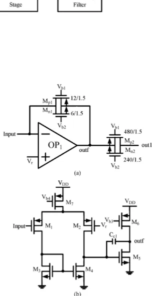
Since the noise of the first stage is the dominate noise source, a current-mode preamplifier with low dc current is used as the first stage to suppress the noise contributed by this stage [8]. The structure of the current-mode preamplifier with low dc current is shown in Fig. 2(a) [8]. The operational amplifier is de-signed with a two-stage topology as shown in Fig. 2(b) where the aspect ratio of is identical to that of . In
Fig. 2. (a) Structure of current-mode preamplifier. (b) Circuit schematic of .
Fig. 2(a), the dc voltages of the input node and the node outf are
set to via the negative feedback loop
of . The voltage of out1 is also set to via the negative feedback loop in the next stage. As a result, the dc drain-source voltages of , , , and are kept at 0 V. With and , all devices are operated at a very low dc current in the linear subthreshold region as resistors. Since the channel lengths of and are the same, the resistance ratio of to is equal to the channel width ratio of to which is designed to be 40. With a small-signal input current flowing on , the small-signal voltage across is the same as that of . Thus the current on is equal to 40 and a current gain of 40 can be obtained. The current-mode preamplifier in Fig. 2(a) has low input impedance and distortion.
In the circuit of Fig. 2(b), form an ampli-fier with the current-mirror load . Using PMOS as input devices can reduce the flicker noise. The is designed
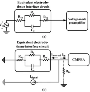
Fig. 3. (a) The equivalent electrode-tissue interface circuit with the voltage-mode preamplifier. (b) Norton equivalent circuit of the electrode-tissue interface circuit with the CMFEA.
to achieve low offset voltage with suitable gain. Therefore, the sizes of which are the main contributions of offset are enlarged to decrease the offset caused by device mismatch.
The equivalent electrode-tissue interface circuit with the voltage-mode preamplifier is shown as Fig. 3(a). Its Norton equivalent circuit with the CMFEA is shown as Fig. 3(b). In Fig. 3, is the spreading resistance between electrolyte and tissue, and are the resistance and capacitance of the electrode-tissue interface, respectively, is the resistance of the electrode, is the neural potential signal, is the input impedance of the CMFEA, is the current signal injecting into the current-mode preamplifier, and is the internal signal current flowing through the interface circuit in Fig. 3(b). Unlike voltage-mode preamplifiers whose input impedance should be designed as high as possible, the input impedance of current-mode preamplifier should be designed as low as pos-sible to sense the input current signal. Thus the current signal generated by the neural signal on the input electrode-tissue interface can flow into the current-mode preamplifier with less degradation as can be seen from Fig. 3(b).
Note that the recorded current signal is generated by the neural potential signal on the input electrode-tissue interface and dependent on interface impedance. It can be used directly to extract physiological features like epileptic seizure occurrence. The recorded current signal can also be converted into the corresponding neural potential signal by using an analog TIA with the transimpedance equivalent to the electrode interface impedance.
Since the measured equivalent impedance of electrode is about 1 at dc and 100 at 10 kHz, the input resistance of the current-mode preamplifier is designed to be 4.6 which is determined by , , and the gain of as
(1)
voltage signal in the range of mV. In the proposed current-mode preamplifier, the input signal current is also in the range of nA when the kHz voltage signal in the range of mV.
The input referred current noise of the current-mode preamplifier can be expressed as [8]
(2) where is the Boltzmann constant, is the absolute tempera-ture, is the transconductance of MOS device, is the signal frequency, is the input capacitance of , is the input referred voltage noise of , and is the bandwidth of the preamplifier.
The first term in (2) is mainly contributed by and proportional to the transconductance. Thus, low dc currents in the devices result in a low noise performance. Since are operated at low dc currents and their noise con-tribution to the equivalent input noise is divided by the gain of 40, the noise influence of is negligible.
In the second term in (2), is contributed by the flicker
noise and the thermal noise of the
devices in , which can be expressed as
(3) (4) (5) (6) (7) (8) where , , , , and are the output resistance, width, length, gate capacitance density, and the mobility of the MOS device, respectively, and is the process-dependent constant of flicker noise. From (5), the thermal noise can be reduced by increasing . Thus, the bias current in the first stage of is increased to increase and reduce the thermal noise con-tributed to the preamplifier. Since the flicker noise is inversely
Fig. 4. (a) Structure of the feedback loop. (b) Circuit schematic of .
proportional to in (8), is designed with a long device channel length to reduce the flicker noise.
To avoid the effect of long length in limiting the signal swings, is designed with a large device width . Since the input noise is independent of , large does not increase the noise. is also designed to be larger to reduce both thermal and flicker noises.
B. Active Feedback Loop
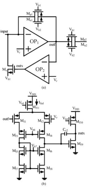
Fig. 4(a) shows the active feedback loop with the current-mode preamplifier. The loop consists of the transistor and the operational amplifier . The purpose of the feedback loop is to take the flowing-in dc offset current that could exist in the electrode-tissue interface. In the experimental chip design, only one direction of dc offset current is considered. The loop for the flowing-out one can be similarly designed.
In the proposed current-mode preamplifier, the input dc offset current is determined by the resistance of the electrode-tissue in-terface and the input resistance of the preamplifier as well as the dc offset voltage across of the electrode-tissue interface and the input dc offset voltage of the preamplifier. Thus both dc offset
Fig. 5. Circuit structure of the programmable current gain stage.
voltages should be kept as small as possible to minimize the input dc offset current. With appropriate op amp design and an-imal test setup, the total input dc offset voltage can be minimized to tens of uV. The total dc resistance of the preamplifier input loop is in the mega ohm order. Thus, the input dc offset current can be minimized to the pA range to avoid the damage to the tissue or electrodes.
When the input dc offset current flows into the preamplifier, the output voltage of is changed to drive which gen-erates a similar dc current to bypass the input dc offset current. The amount of the bypass current can be derived as
(9) where is the resistance of and , is the transconductance of , is the gain of , and is the input dc offset current. The feedback loop is designed to bypass 99% of input dc offset current.
The amplifier used in the feedback loop is shown in Fig. 4(b) where the telescopic architecture with a common-source second stage is used. High output resistance of telescopic architecture with the miller compensation capacitor can achieve a very low 3-dB cutoff frequency of 0.24 mHz. The high-pass cutoff frequency of the overall preamplifier in Fig. 4(a) can be derived as
(10) where is the low 3-dB cutoff frequency of , is the dc bias current of input stage in , is the weak inversion slope factor, and is the thermal voltage. As can be seen from (10), varies with which depends on directly. The variation can be compensated by adjusting to keep the high-pass cutoff frequency fixed for different input dc offset currents.
The output noise of the in Fig. 4(a) contributes the noise current to the input node through . But since is designed to be at zero operating current, the generated noise current is very small. Thus, the noise contribution of and can be neglected.
Fig. 6. Schematic of the first-order log-domain current-mode filter.
C. Programmable Current Gain Stage
Since the output dc voltage of out1 in the proposed current preamplifier of Fig. 2(a) has to be clamped to by the next stage, a programmable current gain stage incorporated with a negative feedback loop is proposed as the second stage. The structure of the programmable current gain stage is shown in Fig. 5. Since the noise of the second stage is not the dominate source, the multi-stage current mirror is designed as the pro-grammable current gain stage. In Fig. 5, has a two-stage structure as shown in Fig. 2(b). It is used not only to clamp the voltage of out1, but also to reduce the input impedance of the stage. This also reduces the variations of input impedance with different input signal currents so that the signal distortion can be minimized and the linearity can be improved. The input impedance of the programmable current gain stage can be de-rived as
(11) (12) where is the gain of and is the transconduc-tance of . is operated in the subthreshold region, thus the input impedance can be expressed as (12) where is the dc bias current in , and is the input current signal flowing in to the programmable current gain stage. It can be seen from (12) that the input impedance is reduced by a factor of . Thus the current injection efficiency can be increased.
The current amplification ratio is determined by the MOS size ratio. When turns on, the parallel-connection number of and is increased and the current gain is reduced. On the other hand, when turns off, the transistors of and are turned off and the current gain is increased. With digital control signals on the switches and , the number of parallel-connection transistors is selected to adjust the current gain. The current gain can be adjusted from 12 dB to 24 dB in four steps.
D. Tunable Current-Mode Filter
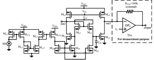
A first-order log-domain current-mode filter is used as shown in Fig. 6 [9] where the transistors , , , and
are operated in the weak inversion region. The low-pass cutoff frequency is described as
(13) where is the current of and , and is the ca-pacitor used in the current-mode filter. From (13), the low-pass cutoff frequency of the current-mode filter can be designed at a very low frequency by applying a low without the use of large capacitance. By adjusting , the low-pass cutoff fre-quency of the CMFEA can be tuned from 1 kHz to 10 kHz.
In Fig. 6, the TIA with a 100 k external resistor is used to con-vert the output current signal to voltage signal for measurement purpose, since there is no measurement equipment available to measure the current signal directly. In the integration of the pro-posed CMFEA with ADC, the TIA with the external resistor is not required.
III. EXPERIMENTRESULTS
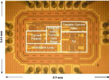
The proposed CMFEA has been designed and fabricated by TSMC 0.18- CMOS technology. The chip photograph of the fabricated circuit is shown in Fig. 7. The total chip area is 0.576 including the ESD pad. The chip areas of the core circuit are 0.076 and 0.135 without and with the TIA, respectively.
In the measurement setup for functionality test, the input voltage signal is fed into the discrete circuit which is the same as the equivalent electrode-tissue interface circuit as shown in Fig. 3(a). Thus, the voltage signal can be converted into current signal through the discrete circuit and fed into the CMFEA.
The measured frequency response is shown in Fig. 8 where low-pass and high-pass cutoff frequencies are both tunable. The low-pass cutoff frequency is located in the range of 1 kHz to 10 kHz with to 1 nA as shown in Fig. 8(a) and Fig. 8(b), respectively. The high-pass cutoff frequency can be as low as 0.3 Hz when the input dc current is 5 nA. The maximum gain is 55.9 dB. The maximum input dc offset current which can be bypassed by the active feedback loop is 15 nA with the high-pass cutoff frequency remains below 1 Hz.
The measurement result of the THD is shown in Fig. 9 where the input signal has the maximum operation frequency (10 kHz)
Fig. 7. Chip photograph of the fabricated CMFEA.
Fig. 8. The measured frequency response with (a) 1 kHz low-pass cutoff fre-quency and (b) 10 kHz low-pass cutoff frefre-quency.
and 20 nAp-p peak-to-peak amplitude. It can be seen that under the maximum input signal 20 nAp-p which is much higher than the normal neural signal, the THD is 1.03%. Thus the proposed CMFEA has a low THD. The measured output current noise from 1 Hz to 10 kHz is shown in Fig. 10. The measured input-re-ferred current noise is 15.3 . By using the maximum input current of 7.07 nArms, the SNR or maximum dynamic range of the CMFEA can be calculated as
.
The fabricated CMFEA chip is applied to the measurement of ECoG signals of Long-Evan rats. Fig. 11 shows the measure-ment setup of the animal test where the recording electrode is
Fig. 9. The measured frequency spectrum of output current when at 10 kHz.
Fig. 10. The measured output current noise from 1 Hz to 10 kHz.
connected to the CMFEA with wire. The ECoG signal is sensed and amplified by the CMFEA and the amplified signal is mea-sured by the oscilloscope.
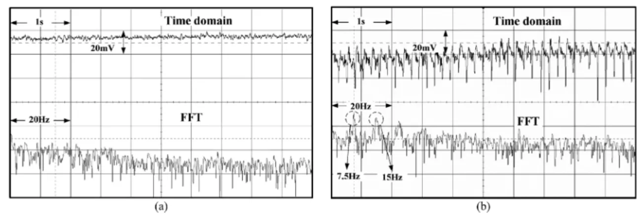
Figs. 12(a) and (b) show the ECoG measurement results of the animal test in both time and frequency domains with the gain of CMFEA set to 55.9 dB. Fig. 12(a) shows the measured normal ECoG signal. As can been seen from Fig. 12(a) that the amplitude variations of the transient waveform are small and no specific component is shown on the spectrum. Fig. 12(b) shows the measured ECoG signal when the rat has epileptic seizures. In Fig. 12(b), the corresponding input current is around 0.3 nA. As can be seen from the measured spectrum, the main frequency components are around 7.5 Hz and 15 Hz which are identical with the measurement results of voltage-mode amplifiers.
The experimental results are summarized in Table I with the comparisons to other reported voltage-mode FEAs. With the same bandwidth of 7 10 kHz, the power consumption of the proposed current-mode front-end amplifier is less than other voltage-mode FEAs. The formula of the noise efficiency factor (NEF) is
(14) where is the input-referred rms noise voltage, is the total supply current, and is the amplifier bandwidth. To calculate the NEF of the proposed CMFEA, the input noise current density referred to the input node of the electrode is con-verted to the input noise voltage density by multiplying the mea-sured impedance of the electrode with ,
Fig. 11. The measurement setup of the animal test.
Fig. 12. The measured ECoG signals of the rat when in the (a) normal state and (b) epileptic seizure state.
TABLE I
PERFORMANCESUMMARY ANDCOMPARISON OFFEAS
a. Area per channel. b. w/o TIA. c. w/TIA. d. Current gain. e. Voltage gain. f. Bandwidth of 200 Hz. g. Bandwidth of 200–6.2 kHz. h. Only the first stage. i. Referred to the input node of the electrode. j. Referred to the input node of the CMFEA.
, and as shown in Fig. 3(b).
The calculated NEF of the CMFEA is 5.45. For the NEF
re-ferred to the input node of the CMFEA which is adopted in voltage-mode FEAs, the input impedance value of 4.6 and
NEF is 0.10. Unlike voltage-mode FEAs, the CMFEA has low input impedance which leads to low input noise voltage. Thus the calculated NEF of the CMFEA can be as low as 0.10.
IV. CONCLUSION
In this paper, a new CMOS current-mode front-end amplifier (CMFEA) for neural signal recording is proposed. In the pro-posed CMFEA, both bandwidth and current gain are all tunable for different neural signals. Through an active feedback loop incorporated with the first-stage current-mode preamplifier, the high-pass cutoff frequency can achieve 0.3 Hz and the dc offset current caused by electrode-tissue interface can be bypassed. No reset signal or ultra-high value pseudo resistor is needed in the CMFEA. The measured input referred current noise density is 153 with the bandwidth up to 10 kHz. The power dis-sipation is 13 at 1-V power supply. The proposed CMFEA is also applied to the animal test successfully to measure the epileptic ECoG of rats. The experimental results have demon-strated that the CMFEA is a promising solution for designing low-noise and low-power neural recording amplifiers.
ACKNOWLEDGMENT
The authors would like to thank National Chip Implementa-tion Center (CIC) for technical support and chip fabricaImplementa-tion.
REFERENCES
[1] R. R. Harrison and C. Charles, “A low-power low-noise CMOS am-plifier for neural recording applications,” IEEE J. Solid-State Circuits, vol. 38, no. 6, pp. 958–965, Jun. 2003.
[2] M. Yin and M. Ghovanloo, “A low-noise preamplifier with adjustable gain and bandwidth for biopotential recording applications,” in Proc. IEEE Int. Symp. Circuits Syst., May 2007, pp. 321–324.
[3] R. R. Harrison, “A versatile integrated circuit for the acquisition of biopotentials,” in Proc. IEEE Custom Integrated Circuits Conf., Sep. 2007, pp. 115–122.
[4] R. F. Yazicioglu, P. Merken, R. Puers, and C. Van Hoof, “A 60 60 readout front-end for portable biopotential acquisition systems,” IEEE J. Solid-State Circuits, vol. 42, no. 5, pp. 1100–1110, May 2007.
[5] S.-T. Kao, H. Lu, and C. Su, “A 1.5 V 7.5 uW programmable gain amplifier for multiple biomedical signal acquisition,” in Proc. IEEE Biomedical Circuits and Syst. Conf., Nov. 2009, pp. 73–76. [6] A. K. Y. Wong, K.-P. Pun, Y.-T. Zhang, and K.-N. Leung, “A
low-power CMOS front-end for photoplethysmographic signal acquisition with robust DC photocurrent rejection,” IEEE Trans. Biomed. Circuits Syst., vol. 2, no. 4, pp. 280–288, Dec. 2008.
[7] G. Ferrari, F. Gozzini, A. Molari, and M. Sampietro, “Transimpedance amplifier for high sensitivity current measurements on nanodevices,” IEEE J. Solid-State Circuits, vol. 44, no. 5, pp. 1609–1616, May 2009. [8] G. Ferrari, M. Farina, F. Guagliardo, M. Carminati, and M. Sampi-etro, “Ultra-low-noise CMOS current preamplifier from DC to 1 MHz,” Electron. Lett., vol. 45, no. 25, pp. 1278–1280, Dec. 3, 2009. [9] J. Mulder, W. A. Serdijn, A. C. Van der Woerd, and A. H. M. van
Roermund, Dynamic Translinear and Log-Domain Circuits: Analysis and Synthesis. Boston, MA, USA: Kluwer, 1998.
[10] N. Verma, A. Shoeb, J. Bohorquez, J. Dawson, J. Guttag, and A. P. Chandrakasan, “A micro-power EEG acquisition SoC with integrated feature extraction processor for a chronic seizure detection system,” IEEE J. Solid-State Circuits, vol. 45, no. 4, pp. 804–816, Apr. 2010.
[11] M. Azin, D. J. Guggenmos, S. Barbay, R. J. Nudo, and P. Mohseni, “A battery-powered activity-dependent intracortical mcrostimulation IC for brain-machine-brain interface,” IEEE J. Solid-State Circuits, vol. 46, no. 4, pp. 731–745, Apr. 2011.
[12] C. M. Lopez, D. Prodanov, D. Braeken, I. Gligorijevic, W. Eberle, C. Bartic, R. Puers, and G. Gielen, “A multichannel integrated circuit for electrical recording of neural activity, with independent channel pro-grammability,” IEEE Trans. Biomed. Circuits Syst., vol. 6, no. 2, pp. 101–110, Apr. 2012.
Chung-Yu Wu (S’76–M’76–SM’96–F’98) was
born in 1950. He received the M.S. and Ph.D. degrees in electronics engineering from National Chiao Tung University, Hsinchu, Taiwan, in 1976 and 1980, respectively.
Since 1980, he has been a Consultant to high-tech industry and research organizations and has built strong research collaborations with high-tech in-dustries. From 1980 to 1983, he was an Associate Professor with National Chiao Tung University. From 1984 to 1986, he was a Visiting Associate Pro-fessor with the Department of Electrical Engineering, Portland State University, Portland, OR, USA. Since 1987, he has been a Professor with National Chiao Tung University. From 1991 to 1995, he served as the Director of the Division of Engineering and Applied Science, National Science Council, Taiwan. From 1996 to 1998, he was bestowed as the Centennial Honorary Chair Professor of National Chiao Tung University. From 2007 to 2011, he served as the President of National Chiao Tung University. He is currently a Chair Professor of National Chiao Tung University and the Director General of the National Program on Nano Technology, Taiwan. He has authored or coauthored more than 300 technical papers in international journals and conferences. He holds 30 patents, including 17 U.S. patents. His research interests are biomedical electronic devices and systems, intelligent bio-inspired vision sensor systems, nanoeletronic circuits and systems for RF/microwave communication.
Dr. Wu is a member of Eta Kappa Nu and Phi Tau Phi. He was a recipient of the 1998 IEEE Fellow Award and a 2000 Third Millennium Medal. He was also the recipient of numerous research awards presented by the Ministry of Education, National Science Council (NSC), and professional foundations in Taiwan (1999–2003).
Wei-Ming Chen (S’12) was born in Hsinchu,
Taiwan, in 1979. He received the B.S. degree in electrophysics and the M.S. degree in electronics engineering from National Chiao Tung University, Hsinchu, Taiwan, in 2003 and 2005, respectively.
Currently, he is working toward the Ph.D. degree at the Institute of Electronics, National Chiao Tung University. His major research interests are biomed-ical electronics and analog integrated circuits design.
Liang-Ting Kuo was born in Tainan, Taiwan, in
1987. He received the B.S. and M.S. degrees in electronics engineering from National Chiao Tung University, Hsinchu, Taiwan, in 2009 and 2011, respectively.
Recently, he worked at MediaTek, Hsinchu, Taiwan, on analog integrated circuit design.