DESIGN
OF
HIGH-VOLTAGE-TOLERANT POWER-RAIL
ESD CLAMP CIRCUIT
IN
LOW-VOLTAGE
CMOS
PROCESSES
Ming-Dou
Kerl,
Chang-TzuWang'
2,Tien-HaoTang2,and Kuan-ChengSu2 'Nanoelectronics andGigascaleSystemsLaboratoryInstitute of Electronics,National Chiao-Tung University, Hsinchu, Taiwan
2ESDEngineeringDepartment, Reliability Technology & Assurance Division United Microelectronics Corporation, Hsinchu,Taiwan
ABSTRACT
A new high-voltage-tolerant power-rail electrostatic discharge (ESD) clamp circuit with a special ESD detection circuit realized with only IxVDD devices for 3xVDD-tolerant mixed-voltage I/0
interfaces is proposed. The proposed power-rail ESD clamp circuit with excellent ESD protection effectiveness has been verified in a 0.13-ptm CMOS process withonly 1.2-V devices.
INTRODUCTION
With the scaled-down device dimension in advanced CMOS
technology,the power supply voltageis also scaled down to reduce the powerconsumption and to meet the gate-oxidereliability. With consideration of whole systemintegration,theI/0buffers must drive orreceive high-voltage signals to communicate with other ICs in a microelectronic system. Thus, the I/0 buffers should be designed
with high-voltage tolerance to prevent overstress voltage on the thinner gate oxide ofI/0devices [1]. To achieve agoodwhole-chip
ESDprotection scheme for the mixed-voltage I/0 applications, it is required to design the power-rail ESD clamp circuit withonly
low-voltage devices but that can sustain the highpower-supply voltage
without suffering gate-oxide reliability [2]-[4]. The mixed-voltage I/0 buffer to receive 3xVDD input signals by using only IxVDD
low-voltagedevices without suffering gate-oxidereliabilityhas been
reported [5]. Nevertheless, the ESD protection design for such a 3xVDD-tolerant mixed-voltage
I/0
buffer was not considered.Therefore, how to design an effective ESD protection circuit with
only low-voltage devices without suffering gate-oxidereliability for
mixed-voltageI/0buffer with 3xVDDinputtolerance is asignificant challenge.
In this work, a new high-voltage-tolerant ESD clamp circuit realized withonly 1.2-Vlow-voltage devices formixed-voltage I/0
interfaces with 3xVDD input tolerance is proposed. This new
proposed ESDprotection design has no gate-oxide reliability issue under normal circuitoperatingcondition.
Besides,
thisdesignhas an efficient ESD detection circuit totrigger onthe ESD clamp deviceduringESD stress event, sothat theturn-on
efficiency
of ESD clampdevice can besubstantially improved. TheproposedESDprotection design has been successfully verified in a 0.13-ptm CMOS process withonly 1.2-Vdevices.
3
XVDD-TOLERANT
POWER-RAIL
ESD CLAMP
CIRCUIT
WITH
ONLY
1
xVDD DEVICES
The novel 3xVDD-tolerantpower-rail ESDclamp circuit, which contains ESD clampdevice and ESD detection circuit,is shown in
Fig. 1, where the ESD clamp device is realized by a
substrate-triggered SCRwith two diodes in series. The newproposed power-rail ESD clamp circuit is realized with only 1.2-V low-voltage
devicestooperate at3.3-V power supply (3xVDD)without the risk ofgate-oxide reliability.
1-4244-0919-5/07/$2500
©2007
IEEEW.j
594
ESD Detection Circuit ESDClamp Device FIGURE1. THEPROPOSED3xVDD-TOLERANT ESDCLAMP CIRCUIT
REALIZEDWITH ONLY1xVDDDEVICES.
To avoid the damage ofmixed-voltage I/0 buffers before ESD
clamp device is turned on, a turn-on-efficient ESD detection circuit realized with I xVDD devices to sustain 3xVDD signals is essential in such 1.2/3.3-V mixed-voltage I/0 interfaces. The proposedESD detection circuit that can beoperatedunder 3.3-V voltagebias with
only 1.2-Vlowvoltagedevices is shown inFig. 1.Duringthe normal circuitoperating condition with 3xVDD line of 3.3V andgrounded VSS, thevoltage levels at node a and node e in the ESD detection circuit are biased at 2.2V and l.lV, respectively. The gate voltage (node k)of Mp5 will be biased at 0.6V due to thebodyeffect ofMd6,
sothatMp5is turned on and the node d is biased at 1. 1V.Therefore,
Mp3 isturnedoff and there is no triggercurrentgeneratedfrom the ESDdetection circuit into the ESDclampdevice. In thissituation,all 1.2-Vdevices are free fromgate-oxide reliabilityissue under normal circuitoperatingcondition with 3xVDD line of 3.3V.
When ESD voltage is conducted to the 3xVDD line with VSS
relatively grounded, the RCdelayof resistorRI andcapacitorMcl inthe ESD detection circuitkeepnode b at arelativelylowvoltage
level for alongtime. MI and Mp 1 can beturnedonand therefore the
voltage levelsatnodecand nodevriserapidly. The voltage levelsat
node a and node e are initially floatingwith avoltagelevel of OV, sothat M2 andMp2canbeturnedon, and thevoltagelevelsatnode
rand node d also rise as thevoltagelevels at node v and node c. The RC delay of the turn-on resistance of Mp5 and the parasitic capacitance of Mnl keepthe node einalowvoltagelevelto ensure
thatMp3is in the turned-onstateduringESDstress event.Moreover,
the gatevoltageof M5 ishigherthan itssourcevoltagesothat M5 is turnedon tokeepthevoltagelevelatnodeuinalowvoltagelevelas
that at nodee. Therefore, the gate-to-drain voltage of M6 is nearly zero to keepthevoltage level atnode a around thevoltage level at
node eplusathresholdvoltageofM6,when thevoltagelevel at node
a is onethreshold voltage higher than the voltage level at node u. Furthermore,the gatevoltage (node r)ofMp4is ashighasits source
IEEE07CH37867 45th Annual international Reliability Physics
Symposiumr
Phoenix 2007voltage (node c), so that Mp4 is in off state to ensure that the voltage level at node a can be kept in a low voltage level compared with node c. Therefore, the substrate driver of Mpl, Mp2, and Mp3, whose gates are at relatively low voltage levels, can be quickly turned onby ESD energy to generatethe substrate-triggered current into the trigger node (node f) of the SCR. Fig. 2 shows the Hspice-simulated voltages of the ESD detection circuit under ESD stress event. A0-to-6VESD-likepulsewith a rise time of lOns is applied tothe 3xVDD line to simulate the ESD transient voltage. From the simulation results, such low voltage levels at node a, node b, and node e guarantee that Mpl, Mp2, and Mp3 can be turned on during ESD stress event. Therefore, the substrate-triggered current can be
generated by the substrate driver into the trigger node of SCR to
triggeronthe ESDclampdevice to discharge ESD current from the 3xVDDlinetoVSS. -0---nodea 6 L node b+ nodec noded nodee nodef -4-noder W-node u
2
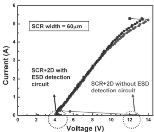
4-u-- 3xVDDline >2 SCRwidth=GOim 4 3 -SCR+2D with ,{ : 2 ESDdetectioncircuit
SCR+2Dwithout ESD| .|t ~~~~detection cir!cuit
0 2 4 *:6 8 10 12 14
"----"Voltage
(V)FIGURE3. THE MEASURED TLP I-V CHARACTERISTICS OFTHEESD CLAMP DEVICE WITH ORWITHOUTESD DETECTION CIRCUIT UNDER
POSITIVE3 xVDD-to-VSS ESD stress.
TABLE1. ESD ROBUSTNESS OFTHEPROPOSEDESD PROTECTION
CIRCUIT WITHVARIOUSSCRWIDTHS
ESDclampdevice HBM ESD MM ESD TLP-measured
(SCR)width(ptm) Level Level It2
30 4kV 260V 2.56A
45 6.2kV 380V 3.82A
60 >8kV 440V 5.31A
Time (ns)
FIGURE 2. HSPICE-SIMULATED VOLTAGES ON NODES OFTHEESD
DETECTION CIRCUIT UNDERO-To-6VESD-LIKETRANSITION WITH A RISE TIME OFIONSON THE3 xVDD LINE.
EXPERIMENTAL
RESULTS
The proposed ESD protection circuit has been fabricated in a
0.13-ptmCMOS processwithonly 1.2-Vdevices. Toinvestigatethe ESDclampdevice behavior with ESD detection circuit during ESD
stress event, transmission line pulse (TLP) generatorwith a pulse
width of 1OOns and a rise time of IOns is used to measured the second breakdown current (It2) of the ESD protection circuit. The TLP-measured I-V characteristics of the ESDclamp device with or without ESD detection circuit under positive ESD stress from
3xVDDlinetoVSSareshown inFig. 3,where the width of SCR in ESDclamp device is 60ptm. From the measured results, thetrigger voltageof ESDclampdevice without ESD detection circuit is 12.7V, whereas thetrigger voltage of ESD clampdevice canbe reducedto only 4.6V by ESD detection circuit without involving the junction
avalanche breakdown. Therefore, the trigger voltage of ESD clamp
devicecanbe significantly reducedby theproposed ESD detection circuitto ensureeffective ESDprotection.
The human-body-model (HBM) ESD levels and machine-model
(MM) ESD levels of the proposed ESD protection circuit with various widths of SCR-based ESDclampdevicesarelisted in TableI.
The HBM ESD levels of ESDprotectioncircuit under SCR widths of
30ptm, 45ptm, and 60ptm are 4kV, 6.2kV, and larger than 8kV, respectively. Besides,the MM ESD levels of ESDprotection circuit under SCR widths of30ptm, 45ptm, and60ptmare 260V, 380V, and
440V, respectively. The corresponding second breakdown current
(It2)measuredbyTLPis also listed in TableI.
CONCLUSION
A new high-voltage-tolerant power-rail ESD clamp circuit with ESD detection circuit realized with only 1.2-V low voltage devices for 3 xVDD-tolerant mixed-voltage I/0 interfaces has been
successfully verified in a 0.13-ptm CMOS process. The ESD detection circuitcansignificantlyreduce thetrigger voltageof ESD
clampdevice. Theproposed power-railESDclampcircuit withhigh
ESD robustness and no gate-oxide reliability issue is an excellent ESD protection solution for the mixed-voltage I/0 interfaces with
high-voltage input/output signals.
REFERENCES
[1] M.-D. Ker, S.-L. Chen,and C.-S.Tsai, "Overview and design of mixed-voltage I/0 buffers with low-voltage thin-oxide CMOS transistors," IEEE Trans. Circuits Syst. I: Regular
Papers,vol. 53,no.9, pp. 1934-1945, Sep. 2006.
[2] M.-D. Ker and K.-H. Lin, "Overview on electrostatic
discharge protection designsformixed-voltage I/0interfaces:
design concept and circuit implementations," IEEE Trans. CircuitsSyst. I:RegularPapers, vol. 53,no. 2,pp. 235-246,
Feb. 2006.
[3] T. Maloney and W. Kan, "Stacked PMOS clamps for high-voltage power supply protection," in Proc. EOSIESD Symp.,
1999,pp.70-77.
[4] W. R. Anderson and D. B. Krakauer, "ESD protection for
mixed-voltage I/0 using NMOS transistors stacked in a
cascode configuration," in Proc. EOSIESD Symp., 1998, pp. 54-62.
[5] M.-D. Ker and S.-L. Chen, "Mixed-voltage I/0 buffer with
dynamic gate-bias circuitto achieve 3xVDD input tolerance
by using