國 立 交 通 大 學
電 機 與 控 制 工 程 學 系
碩 士 論 文
用在移動式機械臂之嵌入式影像處理平台
An Embedded Image Processing Platform for a
Mobile Manipulator
研 究 生:
沈 栢 瀚
指 導 教 授:宋 開 泰 博士
用在移動式機械臂之嵌入式影像處理平台
An Embedded Image Processing Platform for a Mobile
Manipulator
研 究 生:沈柏瀚 Student: Andrian, Henrry
指導教授:宋開泰 博士 Advisor: Dr. Kai-Tai Song
國立交通大學
電機與控制工程學系
碩士論文
A Thesis
Submitted to Department of Electrical and Control Engineering College of Electrical Engineering and Computer Science
National Chiao-Tung University in Partial Fulfillment of the Requirements
for the Degree of Master in
Electrical and Control Engineering July 2004
Hsinchu, Taiwan, Republic of China
用在移動式機械臂之嵌入式影像處理平台
研究生:沈 栢 瀚
指導教授:宋 開 泰 博士 國立交通大學電機與控制工程學系摘 要
本論文的目的在於發展硬體及軟體以實現移動式機械臂的控制系統。
此控制系統採用的是影像資訊之迴授。在硬體實現方面包括一 CMOS 影
像擷取系統以及使用德州儀器 C6416 主處理器之數位信號處理發展
板。使用所建構之嵌入式平台之好處在於可以相對低的價格來提供高
效能之影像處理。在軟體實現方面本文提出了透過基於行為模式的方
式去設計一視覺伺服系統,以解決移動式機械臂的控制問題
。An Embedded Image Processing Platform for a Mobile
Manipulator
Student: Andrian, Henrry Advisor: Dr. Kai-Tai Song
Department of Electrical and Control Engineering National Chiao-Tung University
Abstract
This thesis aims to construct a hardware and software implementation that provides a control scheme for a mobile manipulator. The control scheme uses visual information as feedback. The hardware implementation consists of a CMOS image board and a TI DSP DSK board which uses C6416 as the main processor. The merits of using these two boards are the construction of a low cost embedded platform with high performance. Meanwhile the software implementation proposed a visual servoing using a behavior-based approach to solving the control scheme of the mobile manipulator problem.
Acknowledgments
First and certainly foremost, I wish to acknowledge my advisor, Dr. Kai-Tai Song, for his continuous encouragement, insight, patient guidance and invaluable contribution throughout this study. It was his hard work that has ensured that I was always supported both financially and with the equipment my research required.
I would like to thank Dr. Kuu-Young Yang, Dr. Yu-Lun Huang and Dr. Kun-Wei Lin, for their comments and suggestions for the editing of my thesis.
I would like to thank my uncle Ir. Muis Moksin with his family for giving and supporting financial aid for me to study at National Chiao Tung University (NCTU).
I would like to thank my family, for providing me with the opportunity to undertake my studies at National Chiao Tung University (NCTU). They have provided me with endless support and opportunity to reach new heights.
Lastly, I thank my colleagues in ISCI lab, Chia-How Lin, Chih-Chieh, Chih-How and Yao-Qing for sharing experiences and knowledge during the time of study. I thank my senior Ph.D student Chi-Yi for his helping and guidance during the time of study.
CONTENTS
ABSTRACT(CHINESE)...I ABSTRACT(ENGLISH) ... II ACKNOWLEDGE ... III CONTENTS ...IV LIST OF TABLES ...VI LIST OF FIGURES ... VII
1 . INTRODUCTION ... 1
1.1. Motivation ... 1
1.2. Background and Related Work ... 2
1.2.1. Behavior-based controller... 3
1.2.2. Visual servoing controller... 4
1.2.2.1. Position-based visual servo (PBVS) control ... 5
1.2.2.2. Image-based visual servo (IBVS) control ... 6
1.2.2.3. Camera configuration ... 7
1.3. Problem Statements ... 9
1.4. Organization of the thesis ... 10
2 . EMBEDDED IMAGE PROCESSING PLATFORM... 11
2.1. System Overview... 11
2.1.1. Stand-alone ... 12
2.1.2. Communicate directly with other module ... 12
2.2. CMOS sensor... 15
2.3. DSK6416 daughter board ... 20
2.3.1. Frame buffer (AL422B)... 21
2.3.2. 7 ports GPIO of DSK6416 for emulating 4 COM ports RS232 interface 25 2.4. FPGA (Altera UP2) ... 31
2.4.1. I2C module ... 32
2.4.2. Clock divider module ... 34
2.4.3. Buffer_controller module ... 34
2.4.4. Implementation of the Buffer_controller... 36
2.4.4.1.Acquired image for 15 fps ... 36
2.4.4.2.Acquired image for 30 fps ... 39
2.5. DSK6416 Board ... 42
2.5.1. EMIF... 43
2.5.2. EDMA (Enhanced DMA) controller ... 45
2.6. Experimental result Image processing ... 47
3 . VISUAL SERVOING ... 50
3.1. System architecture ... 50
3.2. Switching mode ... 53
3.3.1. Definition... 54
3.3.2. Remarks ... 57
3.4. Barcode-like identification ... 58
3.5. Foot motion control ... 61
4 . OBSTACLE AVOIDANCE USING OPTICAL FLOW ... 66
4.1. Introduction to the algorithm... 66
4.2. Implementation of mixed optical flow algorithm ... 67
4.2.1. Acquired two subsequent images ... 69
4.2.2. Down sampling... 69
4.2.3. Smoothness constraing (Pre-processing)... 70
4.2.4. Calculate the Ex, Ey and Et ... 72
4.2.5. Search the (u,v) over brightness constraints... 72
4.2.6. Correlation constraint ... 75
4.2.8. Create Depth Histogram or TTC ... 77
4.2.9. Safety distribution histogram ... 79
4.3. Experiment results with mixed optical flow algorithm ... 81
5 . EXPERIMENTAL RESULTS ... 83
5.1. The experimental mobile robots ... 83
5.2. Experiment of grasping ... 84
5.3. Experiment of grasping of an object from a person ... 89
5.4. Experiment of obstacle avoidance... 94
6 . CONCLUSIONS AND FUTURE WORK ... 99
5.1. Conclusions ... 99
5.2. Future work ... 100
LIST OF TABLES
Table 2.1 List of CMOS sensor built in function module that has been change. ... 19
Table 2.2 Configuration of McBSP pins as GPIO. ... 27
Table 2.3 Baud rate value detect from HR_SoftUartSpeedDetect function. ... 29
Table 2.4 Configuration of the CMOS sensor. ... 34
Table 2.5 DSK6416 board specification... 42
Table 2.6 List of setup time, strobe time and hold time. ... 45
Table 3.1.Barcode-like feature to distance transform... 60
LIST OF FIGURES
Figure 1.1 Subsumption architecture which introduced by Brookds... 3
Figure 1.2 Position-based visual servo (PBVS) structure... 5
Figure 1.3 Image-based visual servo (IBVS) structure... 6
Figure 1.4 Static camera mounted for robotic manipulator ... 7
Figure 1.5 Eye-in-hand camera configuration ... 8
Figure 2.1 Hardware architecture of embedded image processing ... 13
Figure 2.2 Software architecture of embedded image processing ... 14
Figure 2.3 EVT202 and its application ... 16
Figure 2.4. Frame buffer (AL422B)... 22
Figure 2.5.AL422B Functional block diagram ... 23
Figure 2.6 Daughter board for 4 COM ports RS232 interfaces ... 25
Figure 2.7.Block diagram of McBSP pins configuration for 4 COM ports. ... 27
Figure 2.8.UART Auto Baud rate detection... 28
Figure 2.9 HR_SoftUartInChar UART data fetch in ... 29
Figure 2.10 HR_SoftUartOutChar UART data fetch out... 30
Figure 2.11 Altera UP2 board and its specification ... 31
Figure 2.12 The complete control signal of FPGA, DSK6416 and CMOS sensor... 33
Figure 2.13 I2C module ... 32
Figure 2.14 Clock divider ... 34
Figure 2.15 Buffer controller module ... 35
Figure 2.16 Full timing diagram for 15 fps configuration ... 37
Figure 2.17 Timing diagram of Frame Buffer in writing stage... 37
Figure 2.18 Timing diagram of Frame Buffer in reading stage ... 38
Figure 2.19 Full timing diagram of writing and reading stage ... 40
Figure 2.20 Full timing diagram of 30 fps configuration... 40
Figure 2.21 Timing diagram for reading and writing stage in 30 fps configuration... 41
Figure 2.22 DSK6416 board with its main list components ... 42
Figure 2.23 Basic EMIF asynchronous control signal ... 43
Figure 2.24 EMIF control signal... 44
Figure 2.25 The configuration of the EDMA controller ... 45
Figure 2.26 The flow chart of the implementation of the EDMA transfer ... 46
Figure 2.27 Original image of the CMOS sensor ... 48
Figure 2.28 Applying sobel mask operation in the original image ... 48
Figure 2.29 Applying binary operation in the original image... 49
Figure 3.1. Hand-in-eye camera configuration ... 51
Figure 3.2. Architecture of the visual servoing based on behavior-based... 52
Figure 3.3. Communication line between each behavior module... 53
Figure 3.4. Flow chart of grasping mode ... 55
Figure 3.6. The flow chart of barcode-like identification... 59
Figure 3.7. The model of non-holonomic mobile robot system... 61
Figure 3.8. Foot motion control ... 65
Figure 4.1. Flowchart of mixed optical flow algorithm ... 67
Figure 4.2. Flowchart of mixed optical flow algorithm implement in embedded image processing platform ... 68
Figure 4.3. EDMA transfer for down sampling method ... 70
Figure 4.4. Smoothness constraint of optical flow... 71
Figure 4.5. Sobel mask to calculate Ex, Ey and Et ... 72
Figure 4.6. The imaging geometry ... 73
Figure 4.7. The motion constraint line ... 74
Figure 4.8. Brightness constraint for possibly flow motion... 74
Figure 4.9. Correlation constraint algorithm... 76
Figure 4.10.a. The camera moves toward the object... 78
Figure 4.10.b. The object moves toward the camera ... 78
Figure 4.11. The representation of 3D space to 2D ZX-plane ... 80
Figure 4.12.a Optical flow field ... 81
Figure 4.12.b Histogram of TTC (7 region)... 81
Figure 4.13.a Optical flow field ... 82
Figure 4.13.b Histogram of TTC (7 region)... 82
Figure 5.1.Mobile manipulator (H2) platform ... 84
Figure 5.2.The robot is faced to the object that put in top of chair... 84
Figure 5.3.a The mobile robot is turned left about 30° ...85
Figure 5.3.b The mobile robot is turned right about 30°...86
Figure 5.4. The robot change its orientation and speed after it locates the object in front of it ……….87
Figure 5.5.a The mobile manipulaotr is approaching the object... 87
Figure 5.5.b The mobile manipulaotr is approaching the object (cont’d)... 88
Figure 5.6.a The object is get into the area of the gripper ... 88
Figure 5.6.b The mobile manipulator grasp the object ... 89
Figure 5.7. The mobile manipulator robot is faced to the human that hold the object ... 90
Figure 5.8.a The robot is turned left about 30° ...91
Figure 5.8.b The robot has located the object that holds by human... 91
Figure 5.9.a The robot is approaching the object... 92
Figure 5.9. b The robot is approaching the object (cont’d)... 92
Figure 5.10. a The object is in the gripper area... 92
Figure 5.10. b The gripper grasped the object ... 92
Figure 5.11. The trajectory of the mobile manipulator ... 92
Figure 5.12. The robot orientation ... 94
Figure 5.13. The trajectory approach of the avoid obstacle ... 96
Figure 5.14.a. ... 96
Figure 5.14.c. ... 97
Figure 5.14.d... 97
Figure 5.14.e. ... 97
Figure 5.14.f. ... 97
1 . Introduction
1.1. Motivation
There are many existing mobile robots with a manipulator such as XR4000 platform [1][2], Stanford mobile platform [3], COSMOS system [4], YAMABICO Type-Ten[5] and our previous self-constructed guide-robot mobile manipulator[6] and etc. These existing mobile manipulators somehow use a personal computer (PC) as the main processor for computation and control of the mobile manipulator. There are fewer researchers who focus on embedded platform for control of the mobile manipulator.
So it motivates us in this study to develop an embedded platform for controlling mobile manipulation that are less expensive using low cost components, and can operate independently like a module. This module has its main processor, operate together and also communicate directly with other module such as motion control board or PC. This embedded platform will have built-in vision board, so there is no need for an additional vision system.
Later, the functional of this embedded platform can be used to control the mobile manipulator to locate certain object and grasp it; meanwhile the robot can also move autonomously to avoid obstacles. Therefore by using this embedded platform, the computational load of the main processor (PC) of the manipulator robot can be reduce and the robot can do any other task such as face recognition, localization and etc. Also these tasks can also interact or combine with the manipulation task to complete a more complex task.
1.2. Background and related work
The advances of robotics research in the last two decades have led to new generations of robotics system and new scenarios for applications. The successful introduction of robots into human environments will depend on the development of competent and practical systems that are dependable, safe and easy to use. To work, cooperate, assist, and interact with human, this new generation of robots need mechanism that accommodates interaction while fitting into our unstructured, sizeable and unpredictable environments.
Many methodologies and techniques have been proposed by many researchers to address this challenge. Many robots have also been developed into the human environment to help human for doing tasks such as cleaning (Roomba which is produced by iRobot Corporation), elderly-care (Wakamaru, which is produced by Mitsubishi Heavy Industries) and the extreme one is humanoid robots (Asimo [7], which is produced by Honda) which is able to accurately understand and respond to a range of human motions. Another kind of a new application of robots is personal-assistant robots. This robotic capability to aid human is in the accomplishment of a variety of physical operations and presents various control strategies developed for vehicle-arm coordination.
Like a common personal assistant robot, our lab also introduced a new kind application of a personal-assistant which is so-called Easybot (Easy is pronunciation of ISCI Lab, while bot is Robot). Easybot is a personal assistant robot which is equipped with manipulator that can interact with people and environment autonomously. The term interact here means that the
robot can recognize people, locate certain object and grasp it and move autonomously in dynamic environment with its manipulator attached on it.
This new emerging application involved a depth study of mobile manipulation research area. Because it is not just a mobile robot but there is a manipulator attached onto the mobile robot the system introduces a new control scheme problem in the scope of the mobile manipulation robotics area.
1.2.1. Behavior-based controller
In the early stage of the mobile manipulator research, J. H. Connel introduced a behavior-based arm controller [8]. The goal of the system is to locate and retrieve empty soda cans in an unstructured environment using a variety of local sensors. The arm controller consists of 15 independent behaviors which each of these behaviors contains some grain of expertise concerning the collection task and cooperates with the other to accomplish its goal. The structure of the arm controller is based on a subsumption architecture [9], which is proposed by Brooks (see figure 1.1).
Level 0 Level 1 Level 2 Level 3
Sensors Actuators
Each of the 15 independent behaviors run concurrently, in real time, on a set of eight loosely coupled on-board 8-bit microprocessors. In the experimental result, the arm controller work well in practice and can be used in many different environment. The advantage of this control scheme is that the control problem of mobile manipulator can be solved by behavior-based controller that can relax the kinematic of manipulator and the motion control problem.
Later work that also used behavior-based but combined with fuzzy logic [10] and a hierarchical behavior based [11] as the control scheme is introduced by Wasik and Saffioti. However but their implementation is limited to the control of a robot manipulator of 5 DOF (degree of freedom) to do a pick and place task. In the behavior-based design, they introduced a hierarchical behavior-based design that consists of a simple behavior that implement a
simple control strategy and complex behavior by combining these simple behaviors.
Meanwhile the fuzzy logic is used to fuse behaviors in the control scheme.
1.2.2. Visual servoing controller
Recent advances in vision sensor technology and image processing allow the effective use of vision data in the control of a robot. Based on this fact, many researchers are focusing to use vision sensor data as the feedback control for their control scheme. This kind of controller is called visual servoing controller. In the tutorial on visual servo control [12], the problem of the visual servoing control scheme and configuration of the vision sensor on the robot is described.
1.2.2.1. Position-based visual servo (PBVS) control
In the position-based visual servoing control (see figure 1.2), features (f) are extracted from the image and used to estimate the pose of the target with respect to the camera. Using
these values, an error between the current (cx ) and desired pose (cxa d) of the robot is defined
in task space (Cartesian coordinate). These errors are then given to the control law to correct the current position to the desired position and still in the task space (Cartesian coordinate). Finally the result of control law in Cartesian coordinate is transformed to the joint controller coordinate by computing the inverse kinematics for each joint of the manipulator.
The advantage of this configuration is that the Cartesian control law is easy to design. Respectively, the disadvantage over this configuration is that the camera need calibration related to the camera and the manipulator position that introduce some camera calibration error, and somehow the pose estimation can waste the time because of the computing delay.
Control law Inverse kinematics Joint controllers Feature extraction Pose determination Power amplifiers fa a cx d cx +
-d : -desire-d a : actual
1.2.2.2. Image-based visual servo (IBVS) control
In image-based visual servo control (see figure 1.3), feature (f) of desired object is
extracted from the image, and will be compared with the desired feature in the image plane (fd)
by subtracting the desired feature in the image with the current feature in the image plane. Usually the desired feature is the center (x,y) of image, for example: an image with 160 x 120 res. the center of the image is at (80, 60).
Later the error between the current features with the desired feature will be given to the feature space control law to transform the feature into each joint controller of the manipulator, after that the position of the manipulator will change to the new desired position.
The advantage of this configuration is the computational delay may be reduced because there is no need to estimation the pose of the object. Also it can eliminate errors due to camera calibration because in this scheme there is no need to do a camera calibration. The challenge of this configuration is to design the feature space control law.
Feature space control law Joint controllers Feature extraction Power amplifiers fa d f +
-d : -desire-d a : actual
1.2.2.3. Camera Configuration
The choice of the camera mounting position can cause drastic changes in the basic system design. Camera poisoning in visual servoing technique involves a choice between statically mounted camera (see figure 1.4) and robot mounted camera (eye-in-hand configuration) (see figure 1.5).
In a robotic manipulator with fixed bases, the statically mounted camera means the camera position is not in the body of the robot so the camera will act like an observer because the working space of the space already defined.
Object
Gripper
Static camera
mounted
Possible camera
locations
In this case the static camera must observe both the manipulator and the object that want to be grasped. Since the camera position is static and it is assumed that any motion energy in the view of the camera is the object to be grasped.
A static camera simplifies the control algorithms, but raises a calibration issue for precise camera-to-manipulator coordinate system transformation. The second configuration of camera positioning is the camera mounted in the manipulator (eye-in hand configuration). In this configuration, the camera does not have to observe the manipulator; it just observes the desired object to be grasped. The choice of an eye-in-hand configuration reduces the need for a calibrated camera-to-manipulator coordinate transformation.
Object
Gripper
Eye-in-hand
camera
configuration
It also closed the control loop by providing visual feedback (robot motion causes camera motion) without requiring the vision system to track the end-effector, as would have been the case with the static camera. The movements of the manipulator were predefined and no details of the control algorithm required implementing the motion nor were the vision algorithms required to track the given object’s position.
1.3. Problem statements
This study aims to construct hardware and software implementation that solves a mobile manipulator problem.
The strategy of hardware implementation is to develop an embedded platform with a less expensive vision system built-in. The design allows to use low cost components and construct a stand-alone module because it has its main processor and accomplish real-time image processing including acquiring image from vision sensor, and communication directly with other modules such as motion control DSP-board and PC (main processor of the mobile manipulator) to receive and sending commands.
The second strategy on software implementation is to propose an arm controller that can do a specific task such as to locate a specific object and grasp it. Also the robot needs to autonomously to avoid obstacles.
Therefore, by combining the hardware and software implementation, we develop a stand-alone arm controller for a mobile manipulator that can do a basic task of manipulator and navigation by combining this stand-alone arm controller with other controller that already
provided for the mobile manipulator such as localization and face recognition.
1.4. Organizations of the thesis
In the following chapters, we present the details of the selected problem, our proposed algorithm, and the experimental results that demonstrate the validity of our approach. We begin by presenting hardware implementation of our embedded platform including the choosing selected low cost components and hardware design of our embedded platform in the chapter 2. After presenting the hardware implementation, next we will present the software implementation that run on our embedded platform. The software implementation is divided into two chapters (chapter 3 and chapter 4). In chapter 3 we begin explanation our proposed behavior-based algorithm that combined with visual servoing. In the same chapter, we present the use of this algorithm for grasping a certain object. In the following chapter (chapter 4), we present the use of this algorithm for mobile navigation. Experimental results of grasping and vision-based navigation are included in the chapter 5. Finally we summarize the thesis and detail contributions of the thesis in chapter 6. We also discuss what we believe should be the next future work in the research beyond the content of the thesis.
2 . Embedded Image Processing
Platform
2.1. System Overview
In this chapter, we introduced the proposed embedded image processing platform. The components of the embedded image processing platform include a CMOS sensor board from IC Media as the sensor board and the DSK6416 board from Texas Instrument as the main processor unit. The selection of the CMOS sensor as the sensor is based on that the image quality of the CMOS sensor is good enough and the price of CMOS sensor less expensive compared with CCD sensors. The term good enough means here is the image produce by the CMOS sensor still can be used for further processing for machine vision applications. Meanwhile the selection of the DSK6416 board as the main image processing board which is based on that C6416 has highest-performance fixed-point Digital Signal Processors (DSPs) with 600 MHz clock rate, can do instruction for 4800 MIPS with 1.67-ns instruction cycle time.
In the interface design, the C6416 offers an interface called EMIF (External memory interface) which supports glueless memory architecture interface such as FIFO or SDRAM. In the memory controller, C6416 offers EDMA (Enhanced DMA) controller that can be used to move a block of memory from current address memory into desire address memory.
2.1.1. Stand-alone
The first criterion of our developed embedded image processing platform is stand-alone. The term stand-alone means that the embedded image processing can run independently without any devices such as PC, so even there is no PC in the robot, the embedded image processing platform still can control the mobile manipulator robot.
2.1.2. Communication directly with other modules
The second criterion of our developed embedded image processing platform is that it can communicate directly with other modules. The selection of the communication link is important. The available communication link on module is RS232 communication line. Unfortunely, C6416 does not support UART (RS232 communication standard) standards natively. To solve this problem, we emulate the UART signal by using the available GPIO (General Purpose Input Output) in the C6416. The implementation of the UART emulation is using software implementation. The description how to create the UART emulation is described in the section 2.3.2 in this chapter.
The hardware and software architecture of our embedded imaging processing platform is illustrated in figure 2.1 and 2.2. There are three boards in the architecture of embedded platform. The first board is the main board, which is the DSK6416. The second board is the vision sensor board, which has CMOS sensor that using ICM205B as the main vision sensor. The third board is the DSK6416 daughter board which is a supporting board for DSK6416 board. The DSK6416 daughter board consists of two sub-boards.
Main Processing Unit
(C6416)
or COM2 COM3 COM1 C 6 4 1 6 Da ug ht e r Board + F P GA EMIF - 32 bit d a ta bus COM4 Rx Tx Tx Industrial PC (IPC) Mo tion Co ntro l (TMS320 F2 40 ) Mo tor Driv er M M Elbo w Mo tor Shou lder Motor Enco der Moto r D river Encoder Motio n Con trol (TM S 3 20F24 0) Motor Driv er M En co der Grippe r Moto r M ot io n C o nt rol (TM S 3 20F24 0) Moto r D riv er Mo tor Driver M M Encod e r En co der Tx Tx Left Fo ot Mo tor Righ t Fo ot Mo tor 8-bit Y o utpu t dataFigure 2.1 hardware architecture of
Mi xed opt ical fl ow Ma nual mod e Se ri al li nk TTC cal cul at io n Mo d e se le ct io n ... Ima g e Seque nce s Acq u ir ed ima g e B ar code -l ike Identi fi ca ti on Fo ot Mo ti on Co ntr o l Det ect Obje ct in Gri ppe r M ot ion f ie ld Mo ti on cont rol t o det er m in e le ft a nd rig h t Not f ound Fou n d
Figure 2.
2 so
ftware
architecture of
embedded imag
e
processin
g
platform
B ar code -l ike Ex tr ac ti o n B in ary Ima g e Obj ec t di st ance (c m) C ent er mass of obje ct (x,y) Obstacl e avoi da nce C lose g ri pper Safety hi stog ram St op r obot V R V L VR V L VR VL Cont rol gri ppe r Con tr o l shoul der a nd h and Co ntr ol f oot N avi gat ion mod e G raspi ng mode S1 S2 S3The first sub-board is the temporary storage board which consists of frame buffer (AL422B) and FPGA (Field Programmable Gate Array) which use Flex10K70RC240 from Altera. The second DSK6416 daughter board is the RS232 communication lines which have 4 COM ports to communicate with other modules or PC.
Next, the embedded imaging processing platform has one input, which comes from the first DSK6416 daughter board and have four outputs to the 4 COM ports to communicate with three DSP motion control card, which is controlling ELBOW and SHOULDER motor (COM1), FOOT motor (COM2), GRIPPER motor (COM4) and one to communicate with PC for receiving or sending command (COM3).
The image acquired from CMOS sensor is first stored in the frame buffer for certain time, after that it is sent to the DSK6416 for storing in the SDRAM. When the image frame is already in the SDRAM, the C6416 begins to process the image. After processing the image, the obtained information is used to control the motor by sending a command to the COM port. In the following section, we will discuss each component of the embedded image processing platform.
2.2. CMOS sensor board
The used CMOS sensor board is EVT202. EVT202 specification:
z Number of Active Pixels: 640 x 480
z Number of Physical Pixels: 650 x 490
z Main Clock Frequency: 3 to 24 MHZ
z Output data format: 8/16-bit YCbCr, 24-bit RGB, 16-bit RGB and 8-bit raw data
z Input / output interface: SIF
EVT202 is a CMOS sensor boards with an ICM205B vision chip from IC media Corp [18]. Figure 2.3 Illustrates the EVT202 CMOS sensor board. The ICM205B sensor chip is a single-chip digital color imaging device. It incorporates a 640 x 480 sensor array operating at 1 - 30 frames per second in progressive manner. Each pixel is covered by a color filter which formed a so-called Bayer pattern.
There are several module built in the sensor that can be used for enhanced the image quality, such as the brightness of the scene by adjusting the digital gain for all pixels, color correctness by using automatic white balance circuit, image sharpening by correcting the value of the sharpening function and gamma correction to boost darker signal by selecting the appropriate gamma value. The modules that available inside the chip are described as below:
z Real time color interpolation
The functionality of this module is to reconstruct each pixel that covered by a color filter that form so-called Bayer pattern into complete set of RGB values.
z Programmable / Automatic exposure control
The Automatic Exposure (Auto Exposure) module is to control the Exposure time, Digital gain and Anti-flickering function automatically.
z Programmable / Automatic white balancing and color correction
The Automatic white balance is to perform white balancing when the lighting is suddenly changed in the environment by changing the R (Red), G (Green) and B (Blue) to produce a new value of white color. When this function is disabled, the value of the red gain, green gain and blue gain is set manually.
z Programmable sharpening control
The functionality of this module is to sharpening the edge of the image. The edge will sharpen according to the weighting value that given to the CMOS sensor.
z Programmable gamma correction
The gamma correction module is to boost the image from darker. The gamma
correction function of the CMOS sensor is γ
1 i o V
V = , where Vi is normalized (ranged
from 0 to 1) R, G, or B signal coming from the white balancing module and Vo is
normalized final output. So by adjusting the γ value we can adjust gamma
z Programmable brightness correction
The brightness correction is to increase / decrease the brightness level of the CMOS sensor.
z Programmable anti-flickering (50 Hz, 60 Hz or off, like outdoor)
The functionality of this module is to prevent flicker that can occur from light source by making the flicking stable at 50 Hz / 60 Hz.
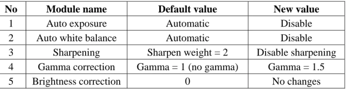
All of these modules can be changed or activated via serial bus control which known as I2C by changing the value of the register in each modules. Although these feature are available inside the chip, but not of these entire feature are activated or changed. It is because some of available function can affect the image that want to be process, such as sharpening function, auto exposure and auto white balance function. The sharpening function can sharpen the edge of the image by changing its value but because the inconsistency of the sharpening edge between image at time t and time t+1, so it can make false motion detection for our optical flow algorithm so we disabled the sharpening module.
Another function that we disabled is the auto exposure time function, by disabling this function the frame rate of the image will be fix although there is any changes of the environment such as lighting changes that coming from the light source so by fixing the frame rate, we can acquire the image from CMOS sensor with a fix frame rate for all the time.
The last function that we disabled is auto white balance function. Activated the function of auto white balance function can also make false motion detection for our optical flow algorithm. It is because when there are any suddenly changing in environment from dark to
white the auto white balance function will try to adapt by changing the R, G and B value to make a new white color for several image frames. In this time, there will be false motion detection even there is no any motion in the image. Generally, the need of motion detection algorithm is that the image must be consistently same for all the time without any suddenly changes so it will be clearly detect motion occur in the image instead of the changing of the environment. Instead of the above module, we also change the gamma correction from the gamma=1 to gamma=1.5 for boosting the darker signal so the image will be brighter. Meanwhile the brightness correction will not be change; it is no necessary to change the value of brightness correction after changing the gamma correction value. The value of the module that has been changed or disabled can be seen in the table 2.1.
Another configuration of the CMOS sensor that should be considered is data output format and data output mode. The ICM205B CMOS sensor offer a various data output format such as: 8/16 bit YCbCr, 24-bit RGB, 16-bit RGB and 8-bit raw data and also output modes such as VGA and its sub-sampling QVGA/QQVGA.
Table 2.1 list of CMOS sensor built in function module that has been changed
No Module name Default value New value
1 Auto exposure Automatic Disable
2 Auto white balance Automatic Disable
3 Sharpening Sharpen weight = 2 Disable sharpening
4 Gamma correction Gamma = 1 (no gamma) Gamma = 1.5
In our embedded image processing platform, we configure the output data as 16-bit YCbCr with the 8-bit low output data is Y and the next 8-bit high output data is sequential output of Cb/Cr which we are just using the 8-bit low output data (Y), so we doesn’t use the 8-bit high output data (Cb/Cr). And for the output data mode, we are using VGA data output mode. The YCbCr data format itself is a similar with YUV color space format which is used in European TVs.
2.3. DSK6416 daughter board
The DSK6416 daughter board consists of two kind interfaces for embedded image processing platform. The first daughter board interface uses for temporary 8-bit image data storage of CMOS sensor data before the image data send to the SDRAM in DSK6416 board. DSK6416 daughter board specification:
z Frame buffer (AL422B): 384 Kbytes
z 7 ports GPIO of DSK6416 for 4 port RS232 emulation
This daughter board uses AL422B from Averlogic Corp [21]. There are several reasons why we choose this frame buffer (AL422B). First, the frame buffer has enough capacity (384 Kbytes) that can store image data up to one image frame (640x480). Second, the speed of the frame buffer is fast enough to operate at 50 MHZ, so it can match with our embedded image processing platform speed that run at 3 MHZ. Third, the control signal of the frame buffer is simple comparable with other similar frame buffer which provide by other company. So the AL422B match with our criteria for temporary image data storage for CMOS sensor data.
The second daughter board consists of 4 COM ports of RS232 interfaces. The need of these 4 COM port of RS232 interfaces are to communicate with other module such as motion card to control motor and IPC. So by having these interfaces, the embedded image processing can run independently to control motor or to communicate with any other module directly. These 4 COM ports of RS232 interfaces emulate from 7 ports GPIO (General Input Output) of the C6416 chip [20]. The emulation use software emulation that writing in the C6416 chip. The software emulation can emulate two ports of GPIO to generate signal RX and TX for one COM port RS232 interfaces signal.
In order to emulate 4 COM ports we need at least 8 ports GPIO, because there are only 7 ports GPIO available so one of the 4 COM ports will have no RX signal which means that one of the 4 COM ports will only have transmit signal (TX) while the other 3 COM ports will have both TX and RX signal. The software emulation can also emulate several baud rates for the COM port RS232 interfaces. The baud rates speed that can emulate by the software emulations are 2400, 4800, 9600, 14400, 19200 and 57600 bps. So within this various baud rate configuration, software emulation can emulate COM port RS232 for several COM port configurations.
2.3.1. Frame buffer (AL422B)
The frame buffer (AL422B) is a video frame buffer consists of DRAM that work like a FIFO which long enough to hold up to 393,216 bytes (384 Kbytes) of picture information and fast enough to operate at 50 MHz [21]. AL422B specification (see figure 2.4):
- Independent read/write operations (different I/O data rates acceptable) - Read/write cycle time: 20ns
- Output enable control (data skipping) - 5 or 3.3. V power supply
From the functional block diagram in figure 2.5, we can see that the frame buffer consists of two kind of separating part that are writing part and reading part. The writing part and reading part have three control signals to be able to write and read data in and out.
These control signals are described as below: 1. Writing part
In the writing part, there are three control signals that control the data from outside that connected to the DI0 … DI7 to be written in to the memory cell array in the frame buffer. These control signal are WCK, /WRST and /WE. The functional of each control signal are:
- WCK (Write Clock)
This control signal is to give a periodic clock to the frame buffer, because the frame buffer memory cell uses DRAM as the storage memory so it required a periodic clock to refresh its data for certain time so the data will still available in
the memory cell array. Instead of refreshing the data in the memory cell, this control signal is used to synchronizing incoming data from DI0 … DI7 to be writing into the memory cell array and will increase the internal counter address memory of the frame buffer.
- /WRST (Write Reset)
This control signal is used to reset the internal counter from current address memory into beginning address memory and active low. Its mean that if we want to write the memory cell array from beginning address, we must to use this control signal to reset the current memory address into the beginning memory address.
- /WE (Write Enable)
This control signal is used to enable the writing operation and active low, so that the data coming from DI0 … DI7 can write into memory array cell.
2. Reading part
In the reading part, there are four control signals that use to read the data out from memory array cell into DO0 … DO7. For the first three control signals, the functional of these control signals will be same as the control signal in the writing part. These three control signals are RCK (Read clock) similar with WCK (Write clock), /RRST (Read Reset) similar with /WRST and /RE similar with /WE. The other control signal that is different with the writing part is /OE (Output Enable).
The functional of the reading part control signal are described as below: - RCK
This control signal is to give a periodic clock to the frame buffer, so the data memory still remains for certain time in the memory cell array, also used to synchronize the data read out from memory cell array into DO0 … DO7 and to increased internal counter address. So when there is an incoming clock into RCK, the data will readout from memory cell array into DO0 … DO7 and after that will increase the internal memory address.
- /RRST
This control signal is used to reset the current internal counter address into beginning address memory and active low. Its mean that if we want to read out the data from beginning address of the memory cell array we must to use this control signal to reset the current memory address back to the starting memory address.
This control signal is used to enable the data to read out from the memory cell array into DO0 … DO7 and active low.
- /OE
This control signal is used to enable reading the data that already available in the DO0 … DO7 and active low. If this control signal is disabling, the output data of the DO0 … DO7 will be in high impendence state.
According to above description of the frame buffer control signal, it is important to give a correct timing for the control signal to write data into frame buffer or to read data out from frame buffer. For this part, we already design the correct timing and it will describe in the following section while describing the FPGA part.
2.3.2. Seven ports GPIO of DSK6416 for emulating four
COM ports RS232 interfaces.
The COM ports RS232 interface in our embedded image processing platform is very important for communication with other modules such as motion control module and PC directly. The C6416 itself does not provide COM port or RS232 interface that support UART standard, but the C6416 provides so-called multichannel buffered serial port (McBSP) that have seven ports that can be configured for General Input Output (GPIO) function [20]. Figure 2.6 shows daughter board for four COM ports RS232 interfaces. So we need to emulate these seven ports GPIO to work as COM port RS232 that supporting UART standard. One way to emulate these GPIO port are using software to emulate it. The software need to emulate two ports of GPIO to act like RX and TX as part of the COM port RS232 interfaces signal which RX for receive signal and TX for transmit signal. To configure the McBSP pins as GPIO, we must configure two registers of the McBSP. These registers are SPCR (Serial Port Control Register) and PCR (Pin Control Register).
The configuration of the McBSP pins as GPIO can be seen at table 2.2 and the block diagram of the McBSP configuration as GPIO can be seen in the figure 2.7. After configuring the seven ports of the GPIO into for four COM ports RS232 interfaces, next we will explain about the software implementation to emulate the TX and RX signal. The software implementation itself has four functions to emulate the COM port RS232 interface. Below is the description of these three functions:
1.) void HR_Initiate_GPIO(void);
This function sets the McBSP in GPIO mode by setting the SPCR and PCR registers according to the table 2.2.
Table 2.2 configuration of McBSP pins as GPIO [20].
Pins GPIO enabled When …
(SPCR register) Selected as Output When … (PCR register) Selected as Input When … (PCR register) CLKX CLKXM = 1 --- FSX FSXM = 1 --- DX /XRST = 0, XIOEN = 1 Always Never CLKR CLKRM = 1 --- FSR --- FSRM = 1 DR Never Always CLKS /RRST = 0, RIOEN=1 Never Always UART McBSP CLKR UART McBSP FSX FSR COM3 UART McBSP DX DR COM4 UART TX RX McBSP CLKX CLKS COM1 COM2 TX TX RX TX RX
Configuration of McBSP pins as GPIO for 4 COM ports RS232 interface
2.) unsigned int HR_SoftUartSpeedDetect(void);
This function of HR_SoftUartSpeedDetect performs Auto-Baud rate detection by measuring the length of the Start bit, plus the length of the first data bit (logic high) by using character <cr> (carriage return = 0x0d). So while this function tries to detect the baud rate, users need to ensure (in software) that the first character sent is <cr> or any other character that the first data bit has to be a logical one. This is shown in figure 2.8. The time T is determined by this function that using a software counter incremented by one until the second transition from high to low is detected (D0) by reading the serial data input (RX). T represent twice the time of the time of a bit length. This measurement is required because the RX signal from UART is not always very clean. Simply measuring the length of the Start bit to determine the baud rate is not accurate enough so we need to use the first data bit which must be at logic high to fix the accuracy. The time reference value UART speed = T/2 is returned from HR_SoftUartSpeedDetect function which this value will use as reference for the Baud rate speed.
The return value of this baud rate will depend on the clock speed of the main processor. In our case, we are using C6416 with 600 MHz, and the return value of this function according to its baud rate speed can be seen in the table 2.3.
Start bit
Stop bit D0
Carriage return character <cr> T = UART speed x 2
Table 2.3 baud rate value detect from HR_SoftUartSpeedDetect function
No
Baud rate speed (bps)
Return value from
HR_SoftUartSpeedDetect function 1 2400 0x144E (5198) 2 4800 0xA27 (2599) 3 9600 0x513 (1299) 4 14400 0x362 (866) 5 19200 0x289 (649) 6 57600 0xD8 (216)
This result is obtaining by transmitting character <cr> from PC to each of the COM ports.
3.) char HR_SoftUartInChar(int BaudRate, int COM_Port);
The HR_SoftUartInChar takes the value of the Baud-rate speeds detected from HR_SoftUartSpeedDetect and select which COM Port that use for receiving the serial data input (RX). Every single 8-bit character read from the serial data input returned from this function. This function parses bit-by-bit the UART data on the serial data input and detects the Start bit by poling the first transition from inactive (logic 1) to active (logic 0) state.
Start bit
D0 D1 D2 D3
P/2 P P
Wait Sample data
Where P = UART speed value Serial data input (RX)
The 8 data bits are transmitted by the UART device immediately after the Start bit. The best time to fetch the right value of each data bit is in the middle of the data bit waveform. Figure 2.9 shows how HR_SoftUartInChar function read out the serial data input. Firstly, it waits for half of the UART speed (P/2) which detected from HR_SoftUartSpeedDetect function during the Start bit. Then for each of the eight valid data bits, it samples the serial data input in the middle of the data bit waveform. Finally this function shifts each binary bit result into a single 8-bit character
4.) void HR_SoftUartOutChar(int BaudRate,char Buffer, int COM_Port);
The HR_SoftUartOutChar function is based on the same mechanism as the HR_SoftUartInChar function. It has had three input arguments, which are Baud-rate speed that detected from HR_SoftUartSpeedDetect function, the single 8-bit character to be sent via serial data output (TX) and last argument is to specify the COM port that one wants to use. At the beginning of a transfer, HR_SoftUartOutChar function writes a logic low (‘0’) to the serial data output as Start bit. Subsequently, it transmits each data bit until 8-bit already send to serial data output. The transmit character is first placed into the least significant 8 bits (LSB) in a register padded with three stop bits (0x00000700).
Start bit D0 D1
Stop bit
1 1 1
P P
Where P = UART speed value Serial data output (TX)
For example, the character ‘A’ with ASCII code is 0x41 will be placed in the padded register to become 0x00000741. Figure 2.10 shows how HR_SoftUartOutChar function sends out the serial data out.
So by emulating the GPIO into COM port RS232 interfaces, there will have more additional COM port RS232 interfaces which will depend on the availability of the GPIO itself. In our case, we can emulate up to four COM ports. But by emulating the GPIO into COM port RS232 interface, the way to receive serial data from other module is not supporting serial port interrupt, so we can just use polling method to receive serial data from other module.
2.4. FPGA (Altera UP2)
Altera UP2
EPM27128S (MAX7000S) -Gate count : 2500 -Max I/O : 104 -EEPROM-based programmable EPF10K70RC240 (Flex10K) -Gate count : 70,000 -Max I/O : 358 -SRAM-based programmableAltera configuration device (EPC1)
The Altera UP2 board (see figure 2.11) consists of two FPGA chips that have different gate counts, and number of I/O (Input and output) [22]. The first FPGA chip (EPM27128S) has 2,500 gate count, max 104 I/O and EEPROM-based programmable. Meanwhile the second chip (EPF10K70RC240) has 70,000 gate counts, max 358 I/O and SRAM-based programmable.
We choose the second chip (EPF10K70RC240) because of the larger gate count and have more available I/O. But this chip (EPF10K70RC240) needs additional boot ROM (EPC1) because of the architecture is SRAM-based
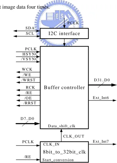
The use of FPGA (Field Programmable Gate Array), Altera UP2 board (see figure 2.11) in our embedded image processing platform is to generate control signals for CMOS sensor, Frame buffer and DSK6416. The design of control signal in FPGA consists of three modules (see figure 2.12). These three modules are I2C, Buffer controller and 8bit_to_32bit_clk.
2.4.1. I2C module
The I2C module is used to generate SDA and SCL signal (I2C signal) in bidirectional input port SDA and SCL to initiate the CMOS sensor (see figure 2.13).
I2C interface PCLK
SDA
Start SCL
I2 C interface Buffer cont roller CMO S SE NS OR (ICM20 5B) PC LK SD A SC L HS YNC /VSYNC D7 ..D0 8 b it Y ima ge da ta Frame buffer (AL4 22B) D7..D0 WC K /W E /WR ST RC K /R E /OE / RRS T 8bit_to_32 bit_ clk St ar t_ co nv er si on CLK _IN Da ta_shift_ clk Sta rt D31..D0 Ex tern al interrupt 7 Ex ter nal interrupt 6 Ext_Int 7 CLK_OUT Ext_Int 6 En hanced DMA con tro ller (E DMA ) (64 chann el ) Ex tern al Memory Inte rface (EMIF ) 32 BIT SD RAM Ch an ne l 0 Ch ann el 2 Interrupt selector FL EX1 0K70R C240 Mult ichanne
l Buffered Serial P
or t 0 (McBS P 0) CO M1 CO M2 CO M3 COM4 2 2 2 L2 M emo ry 64 K by tes JTA G to US B emulati on Host comp ut er USB C641 6 CPU (DS P C ore) L1 P Cache controller L1D C ach e controller DS K6416
Figu
re
2.12
the comp
lete con
trol
sign
al of FPGA
, DSK6
416
an
d CMOS s
ensor
PC L K PCLK /RE SD A SCL PCLK HSYNC /VSYNC Ext_I nt6 Ext_Int 7 TX TX T X TX RX RX RXTable 2.4 configuration of the CMOS sensor
No Feature name Status
1 Auto white balance Disabled
2 Image sharpening Disabled
3 Auto exposure Disabled
4 Gamma correction Gamma = 1.5
5 Data output format 16-bit 4:2:2 YCbCr
6 Data frame rate 30 fps
As we already mentioned in the previous section (section.2.2) the feature of the CMOS sensor can be disabled or enabled by using this I2C module. After completion initiation the CMOS sensor, this module generates a “high” signal in the output port Start to the next module (buffer controller module) to starting to work. The complete configuration of the CMOS sensor that initiates this module is shown in table 2.4.
2.4.2. Clock divider module
The clock divider module (see figure 2.14) that divides the input port CLK_IN by four and
the output can be taken from CLK_OUT and Ext_Int7 output port. Later, “high” signals on
Start_conversion will active this module.
2.4.3. Buffer_controller module
The Buffer_controller module (see figure 2.15) is the main module of the three other modules in the FPGA design. The functional of this module (see figure 2.12) is to read out the correct 8-bit image data from CMOS sensor according to the PCLK, HSYNC and VSYNC control signal. The correct 8-bit image data is then first stored in the frame buffer by generating a correct write control signal (/WE, /WRST, WCK).
After the correct 8-bit image data are stored for a certain time in the frame buffer, the Buffer_controller generates a correct read control signal (/RE, /OE, /RRST, RCK) to read out the 8-bit image data from the Frame Buffer and stored the data in the FPGA. When the 8-bit image data already stored in the FPGA, it is then converted to the 32-bit image data by shifting the 8-bit image data four times.
I2 C in terface
B u ffer co n tro ller
D 7..D 0 R C K /R E 8 b it_ to _ 3 2 b it_ clk S tart_conversion C L K _IN D ata_s hift_clk D 31..D 0 E xt_Int7 C L K _O U T E xt_Int6 P C L K P C L K /R E S D A S C L P C L K H S Y N C /V S Y N C /O E /R R S T /W R S T W C K /W E
After completing shifting the 8-bit image data for four times, the CLK_OUT control signal, that comes from Clock divider module, (see section 2.4.2) tells the Buffer_controller to shift the 32-bit image data [D31 … D0] out from the FPGA.
At the same time, the Clock divider module generates an interrupt signal to C6416 using Ext_Int7 control signal (see figure 2.14) to tell C6416 to fetch 32-bit image data out from FPGA. The last control signal of Buffer_controller is Ext_int6 control signal.
The Ext_Int6 control signal is used to interrupt C6416 that there is an incoming one frame image data. So after receiving this interrupt the C6416 open an EDMA channel to starting fetch the 32-bit image data out from FPGA
2.4.4. Implementation of the Buffer_controller
The implementation of Buffer_controller module is successful that we can acquire image from CMOS sensor for 15 fps and 30 fps. The acquiring methods for 15 fps and 30 fps are different especially in controlling the timing diagram of frame buffer. Next we will discuss these two methods for acquiring images.
2.4.4.1. Acquired image for 15 fps
In the earlier implementation of the Buffer_controller, the way of controlling the frame buffer is divided into two stages; namely, writing stage and reading stage (see figure 2.16). So in the first incoming /VSYNC, the writing stage is active while the reading stage is not active and the next incoming /VSYNC it switches to the reading stage while the writing stage is not
active (see figure 2.16).
Figure 2.16 full timing diagrams for 15 fps configuration
Figure 2.17 timing diagram of Frame Buffer in the writing stage Pixel Clock [D9] Data In [D10] /WE [D1] /WRST [D2] Data Out [D0] /RE or /OE [D5] /RRST [D6] EXT INT7[D3] EXT INT6 [D7] /VSYNC [D8]
The first incoming /VSYNC, and the response of EXT_INT6
Starting to write an 8-bit image-data into frame buffer Pixel Clock [D9] Data In [D10] /WE [D1] /WRST [D2] Data Out [D0] /RE or /OE [D5] /RRST [D6] EXT INT7 [D3] EXT INT6 [D7] /VSYNC [D8] /VSYNC
The writing stage here means that the Buffer_controller enables the writing part control signal of frame buffer to stored 8-bit image data from CMOS sensor for 640x480 pixels (see figure 2.17) by asserting the control signal /WE (/WE=LOW), and disserting /WRST (/WRST=HIGH) which are active low. Meanwhile the reading part of the frame buffer is disabled by disserting the control signal /RE (/RE=HIGH), /OE (/OE=HIGH) and asserting /RRST (/RRST=LOW).
On the other hand, the reading stage here means that in the second incoming /VSYNC, the buffer controller enabled the reading part control signal of the frame buffer to read out 8-bit image data that already stored in frame buffer for 640x480 pixels (see figure 2.18) by asserting the /RE (/RE = LOW), /OE (/OE = LOW) and disserting the /RRST (/RRST = HIGH) control signal. Meanwhile the writing part of the frame buffer is disabled by disserting the control signal of /WE (/WE = HIGH) and asserting /RRST (/RRST = LOW).
Figure 2.18 timing diagram for Frame Buffer in the reading stage Pixel Clock [D9] Data In [D10] /WE [D1] /WRST [D2] Data Out [D0] /RE or /OE [D5] /RRST [D6] EXT INT7 [D3] EXT INT6 [D7] /VSYNC [D8]
The second incoming /VSYNC signal
8-bit image-data is read out from frame buffer (Reading stage)
It is because the Buffer_controller needs two /VSYNC signal to write the 8-bit image data into frame buffer, read it out from frame buffer and move it to the FPGA before it is moved to DSK6416, Therefore the acquire image speed from CMOS sensor until the DSK6416 is
Framerate VSYNC 15fps
2 30 2 / = = =
From figure 2.18, we also can see that in the reading stage, the incoming one image
frame (/VSYNC = LOW), will active EXTINT6 (EXTINT6 = HIGH) signal. Since The
EXTINT6 signal is connected to the interrupt of the C6416 (see figure 2.12) so the active EXTINT6 signal will interrupt the C6416 to tell for an incoming one image frame. Therefore the C6416 enable EDMA channel and open its channel to begin to move 32-bit image data from FPGA to the SDRAM until 640 x 480 by counting EXTINT7 signal.
2.4.4.2. Acquired image for 30 fps
In the second implementation of the Buffer_controller time delay that caused by the switching mode between writing stage and reading stage is reduced that two /VSYNC signals
is reduced to one /VSYNC signal. It means that in the same /VYSNC signal, the switching
mode between writing stage and reading stage occurs (see figure 2.19).
The time difference between writing stage occurs and the following reading stage in one /VSYNC signal (see figure 2.20) is 192 ns or 5.2 KHz. So at the first stage, the Buffer_controller will first store 8-bit image data from CMOS sensor (writing stage) up to 3 x 640 image data into frame buffer by asserting the /WE and disserting /WRST control signal,
EXT_INT6
EXT_INT7
Hsync
Vsync
/ARE/OE
/CE2
D0-D7
An incoming EXT_INT6 signal, to tell C6416 to read out 32-bit from FPGAC6416 response the EXT_INT6 signal by enabled EDMA channel, then 32-bit is read out using EMIF channel 2
EXT_INT7 speed EDMA speed
Figure 2.19 full timing diagrams of writing and reading stage
Figure 2.20 full timing diagram of 30 fps configuration
Pixel Clock [D9] Data In [D10] /WE [D1] /WRST [D2] Data Out [D0] /RE or /OE [D5] /RRST [D6] EXT INT7 [D3] EXT INT6 [D7] /VSYNC [D8] /VSYNC Writing stage and reading stage in one
after that the Buffer_controller activates the reading stage by asserting the /RE, /OE control signal and disserting /RRST control signal to read the 8-bit image data out from the frame buffer to move into FPGA, (before it moves to DSK6416). So at the instant of 192 ns (see figure 2.21), the writing stage and reading stage will run concurrently to write and read the 8-bit data image in the Frame Buffer. According to this new configuration method, the frame rate speed of the acquiring image from CMOS sensor is
fps VSYNC rate Frame 30 1 30 1 / = = = .
The 30 fps frame speed can be reach because there is no additional delay between the writing stage and reading stage in the Frame Buffer.
Figure 2.21 timing diagram for reading and writing stage in 30 fps configuration Pixel Clock [D9] Data In [D10] /WE [D1] /WRST [D2] Data Out [D0] /RE or /OE [D5] /RRST [D6] EXT INT7 [D3] EXT INT6 [D7] /VSYNC [D8]
The different time between writing stage and reading stage
writing stage
Figure 2.22 DSK6416 board with its main list components [19]
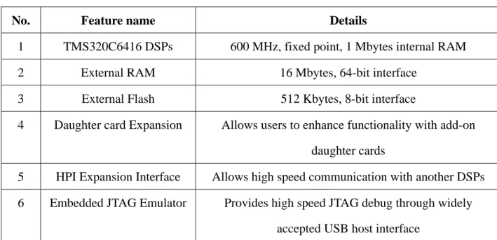
2.5. DSK6416 board
Table 2.5 DSK6416 board specification
No. Feature name Details
1 TMS320C6416 DSPs 600 MHz, fixed point, 1 Mbytes internal RAM
2 External RAM 16 Mbytes, 64-bit interface
3 External Flash 512 Kbytes, 8-bit interface
4 Daughter card Expansion Allows users to enhance functionality with add-on
daughter cards
5 HPI Expansion Interface Allows high speed communication with another DSPs
6 Embedded JTAG Emulator Provides high speed JTAG debug through widely
The DSK6416 is a standalone platform which is equipped with a high-performance DSP chip (C6416), external RAM for a bigger storage solution, external Flash for booting process, daughter card expansion which enabled the DSK6416 to communicate with daughter card / daughter board, with HPI expansion interface to communicate with other DSPs and last Embedded JTAG emulator which enabled the DSK6416 to communicate to Code Composer studio (CCS) while in the development process (see table 2.5) [19]. In our proposed embedded image processing platform, DSK6416 is the main processing platform including
acquiring image from CMOS sensor. Next, we will discuss about software implementation
acquiring image from CMOS sensor into DSK6416 which need a basic understanding about EMIF for interfacing to FPGA that holds 32-bit image data and EDMA controller for selecting an appropriate transfer mode according to the control signal from FPGA.
2.5.1. EMIF (External Memory Interface)
Read data /CE
/OE /ARE ECLKOUT1
Setup Strobe Hold
ED [31..0]
The EMIF is designed for a flexible interface to a wide variety of external memory devices [23]. We use the EMIF as interface to FPGA to read 32-bit image data from FPGA. We treat the FPGA as an asynchronous external memory device which is equivalent to FIFO memory architecture. Figure 2.23 showed the basic asynchronous control signal of EMIF. In order to read 32-bit data through asynchronous interface from FPGA (see figure 2.12), the timing of the EMIF asynchronous control signal must be chosen carefully. The design of required timing can be done by setting the correct setup time, strobe time and hold time for the EMIF timing diagram. In our implementation we choose the correct setup time, strobe time and hold time for the EMIF asynchronous control signal shown in table 2.6.
EXT_INT6
EXT_INT7
Hsync
Vsync
/ARE/OE
/CE2
D0-D7
An incoming EXT_INT6 signal, to tell C6416 to read out 32-bit from FPGAC6416 response the EXT_INT6 signal by enabled EDMA channel, then 32-bit is read out using EMIF channel 2
EXT_INT7 speed EDMA speed
Table 2.6 lists of setup time, strobe time and hold time
No Timing diagram Value (ns)
1 Setup time 60
2 Strobe time 60
3 Hold time 20
In the figure 2.24, the EXT_INT7 control signal shift out the 32 bit image data from
FPGA. We can see that every EMIF control signal (/CE, /OE and /ARE) matches with the
EXT_INT7 control signal. So the correct 32-bit image data are successfully read out from FPGA and will be stored in the SDRAM.
2.5.2. EDMA (Enhanced DMA) controller
The EDMA provides two types of data transfer, 1-dimensional (1D) and 2-dimensional (2D) transfer. The number of dimensions a transfer has determines the makeup of a frame of data. In a 1-D transfer, frames are made up of a number individual element.
0x80030000
Event Triggered (EXT_INT7)
0x8007B000 0xA0000000
CPU
Enabled EDMA7 Channel
ExtInt6 Occured Start _addr
End_adress SDRAM 32-bit FPGA data output
In a 2-D transfer, blocks are made up of a number of arrays, each of which is made up a number of elements. According to our previous implementation of Buffer_controller, the control signal that provided from Buffer_controller is similar to 1-dimensional (1D) transfer. It is because that the output of the Buffer_controller are made up of a number individual which is a individual 32-bit image data with following two control signal that are EXT_INT6 and EXT_INT7. In the figure 2.25, we can see that an incoming EXT_INT6 will tell the CPU that there is one incoming image frame. The CPU then will open EDMA channel 7 that is already directly mapping with the EXT_INT7 signal.
Start
Initial DSK6416
Enable interrupt 6
Initial EDMA for Element Sync Int6 occurred? No Already one frame ? EDMA channel 7 capture 4 pixels Ext Int7 trigger EDMA channel 7 to
capture 4 pixels
Disable Int6 & enable EDMA Channel 7 Yes No Next Image Frame ? Yes Finish Enable interrupt 6 Yes
No
Disable EDMA channel 7
So for every incoming EXT_INT7 interrupt will trigger the EDMA to read out an individual 32-bit image data from the FPGA. And this is repeated until 640 x 480 image data been read out from FPGA. The flowchart of the implementation of EDMA transfer is shown in the figure 2.26.
2.6. Experimental result Image processing
In this section, we show experiment results of acquiring image from the embedded image processing platforms. After acquiring image from the embedded image processing platform, we do a simple processing with the acquired image by using simple algorithm. In the first processing of the image, we use sobel mask to find an edge detection of the image. Later we use image threshold to make a binary image. The embedded image processing platform uses the second configuration with a frame rate of 30 fps. The image resolution is 640 x 480 pixels.
The first experiment is acquired one image frame with 640 x 480 pixels, from the embedded image processing platform. Figure 2.27 show the original image acquired from CMOS sensor. Figure 2.28 shows the original image while applying the sobel mask. Figure 2.29 shows the binary image from thresholding.
Figure 2.27 original image of the CMOS sensor
3 . Visual Servoing
3.1. System architecture
In the early stage of the mobile manipulator research, Connel introduced a behavior-based arm controller in his paper [8]. In his research, Connel combined a multi sensor feedback with the eight loosely-coupled on-board 8-bit microprocessors using behavior-based arm controller. Similar with the work, we propose a motion control for mobile manipulator by combining a behavior-based controller that does not use multiple sensor feedback but only use one visual sensory feedback. The proposed behavior-based algorithm is based on subsumption architecture which is introduced by Brooks [9] (see figure 1.1). The subsumption architecture, control is layered with higher layers subsuming the roles of lower level layers when they wish to take control. The system can be partitioned at any level, and the layers below form a complete operational control system.
In the design of the visual servoing, we choose hand-in-eyes camera configuration to reduced the need for calibrated camera-to-manipulator coordinate transform, and it closed the control loop by providing visual feedback (robot motion caused camera motion) without requiring the vision system to track the end-effector’s (see figure 3.1).
Our proposed algorithm is implemented in the embedded image processing platform for controlling the mobile manipulator robot. The architecture of visual servoing design can be seen in the figure 3.2.
![Figure 1.1 subsumption architecture which introduced by Brooks [9]](https://thumb-ap.123doks.com/thumbv2/9libinfo/8611562.190763/14.892.157.777.861.1035/figure-subsumption-architecture-introduced-brooks.webp)
![Figure 2.4 frame buffer (AL422B) [21]](https://thumb-ap.123doks.com/thumbv2/9libinfo/8611562.190763/33.892.165.788.942.1101/figure-frame-buffer-al-b.webp)
![Figure 2.5 AL422B Functional block diagram [21]](https://thumb-ap.123doks.com/thumbv2/9libinfo/8611562.190763/34.892.131.836.536.1090/figure-al-b-functional-block-diagram.webp)
![Table 2.2 configuration of McBSP pins as GPIO [20].](https://thumb-ap.123doks.com/thumbv2/9libinfo/8611562.190763/38.892.97.837.157.993/table-configuration-of-mcbsp-pins-as-gpio.webp)
![Figure 2.11 Altera UP2 board and its specification [22]](https://thumb-ap.123doks.com/thumbv2/9libinfo/8611562.190763/42.892.115.750.543.1094/figure-altera-up-board-specification.webp)