國 立 交 通 大 學
電信工程學系
碩 士 論 文
考慮製程變異與溫度效應的三維積體電路
功率最佳化方法
Power Optimization in 3D ICs Considering
Process Variations and Thermal Effect
研究生:于斯安
指導教授:李育民 教授
考慮製程變異與溫度效應的三維積體電路
功率最佳化方法
學生: 于斯安 指導教授:李育民 博士
國立交通大學電信工程學系碩士班
摘 要
三維積體電路被視為一個有效的方法來解決二維積體電路上過長導線造成的進步
瓶頸,但是過高的溫度也成為三維積體電路的挑戰。晶片上的溫度會對效能造成
嚴重的影響,因此有必要降低電路的功率消耗。同時,另一個在奈米製程中,對
電路設計有重大影響的議題則是製程變異。在這篇論文中,我們提出一個利用雙
電壓源的統計型方法來降低三維積體電路上的總功率消耗。利用卡洛展開
(Karhunen-Loeve expansion)將通道長度(channel length)和氧化層厚度(oxide
thickness)這類具有空間相關隨機過程的物理參數轉換成一組無相關性的隨機變
數。因為製程變異的關係,晶片上的靜態功率是一個隨機過程,我們利用一個統
計型的溫度分析方法來得到溫度平均值跟變異量的分布。為了強調溫度的影響,
我們採用具溫度相關性的漏電流(leakage current)與邏輯閘延遲(gate delay)模
型,並且完成一套考慮溫度的統計型時序分析方法。所提出降低功率的方法利用
功率延遲敏感度(power-delay sensitivity)作為最佳化的標準,並使用一個以切
格子的(grid-based)方式來處理整個三維積體電路的結構。演算法中使用一個有
效的觀念取代每次的統計型時序分析來增加運作效率。實驗的結果驗證了我們方
法的有效性,並且指出在電路分析中考慮熱效應(thermal effect)是極重要的。
Power Optimization in 3D ICs Considering Process Variations and
Thermal Effect
Student: Shih-An Yu Advisor: Dr. Yu-Min Lee
Department of Communication Engineering
National Chiao Tung University
ABSTRACT
The three-dimensional integrated circuits (3D ICs) have been viewed as an effective methodology to overcome the bottleneck caused by the long interconnects in the 2D IC. However, the higher
temperature becomes a big challenge for 3D ICs. On-chip temperature can significantly affect the circuit performance so it is necessary to reduce the power dissipation in the circuit. Meanwhile, the process variations, which have a serious influence on the circuit design, are another important issue for the nanometer IC design. In this thesis, we present a approach to statistically minimize the total power consumption on the 3D ICs by using the dual supply voltage technology. By Karhunen-Loeve
expansion, the random processes of physical parameters such as the channel length and the oxide thickness with spatial correlations are transformed to a set of uncorrelated random variables. Since the leakage power on the chip is a random process due to the process variations, we employ a statistical thermal simulation method to get the mean and variance of temperature distribution. To emphasize the impact of temperature, the leakage current and gate delay models are temperature related and we implement a thermal aware statistical timing analysis method. The proposed power reduction approach uses power-delay sensitivity as the optimization criterion, and a grid-based method for handling the whole structure of the 3D ICs. Instead of executing statistical timing analysis every time, a potent concept is used in the algorithm to achieve the runtime efficiency. The experimental results demonstrate the effectiveness of our method and indicate that considering the thermal effect in the circuit simulation is imperative.
誌 謝
這篇論文能夠順利地完成,首先要感謝我的指導教授 李育民博
士,當我遭遇困難時,老師總會適時指引我方向,讓我能夠繼續前進。
兩年的學習過程中,老師的訓練和指導給了我莫大的幫助,讓我確實
感受到自己的成長,我相信這對我未來不管是工作或進修都會有相當
大的幫助。
實驗的部份,感謝周景揚老師提供我們聯電 90 奈米製程參數,感
謝鍾菁哲博士和陳志龍學長在實驗設定的協助,感謝 Renato 教授提
供的軟體,感謝 Markov 教授對實驗流程的指導,還有同儕建螢給予
的幫助,沒有你們,要完成這個實驗是相當困難的。我在此對你們至
上最大的謝意。
在實驗室裡,感謝培育學長和柏毅學長在知識與技術方面的指導
與傳承,以及國富、志康、炳熏、至鴻、佳鴻、懷中、庚達、宗祐、
阿文給予的關心與幫助,同窗焯基的相互勉勵,豐富這二年的生活。
特別感謝好友宣聆,給予我許多支持與鼓勵,陪伴我度過最低潮
的日子。
最後要深深地感謝我的父母,你們無微不至的照顧並且提供安穩
的環境讓我可以毫無顧慮地在學業上衝刺,讓我能夠順利完成碩士學
業。僅在此將本論文獻給你們,共享這份喜悅與榮耀。
Contents
1 Introduction 1
1.1 Introduction . . . 1
1.2 Our Contributions . . . 3
1.3 Organization of the Thesis . . . 3
2 Preliminaries 4 2.1 3D IC Technology . . . 4
2.1.1 Motivation for 3D ICs . . . 4
2.1.2 Benefits and Challenges of 3D Integration . . . 5
2.1.3 Current 3D Technology . . . 5
2.2 Parameter Modeling . . . 7
2.2.1 Karhunen-Loeve Expansion . . . 7
2.2.2 Spatial Correlation Modeling . . . 8
2.3 Statistical Leakage Current Modeling . . . 9
2.3.1 Gate Tunneling Leakage Current . . . 9
2.3.2 Subthreshold Leakage Current . . . 10
2.4 Timing Analysis . . . 11
2.4.1 Static Timing Analysis (STA) . . . 11
2.4.2 Statistical Static Timing Analysis (SSTA) . . . 12
2.5 Power Optimization . . . 13
2.5.1 Statistical Leakage Power Optimization and Deterministic Dynamic Power Optimization . . . 14
2.5.2 Multiple Supply Voltage (MSV) Technique . . . 14
2.5.3 Previous Works of Post-Placement Voltage Island . . . 16
3 Statistical Power Optimization in 3D ICs 17 3.1 Problem Formulation and Flowchart . . . 17
3.2 Statistical 3D Thermal Analysis . . . 18
3.2.1 Thermal Model of 3D IC . . . 19
3.2.2 First Stage . . . 19
3.2.3 Second Stage . . . 20
3.3 Temperature Aware Statistical Timing Analysis . . . 20
3.4 Voltage Island Generation in 3D ICs . . . 23
3.4.1 Voltage Assignment . . . 23
3.4.2 Incremental Update . . . 27
3.4.3 Site Rescue . . . 28
3.4.4 Post Tuning . . . 30
4 Experimental Results 32
5 Conclusion 38
A Statistical Thermal Simulation 50
A.1 Polynomial Chaos . . . 50
A.1.1 The Bases for Random Space . . . 51
A.2 Stochastic Galerkin Procedure . . . 52
A.3 Gate Leakage Power Projection . . . 53
List of Figures
1.1 Leakage variations [18] . . . 2
2.1 Assembly process for a 3D chip [38] . . . 6
2.2 An example illustrating the application of the STA. The numbers within the block correspond to the delay of the block. The primary inputs are assumed to be available at time zero. . . 12
2.3 (a) Design with timing-critical cells (small purple cells). (b) Power consump-tion too high. (c) Timing requirement not met for small cells in module A. (d) Placement-proximity-based solution with nonlogical boundary. . . 16
3.1 Flowchart of the proposed statistical power optimization for 3D ICs . . . 17
3.2 The schematic diagram of a 3D IC with 3 chip layers . . . 18
3.3 The schematic diagram of a 3D IC with Nlchip layers . . . 19
3.4 Algorithm of the statistical thermal simulation. . . 21
3.5 A three-tier chip example for constructing the experimental model of power density induced weights. (a) An 1W power is inserted into the grid (5, 5) on the tier 1 and the corresponding temperature profile on each tier. (b) An 1W power is inserted into the grid (5, 5) on the tier 2 and the corresponding temperature profile on each tier. (c) An 1W power is inserted into the grid (5, 5) on the tier 3 and the corresponding temperature profile on each tier. The color bar shows the related levels of the temperature with respect to the colors on tiers. The arrows indicate the 1W power sources. The rectangles with dotted line margins are the truncation regions. . . 25
3.6 A three-tier design example of the grid-based procedure for generating the volt-age islands. Each tier is first divided into many grids, and the grid with the high sensitivity has dark color. After compressing, the criteria are accumulated, the higher priority the grid has, the darker the color is. When the grid with the high-est priority is found, it is rhigh-estored to the multi-layer structure to decide which tier should operate at the low supply voltage. . . 27
3.7 (a) Initial state. (b) The low supply voltage is assigned to gate A, but the AT of gate C is not affected. (c) The low supply voltage is assigned to gate A, and the AT of gate C is affected. (d) Statistical form. . . 29
3.8 The grids with dark color operate at low supply voltage and the grids with light colors operate at high supply voltage. The red block is the site and the blue block is the replacer. . . . 29
3.9 Voltage Island Extension . . . 31
4.1 Temperature impact on slack distribution. . . 33
4.2 (a) Voltage assignment result on layer 1. (b) Voltage assignment result on layer 2. 36 4.3 (a) Voltage islands on layer 1. (b) Voltage islands on layer 2. . . 36
4.4 (a) Initial temperature distribution on layer 1. (b) Optimized temperature
distri-bution on layer 1. . . 37
4.5 (a) Initial temperature distribution on layer 2. (b) Optimized temperature
distri-bution on layer 2. . . 37
List of Tables
4.1 Leakage Power Estimation . . . 34
Chapter 1
Introduction
1.1
Introduction
As consumer demands on integrated circuits increase, the interconnect structure has become the bottleneck of the chip performance. Increased interconnection lengths produce serious par-asitic effects which increase the circuit delay and the power consumption. Three-dimensional integrated circuits (3D ICs) have been proposed to solve this problem. The 3D ICs allow the designer to stack dies or wafers vertically in the same package and connect components on the different tier by through-silicon vias (TSVs) [1]. However, the heat removal is an important issue in the 3D IC design due to the higher power density and the low thermal conductiv-ity inter-layer dielectrics between the device layers. The high temperature can reduce the life time and reliability of device and impact the circuit performance in the timing and leakage power [2, 3, 4, 5]. Numerous researches have been done in the physical design level to handle the temperature problem. Floorplanning [6, 7], placement [8], routing [9, 10, 11], and thermal via insertion [12, 13, 14] are used to arrange the power distribution and improve the thermal con-ductivity on the chip. However, if the designer wants to solve this issue fundamentally, making power reduction is a necessary step since the power consumption in the circuit is the source of thermal problem. In addition, due to the shrinking of device geometries, it is more difficult to control the device parameters. Growing process variability such as the effective channel length, the gate oxide thickness, the ILD thickness, the random doping concentration and the threshold voltage has made the deterministic analysis and optimization at a prescribed process corner be no longer effective. The traditional approaches can significantly overestimate or underestimate the impact of process variations. Overestimation leads to increased design time/effort and
re-sults in the performance loss while underestimation causes the yield loss. As shown in [15], 30% process variations can cause up to 20X leakage power variations. According to ITRS, the ratio of the leakage power to the total power has increased 10 times from the 180 nm process to the 90 nm process [16]. Furthermore, at the 90 nm process nodes, leakage power accounts for 25% to 40% of the total power, and it is expected that 50% to 70% of the total power will be lost through the leakage currents at the 65 nm process [17]. Hence, it is imperative to consider process variations in the power optimization work.
1.2
Our Contributions
In this thesis, a power minimization methodology for 3D ICs is presented; the main contribu-tions of the thesis are summarized in the following terms:
• We propose a power optimization approach for the 3D IC design which considers process
variations and thermal effect to the timing and leakage power by using the dual supply voltages. Compared with the previous works which solve the deterministic problems and use the thermal unrelated models, our method is more flexible and practical. Furthermore, this is the first work that discusses the voltage island generation in 3D ICs.
• Besides the physical parameters such as the channel length and the oxide thickness, the
temperature is treated as a variation parameter in the statistical static timing analysis (SSTA). A similar idea can be found in [19]. In that work, the temperature is assumed to be independent of the circuit design and the temperature on each location is equal; however, the placement of circuit can affect the power distribution, and the leakage power is impacted by the physical parameters. Therefore, the temperature should be viewed as a random variable which is a function of physical parameters to get a reasonable answer.
• No matter what method is used, the timing information of the circuit should be updated
af-ter each step or adjustment. The proposed algorithm uses a heuristic and efficient method to avoid the expensive cost of SSTA.
1.3
Organization of the Thesis
The organization of the rest of the thesis is as follows. Chapter 2 gives an overview of the nec-essary background for this work, including 3D IC technology, parameter modeling, Karhunen-Loeve expansion, leakage current modeling, statistical timing analysis, and the multiple supply voltage technique. Our experiment flowchart, statistical 3D thermal analysis, thermal aware statistical timing analysis, and power optimization method are addressed in chapter 3. Finally, the experimental results and conclusion are presented in chapter 4 and 5, respectively.
Chapter 2
Preliminaries
In this chapter, we first study the background knowledge of 3D IC. Second, the parameter modeling is presented in section 2.2. After that, we introduce the statistical leakage current modeling in section 2.3. The next section surveys the methods of static timing analysis and statistical timing analysis. Finally, some power optimization works are reviewed and the idea of post-placement voltage island is presented.
2.1
3D IC Technology
2.1.1
Motivation for 3D ICs
The unprecedented growth of the computer and the information technology industry are de-manding very large scale integrated (VLSI) circuits with increasing functionality and perfor-mance at minimum cost and power dissipation. While the VLSI technology scales down, the circuit improvement is limited by the long interconnect. The long interconnect on 2D chip causes serious parasitic effects which slow down the circuit speed and require an increasing number of inserting buffers. The increasing interconnect loading also affects the power con-sumption in high-performance chips. On-chip global wires contribute about 34% to the total chip power dissipation in an Intel microprocessor [20]. Additionally, it results in other prob-lems such as signal integrity and routing congestion. Furthermore, increasing drive for the inte-gration of analog/digital signals and disparate technologies introduces various system-on-chip design concepts, for which existing planar IC design may not be suitable.
2.1.2
Benefits and Challenges of 3D Integration
3D ICs replace the long interconnect on 2D chip by the shorter vertical vias which can lead to over 25% decrease in the worst case wire length [21, 22]; at the same time, the interconnect power [23] and the chip area are also reduced [1]. This is especially important for proces-sors as they access memory continuously. With 3D integration, the access time is reduced, and the system performance is improved. This improvement has been studied in many re-cent works [24, 25, 26]. In addition, 3D ICs allow the integration of different technologies such as memory, logic, RF and analog components on one chip. IC technologies in differ-ent active device tiers wouldn’t face the technology and manufacturing incompatibilities and cross-contamination issues. Other advantages include reduced power consumption, increased packing density, decreased packaging size, weight, and cost. However, 3D integration has its own challenges in terms of fabrication, production yield, heat removal and process varia-tions [27, 28, 29, 30]. Both the fabrication process and production yield are highly related to the through-silicon vias. Making these vertical vias is a complicated and difficult procedure in the design flow. On the other hand, due to the higher power density and the low thermal conduc-tivity inter-layer dielectrics between the device layers, 3D ICs have a much higher temperature than 2D ICs. As shown in [29], the gate delay has a linear relation with the temperature and the leakage power has an exponential relation with the temperature. In brief, the temperature effect is an undeniable factor in the circuit simulation.
2.1.3
Current 3D Technology
3D IC fabrication technologies include multi-chip module (MCM) packaging, wafer bonding, solid-phase recrystallization, etc. Different fabrication technologies can greatly affect the circuit performance, manufacturing cost, on-chip temperature, etc. Wafer bonding is the most popu-lar method currently. In wafer-level 3D integration, functional materials and components are prefabricated on separate wafers, followed by wafer aligning, bonding, and vertical inter-wafer interconnection to integrate these functional materials and components in a 3D stack. There are three main methods to achieve wafer-scale 3D integration [31]: wafer-to-wafer, die-to-wafer,
Die-to-wafer uses a substrate wafer to integrate an already diced die on top of it. Die-to-die integration allows the same high yield as die-to-wafer but suffers from low-production through-put. Recent developments toward reliable and high yield adhesive bonding processes have made adhesive wafer bonding a good candidate for 3D integration platforms. In adhesive wafer bond-ing, an intermediate adhesive polymer layer is used to create a bond between two wafers. The main advantages of adhesive bonding are the compatibility with integrated circuit wafers, the relatively low bonding temperatures, the ability to join practically any kind of wafer material and an insensitivity to particles and structures at the wafer surfaces. In most commonly used adhesive wafer bonding processes, the polymer adhesive is applied to one or both of the wafer surfaces to be bonded. Often, the polymer coatings are heated after spin-coating to remove sol-vents and/or to partially cross-link the polymer coating. After aligning two wafers and joining the polymer-coated surfaces, pressure is applied to fore the wafer surfaces into intimate con-tact [32]. The topics about the application and design flow can be found in [33, 34, 35, 36, 37]. The assembly process and a 3D chip consisting of three tiers are illustrated in Fig. 2.1.
2.2
Parameter Modeling
Process variations can be classified into inter-die variations and intra-die variations. Inter-die variations are the variations from die-to-die. All the cells in one die have the same variation type. On the other hand, intra-die variations correspond to the variability within a single chip. With continuous process scaling, intra-die variations have to consider the spatial correlation which the devices with close proximity are more likely to have similar process parameter values.
2.2.1
Karhunen-Loeve Expansion
Considering the spatial correlation of intra-die process variations is a significantly challenging task because of the severely increased variables and computational complexity. The physical parameter on one location is a random variable while all the parameters on the chip become a random process. Thus, we need infinite random variables to accurately model the spatial correlation on the chip. It is complicated and impossible. An alternative method is the use of Karhunen-Loeve (KL) Expansion. The concept of KL expansion is to find a set of mutually independent random variables as the bases for the on-chip variations, and express the physical parameter on any location as the combination of these bases. Hence, the original large number of correlated random variables can be modeled by the small number of uncorrelated random variables, which can reduce the complexity and improve the efficiency. The set size is decided by the user to control the approximation error. Moreover, the chip can be divided into many grids and the center point of each grid can be the reference point for computing the covariance value and distance. Therefore, all the gates in the same grid can share the same coefficients and the number of grids is relatively small compared with the number of gates on the chip.
The KL expansion of a second-order random process α(x, y, z, ϑ) with a continuous spatial covariance function is expressed as follows [39]
α(x, y, z, ϑ) = α(x, y, z) + ∞ X k=1 √ γkφk(x, y, z)ηk(ϑ), (2.1)
where α(x, y, z) is the mean value of α(x, y, z, ϑ), and each γk and each φk(x, y, z) are the
eigenvalue and the eigenfunction derived from the following Fredholm integral equation
Z
D0
Here, C(x1, x2) is the covariance function of the random process α(x, y, z, ϑ), x1 = (x1, y1, z1)
and x2 = (x2, y2, z2) are locations, ϑ is the sampling event of the sample space Ωα, and {ηk(ϑ)}
is a set of uncorrelated random variables with each ηk(ϑ) being zero mean and unit variance. In
contrast to the conventional 2D IC, we add the z- dimension to represent the tiers of 3D IC. With the spatial covariance function, physical parameters such as the effective channel length and the gate oxide thickness can be modeled as random processes. It has been indi-cated that, for the covariance function of a physical parameter, the statistical covariance at two different points decreases as the distance between these two points increases [40]. Functions like the exponential form, the Gaussian form, the linear form, or a fitting form with experi-mental data are suggested to model this property [41, 42, 43]. By the use of the second-order property and the above covariance functions, the KL expansions of the physical parameters are valid.
2.2.2
Spatial Correlation Modeling
Researchers in [44] presented that the decreasing rate of the spatial covariance of physical pa-rameters is different in the x- and y- directions on the chip. The following spatial covariance function is adopted to model this characteristic
C(x1, x2) = σ2exp − |x1− x2| ηx ! exp −|y1− y2| ηy ! , (2.3)
where ηxand ηyare correlation lengthes of the target random process in the x- and y- directions,
respectively, σ is the standard deviation of the target random process, and this covariance kernel
is defined in the rectangular domain D0. Because the process variations on different tiers are
mutually independent [30], the function does not consider the z- dimension and can still be utilized.
With the above function, the KL expansions of gate oxide thickness (tox(x, y, z, $)) and the
effective channel length (Lef f(x, y, z, θ)) can be obtained as
tox(x, y, z, $) ≈ tox(x, y, z) + 4tox(x, y, z, $), (2.4)
and 4tox(x, y, z, $) ≡ Ntox X n=1 q βnfn(x, y, z)ςn($), (2.6) 4Lef f(x, y, z, θ) ≡ NLeff X m=1 √ χmqm(x, y, z)ζm(θ). (2.7)
where tox(x, y, z) and Lef f(x, y, z) are the expected values of tox(x, y, z, $) and Lef f(x, y, z, θ),
fn(x, y, z) and qm(x, y, z) are eigenfunctions of tox(x, y, z, $) and Lef f(x, y, z, θ), βnand χm
are eigenvalues of tox(x, y, z, $) and Lef f(x, y, z, θ), respectively. The Ntox and NLef f are
the truncated numbers of tox and Lef f. {ςn($)} and {ζm(θ)} are mutually independent
stan-dard normal random variables since tox(x, y, z, $) and Lef f(x, y, z, θ) can be assumed to be
Gaussian processes [45], and they are assumed to be independent. Here, we use {ξn($, θ)}Nn=1KL
as the union of {ςn($)}Nn=1tox and {ζn(θ)}
NLeff
n=1 , NKL = Ntox + NLef f and ξn, ςnand ζnare used
to represent ξn($, θ), ςn($) and ζn(θ) for simplicity in the following content.
2.3
Statistical Leakage Current Modeling
In this section, we introduce the empirical models for subthreshold and gate leakage currents with the uncertainty in physical parameters such as channel length and oxide thickness. Ac-tually, the leakage currents depend on the input pattern and logic topology. We evaluate the average leakage currents based on H-SPICE simulation for various types of logic gate with in-put pattern considered. From the H-SPICE simulation results, we obtain the fitting constants of the empirical current models based on the least square method. The maximum errors of fitting models are no more than 2% in comparison with the H-SPICE simulation results. Because the leakage current is supply voltage dependent, we fit two pairs of coefficients corresponding to the high/low supply voltages.
2.3.1
Gate Tunneling Leakage Current
According to quantum mechanics, there is a finite probability that carriers can tunnel through the gate oxide. The result is so-called that the gate tunneling leakage current flows into the gate. The finite probability is an exponential function of oxide thickness. The gate tunneling leakage current increases exponentially as oxide thickness decreases. When the oxide
thick-ness is thicker than 20 ˚A, the gate tunneling leakage current is relatively small in comparison
with other leakage currents such as the subthreshold leakage current. For the oxide thickness
is thinner than 15−20 ˚A, the tunneling current becomes an important factor and may become
comparable with the subthreshold leakage current in advanced process. To put it briefly, the dependence of gate leakage current on oxide thickness is given by the following formula [46]:
Igate = (A · C)(W · L)e −B·tox Vgsα, where A = q3/8πhφb, B = 8π √ 2moxφ 3/2 b /3hq, C = (Vgs/tox)2, α is a parameter which is
ranged from 0.1 to 1 depending on the voltage drop across the oxide, H is the Plancks constant,
and φb is the barrier height for electronics/holes in the conduction/valance band. Note that the
parameter variations are in general around 10-20% [47]. Hence, we make use of a first-order Taylor expansion at the nominal value of parameter oxide thickness and utilize the following gate tunneling leakage current model derived in [48].
Igate= b0exp(b1tox), (2.8)
where b0 and b1 are fitting constants, tox is the oxide thickness. Because the parameter Vgs is
related to the supply voltages, we fit two pairs of coefficients for the high/low supply voltage, respectively.
2.3.2
Subthreshold Leakage Current
The subthreshold leakage current is defined as the conduction current between source and drain in an “off” state CMOS transistor. The subthreshold leakge current for a MOSFET can be modeled as [49] IOF F = Ids = µef fCox Wef f Lef f (m − 1)VT2(1 − exp(−Vds VT ))exp(Vgs− Vth mVT ), (2.9) m = 1 + q εsiqNa/4ΨB Cox ,
where µef f is the effective mobility, Cox is the gate-oxide capacitance, Lef f is the effective
channel length, Wef f is the effective width, VT is the thermal voltage, Na is the channel
difference between Fermi potential and intrinsic potential. Here, we still use the first-order for-mulation and consider the temperature impact [29], so the subthreshold leakage current model is
Isub= c0exp (c1Lef f + c2T ) , (2.10)
where c0, c1 and c2 are fitting constants, Lef f is the channel length and T is the temperature.
As the gate leakage current, we fit two pairs of coefficients due to the relation between Vgs and
supply voltage.
2.4
Timing Analysis
2.4.1
Static Timing Analysis (STA)
Before introducing the SSTA, we first review the traditional STA and several basic knowledge. In timing analysis, each gate has three types of timing information: 1) arrival time (AT) 2) re-quired time (RT) 3) slack. The AT means the real time that the signal arrives; the RT represents the designer’s constraint that when the signal should arrive. The definition of slack is the differ-ence between AT and RT. When the slack is positive, which means that the signal arrives earlier than the designer’s request, there is no timing violation. The gate with positive slack can be optimized to reduce the circuit’s area or power dissipation.
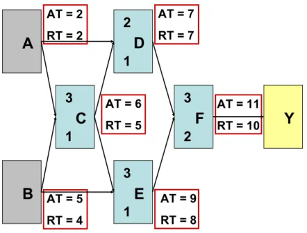
Now we use the example shown in Fig. 2.2 to describe the details of STA. The method that is commonly referred to as PERT (Program Evaluation and Review Technique) is popularly used in STA [50]. In this figure, each block could be as simple as a logic gate or a more complex combinational block, and is characterized by the delay from each input pin to each output pin.
A and B are the primary inputs; Y is the primary output. Initially, a depth first search (DFS)
is performed and the blocks are put into a queue according to their sequence. Generally, it is assumed that all primary inputs are available at time zero. Hence, the AT of the output of
A is simply the delay of A, so does B. Then, for C, it has two different inputs A and B. The
AT from A is computed as 2+3=5; while the AT from B is computed as 5+1=6. Since the timing analysis considers the worst case, the AT of the output of C should choose the latest one, which is the maximum of 5 and 6. Doing a forward traversal, we can get the arrival time of all blocks in the circuit. On the other hand, the RT is calculated by a backward traversal from
A
B
D
E
C
F
Y
3
1
3
2
3
1
2
1
AT = 2 RT = 2 AT = 5 RT = 4 AT = 7 RT = 7 AT = 9 RT = 8 AT = 6 RT = 5 AT = 11 RT = 10Fig. 2.2: An example illustrating the application of the STA. The numbers within the block correspond to the delay of the block. The primary inputs are assumed to be available at time zero.
the primary output. The RT at the output of F is 10, which is set by the designer. Then the RT of D and E are computed as 10-3=7 and 10-2=8, respectively. After the computation of AT and RT, we can get the slack of each gate by subtracting the AT from RT. The critical path, which is defined as the path between an input and an output with the maximum delay, is the path B-C-E-F-Y. In the above example, the delay time of each gate can be searched in the cell library. The conventional method builds the library according to several process parameters and tries to make the design work under the defined worst situation. Unfortunately, in presence of process variations, the traditional STA is pessimistic and not effective. The increasing variation parameters make it complex and impractical to build such a huge library. Moreover, from the viewpoint of probability, the possibility of worst case is extremely small.
2.4.2
Statistical Static Timing Analysis (SSTA)
The alternative approach in timing analysis is the SSTA which treats delays as random variables and propagates the random variables in the circuit. Existing SSTA methods can be categorized into two approaches: the path based SSTA and the block based SSTA. The path based SSTA tries to find the statistical critical paths. However, the task of selecting several timing critical
paths statistically has high complexity that grows exponentially with respect to the circuit size. On the other hand, the block based SSTA treats each gate/wire as a timing block and performs the timing analysis block by block in the circuit timing graph without looking back to the path history. Hence, the computation complexity would only grow linearly with losing part of accuracy.
Numerous literatures have investigated the SSTA in various directions. Many researchers suggest the variations to be Gaussian random variables and use the canonical first order formu-lation to represent the delay [51, 52, 53, 54]. In contrast, various studies assume the fluctuations to be Gaussian distributions [55, 56, 57] or probabilistic interval variables [58] and use non-linear delay functions [59]. How to reduce the error caused by the MAX operation is proposed by [60], and how to take the spatial delay correlations into account is introduced in [61]. How-ever, authors in [62] indicated that considering the parameters as Gaussian random variables and the use of linear delay model can provide sufficiently accurate simulation. Hence, we follow this assumption in our experiment.
2.5
Power Optimization
In this section, we review several previous publications about power optimization and introduce our utilized method. Power dissipation in CMOS digital circuits consists of dynamic power, short circuit power and leakage power. The short circuit power is usually negligible compared to dynamic power and leakage power. Therefore, most of the optimization works focus on the latter two sources of power consumption. Generally, the dynamic power is insensitive to process variations and can be assumed to be deterministic [63]. The leakage power is greatly affected by physical parameters with uncertainties because of manufactured process variations, and needs to be treated as random processes. Existing useful power reduction methods at the circuit-level are the supply voltage scaling, threshold voltage scaling, gate-oxide scaling, gate-sizing, retiming, and any combination of these methods.
2.5.1
Statistical Leakage Power Optimization and Deterministic Dynamic
Power Optimization
A performance optimization based on the criticality is proposed in [64]. By modeling the sta-tistics of leakage and delay as posynomial functions, authors in [65] formulate a geometric programming problem and solve it by the convex optimization method. In [66], it is formulated as an unconstrained nonlinear optimization problem and solved based on the efficient power and delay gradient computation. A statistical power optimization algorithm under the timing yield constraint is presented in [67], where the second order cone programming is employed. Some sensitivity-based heuristic methods are proposed to reduce the leakage power [68, 69]. The above works utilize the techniques of gate-sizing and dual-threshold voltage to reduce the leakage power statistically. However, most of them neglect the importance of dynamic power.
On the other hand, many researches use the multiple supply voltages to do the deterministic dynamic power optimization [70, 71, 72, 73, 74, 75, 76, 77, 78, 79, 80, 81, 82, 83, 84]; never-theless, the leakage power is ignored in their experiments. Although several studies consider the dynamic and leakage power at the same time, they still have their limitations. Authors in [85] propose an algorithm based on the linear programming. The genetic algorithm is employed in [86] to do the power optimization. A two-phase flow is presented in [87] to minimize the power consumption. By the use of retiming and Vdd/Vth scaling, the authors [88] formulate the problem by using the integer linear programming approach. These studies are all determin-istic methods. Although the work in [67] considers the total power reduction statdetermin-istically, it does not take the temperature influence into account.
2.5.2
Multiple Supply Voltage (MSV) Technique
The concept of MSV method is to assign lower supply voltages to gates on the non-critical path for power saving and assign higher supply voltages to gates on the critical path for satisfying the timing constraint. It provides the premium result with less penalty [89]. The two constraints introduced by the MSV method are the electrical constraint and the physical constraint. In a voltage-scaled circuit, if a low supply voltage gate drives a high supply voltage gate, a level converter (LC) must be inserted to eliminate the undesirable static current. The additional level converters would increase the cost in area, delay and power; hence, the number of level
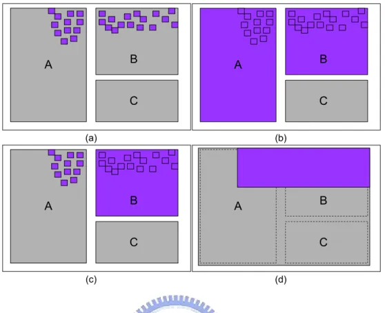
convert-ers must be controlled. Moreover, cells operating at different supply voltages should be placed carefully to facilitate the power network design and reduce the routing complexity. Previous efforts toward reducing the level-shifting overhead include: 1) clustered voltage scaling (CVS) and 2) extended CVS (ECVS). The CVS partitions a circuit into two clusters - one having only cells operating at high supply voltage and the other having only cells operating at low supply voltage. The scenario in which a cell driven by low supply voltage directly feeds a cell driven by high supply voltage is clearly precluded in this partition. The ECVS relaxes this topological constraint and allows a cell with low supply voltage to feed a cell with high supply voltage after its output has undergone level conversion. Thus, ECVS has more freedom in finding parts of the circuit that can be operated at the lower supply voltage and can potentially lead to higher power saving. However, the delay penalty tends to be larger too. An effective solution is grouping cells of different supply voltages into a small number of “voltage islands”, where each voltage island occupies a contiguous physical space and operates at a single supply voltage and meets the performance requirement.
Logic boundaries are largely used in this grouping process mainly because they are the boundaries that designers are most familiar with. Nevertheless, these natural boundaries in a design are almost always nonoptimal boundaries for supply voltages. Fig. 2.3 illustrates why sticking to logic boundaries is limiting the solution space in producing optimal MSV. In the example, there are three modules, each of them contains only leaf cells, and both modules A and B contain some timing-critical cells that require high voltage Fig. 2.3(a). Fig. 2.3(b) and (c) are the designs based on logic boundaries. While Fig. 2.3(b) guarantees the performance using high power, Fig. 2.3(c) reduces the power consumption without meeting the timing requirement. None of them are optimal MSV. By using placement proximity (instead of logic) information, the optimal MSV meets power and timing requirements at the same time while keeping the number of power domains small as shown in Fig. 2.3(d). This idea is called post-placement voltage island generation [72]. Due to the advantages of the post-placement voltage island, we employ this methodology in our experiment. Another reason is that the location of each gate is provided in the post-placement stage so the spatial correlation can be considered in the SSTA.
A B C (a) A B C (b) A B C (c) A B C (d)
Fig. 2.3: (a) Design with timing-critical cells (small purple cells). (b) Power consumption too high. (c) Timing requirement not met for small cells in module A. (d) Placement-proximity-based solution with nonlogical boundary.
2.5.3
Previous Works of Post-Placement Voltage Island
The post-placement voltage island can be performed in two stages: supply voltage assign-ment [73] and voltage island generation [72]. Using the concept of the zero slack algorithm and the Voronoi diagram, authors in [73] propose a proximity-driven-voltage-assignment algorithm. Based on the placement and the voltage requirement of each cell, they continue implementing an efficient algorithm to find the voltage islands for the best tradeoff between the total power and the number of islands [72]. The method developed in [74] allows the generated voltage islands to be any shape instead of only rectangular [72].
Chapter 3
Statistical Power Optimization in 3D ICs
Netlist Cell Library ( LEF/DEF )
Timing/Leakage
Power Cell Library 3D Placement ( Bookshelf )
Statistical 3D Thermal Analysis Thermal Aware Statistical Timing Analysis
Timing
Violation Yes Rescue No Timing Yes 3D IC Voltage Budget No Voltage Assignment Post Tuning Grouping and Extension Grouping and Extension
End
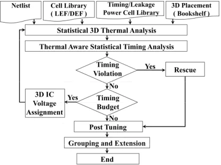
Fig. 3.1: Flowchart of the proposed statistical power optimization for 3D ICs
3.1
Problem Formulation and Flowchart
The proposed power reduction design flow for 3D ICs is shown in Fig. 3.1. Given a known placement, design netlist and a standard cell library, the flow first executes a statistical thermal simulation to obtain the statistical temperature distribution for the specified 3D IC. After that, a thermal aware SSTA is performed with the statistical temperature distribution got from the previous step. The slack data provided by SSTA is used to compute the power-delay sensitivity; next, a grid-based procedure is developed for the voltage assignment. After the assignment procedure, the power consumption and delay of gates are changed so we do the thermal and
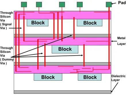
Block Block Block Block Block Pad Dielectric Layer Metal Layer Through Silicon Via ( Signal Via ) Through Silicon Via ( Dummy Via )
Fig. 3.2: The schematic diagram of a 3D IC with 3 chip layers
timing analysis again, and the timing of the circuit is verified. If there is any timing violation, a rescue procedure is enforced to assure the timing correctness and finish the iteration. When the circuit satisfies the timing constraint, the program starts the assignment process again. The program also terminates the loop when the iteration can not provide more improvement. Then, a post-tuning step is employed to further lower the power consumption. In the last process, the proposed method uses grouping and extension to implement the voltage island generation. Each executing step will be described in the following sections.
3.2
Statistical 3D Thermal Analysis
The utilized statistical electro-thermal aware 3D IC thermal simulator extends the Hermite poly-nomial chaoses (H-PCs) based 2D IC statistical thermal simulator [90, 91] to the 3D IC, and combines the developed 3D IC statistical thermal simulator with the electro-thermal iterative updating loop. The details of the algorithm are presented in the Appendix A. The entire ther-mal simulation flow is summarized in Fig. 3.4. The simulation can be divided into two stages; we introduce the contents of the method in the following subsections.
1 , , , p x y z t
2Nl1 , , , p x y z t Silicon Layer…
1, 1 2Nl1, 2Nl1 2Nl2, 2Nl2 Insulator Layer 2 d 2Nl 2 d Z z L 0, 0 0 z Insulator Layer Chip Layer Nl-1 Chip Layer 0 xL
…
Silicon Layer Silicon Layer 1 d 2Nl1 d sh
Secondary Heat Transfer Path
Ambient Air
y
L
Primary Heat Transfer Path
Thermal Interface Material Heat Spreader & Heat Sink
I/O Pads & PCB
Fig. 3.3: The schematic diagram of a 3D IC with Nl chip layers
3.2.1
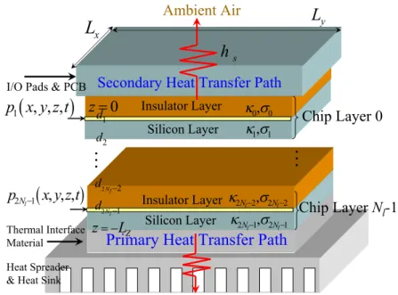
Thermal Model of 3D IC
Fig. 3.2 is the schematic representation of 3D integration, and Fig. 3.3 is its compact thermal model. As shown in Fig. 3.3, the structure of 3D IC is a multi-layer structure with stacking silicon and insulator layers one by one [22, 29]. This model consists of three portions [92]: the primary heat flow path, the secondary heat flow path, and the heat transfer characteristic of each macro/block on the silicon die. The primary heat flow path is composed of thermal interface material, heat spreader and heat sink. The secondary heat flow path contains I/O pads and the print circuit board (PCB). The functional blocks are modeled as many power generating sources distributed in a thin layer close to the top surface of each active silicon layer in the z-direction, and each insulator layer consists of Cu, ILD and glue materials.
3.2.2
First Stage
In the first stage, given an initial temperature, we substitute it into (2.10) and multiply the
leakage currents shown in (2.8) and (2.10) with supply voltages to get the leakage power Psub=
VDDIsuband Pgate= VDDIgate. Then, we build the projected leakage power cell library for each
type of gate in every KL grid of each layer, and we use the 1-D thermal model and the mean of the power to set the thermal parameters and do the thermal simulation. After getting the
new temperature, we rebuild the subthershold leakage power cell library by the average mean temperature. Note that the gate leakage power is temperature independent so we only calculate it once in the whole flow. The above steps are performed iteratively until the average mean temperature converges; thus we get a more accurate initial temperature.
3.2.3
Second Stage
In the second stage, we first compute the power with the more accurate initial temperature got in the first stage and obtain the mean temperature by using an efficient 3D deterministic GIT thermal simulatior [91]. Then, we obtain the first order PC expansion of the multi-layer temperature distribution. T (r, $, θ) ' NKL X k=0 Tk(r)ξk, (3.1)
where each Tk(r) is the coefficient function of the temperature projection onto the k-th
H-PC, r is the position. The spatial mean and variance distributions of the full-chip temperature distribution can be obtained as
E{T (r, $, θ) + Ta} ≈ T0(r) + Ta, (3.2) V ar{T (r, $, θ) + Ta} ≈ NKL X k=1 Tk2(r)E{ξ2}. (3.3)
The temperature is treated as a random process and is substituted into (2.10) to rebuild the subthreshold leakage power cell library. Those new leakage values are used to analyze the temperature distribution on the chip statistically. The above steps are performed iteratively until the mean and variance of the temperature converge.
3.3
Temperature Aware Statistical Timing Analysis
In this work, our SSTA is based on the widely used block based algorithm [51]. The delay is expressed in the canonical first-order form below:
Delay = a0+ a1Lef f + a2tox+ a3T, (3.4)
where a0 is the nominal value, and ai’s which are VDD dependent are the sensitivities to the
Input: Fitted cell leakage power, Dynamic power, Placement, Spatial correlation function
Output: The spatial mean and variances for the full–chip temperature distribution
First stage
1. Parameter modeling by Karhunen–Loeve expansion 2. Build projected power cell library of each layer with
the given initial temperature
3. Use 1–D thermal model and average mean temperature to set the thermal parameter
4. Re–build the subthreshold leakage power library by average mean temperature
repeat steps 2∼4 until the mean temperature converges Second stage
1. Obtain mean temperature by using 3D deterministic GIT thermal simulator
2. Obtain the first order PC expansion of the multi–layer temperature distribution
3. Re–build the subthreshold leakage power library repeat steps 1∼3 until means and variances of temperature
Fig. 3.4: Algorithm of the statistical thermal simulation.
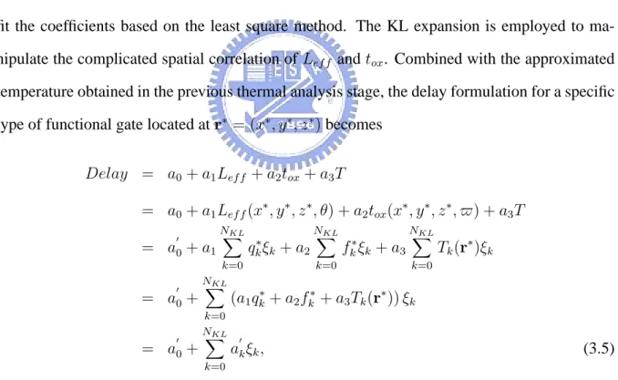
fit the coefficients based on the least square method. The KL expansion is employed to
ma-nipulate the complicated spatial correlation of Lef f and tox. Combined with the approximated
temperature obtained in the previous thermal analysis stage, the delay formulation for a specific
type of functional gate located at r∗ = (x∗, y∗, z∗) becomes
Delay = a0 + a1Lef f + a2tox+ a3T = a0 + a1Lef f(x∗, y∗, z∗, θ) + a2tox(x∗, y∗, z∗, $) + a3T = a00 + a1 NKL X k=0 q∗kξk+ a2 NKL X k=0 fk∗ξk+ a3 NKL X k=0 Tk(r∗)ξk = a00 + NKL X k=0 (a1qk∗+ a2fk∗+ a3Tk(r∗)) ξk = a00 + NKL X k=0 a0kξk, (3.5) where qk∗ = √χmqm(x∗, y∗, z∗) and fk∗ = √ βnfn(x∗, y∗, z∗), respectively. Equation (3.5) is
consistent with the canonical first-order delay form in [51]. As a result, the thermal effect can be easily considered in the SSTA without any extra complexity.
After setting up the canonical form of the delay, we explain how to execute the SUM and
MAX operations in the statistical timing analysis. Before showing the computation of the MAX
X and Y, the tightness probability TX of X is the probability that it is larger than (or dominates)
Y. The tightness probability TY of Y is (1-TX). Below we show how to compute the maximum
of two timing quantities in the canonical first-order form and how to determine their tightness probabilities. Given two timing quantities
A = a0+ n X i=i ai∆Xi, (3.6) B = b0+ n X i=i bi∆Xi, (3.7)
and the definitions
φ(x) = √1 2πexp(− x2 2 ), (3.8) Φ(y) = Z y −∞φ(x)dx, (3.9) θ = (σA2 + σB2 − 2ρσAσB)1/2, (3.10)
where ρ is the correlation coefficient, σA and σB are the standard deviation of A and B
respec-tively, the probability that A is larger than B is
TA = Z ∞ −∞ 1 σA φ(x − a0 σA )Φ(( x−b0 σB ) − ρ( x−a0 σA ) √ 1 − ρ2 )dx = Φ(a0− b0 θ ), (3.11)
The mean and variance of MAX(A,B) can also be analytically expressed as
E{M AX(A, B)} = a0TA+ b0(1 − TA) + θφ( a0− b0 θ ), (3.12) V ar{M AX(A, B)} = (σA2 + a20)TA+ (σB2 + b 2 0)(1 − TA) (3.13) +(a0+ b0)θφ( a0− b0 θ ) − (E{M AX(A, B)}) 2 , (3.14)
Hence we get the mean and variance of C=MAX(A,B). Mathematically,
ci = TAai+ (1 − TA)bi, (3.15)
where TAis the tightness probability of A. The maximum of two Gaussians is not a Gaussian but
we re-express it in the canonical Gaussian form so we can propagate the delay in the analysis. The method proposed in [60] is used to reduce the error induced by this approximation.
On the other hand, when a new timing quantity C is the summation of A and B, it is computed as follows C = A + B = c0+ n X i=i ci∆Xi = (a0+ b0) + n X i=i (ai+ bi)∆Xi (3.16)
3.4
Voltage Island Generation in 3D ICs
A significant concept of three dimensional voltage island generation is that we have to consider all the tiers at the same time instead of considering each tier sequentially. An obvious reason is that the timing budget is limited. If we perform the voltage island generation tier by tier, the available timing budget will become less and less. This will result in an ill circuit which its power consumption distribution on the chip is extremely unbalanced. On the other hand, the structure of the 3D IC is different with the 2D IC because of the vertical counterpart. For example, the power consumption may be acceptable for a region in a specific tier, but its upper or lower counterpart has high power consumption, which causes the thermal problem in the vertical space. If the upper or lower counterpart can not operate at the low supply voltage, we can do the power saving in the central region.
3.4.1
Voltage Assignment
In the beginning, the timing budget of the circuit is checked to guarantee that the power re-duction is available. The program stops the execution when the timing budget is not sufficient; otherwise, the assignment procedure is performed. After the verification, each tier is partitioned
into many grids, and the sensitivity of each grid i (gridi) is defined as the summation of each
gate’s sensitivity in gridi.
Sengridi =
X
gatej∈gridi
Sengatej. (3.17)
The number of sites in each grid is also recorded.
The next step is to vertically compress the three dimensional structure into a two dimen-sional planar, and several criteria are accumulated for each compressed grid. According to the
importance, these criteria include: 1) the power-delay sensitivity, 2) the power density induced weights and 3) the total number of sites.
The power-delay sensitivity is the most important criterion since the power dissipation re-duction is the primary target. A low (high) supply voltage reduces (increases) the power con-sumption but slows (accelerates) the speed of the gate. To utilize the timing budget effectively and achieve the most power saving, the power-delay sensitivity metric [93] is used as our opti-mization criterion. For each gate i, the power-delay sensitivity [93] is
Sengatei =
( ∆P
i
∆DiSlacki, Slacki ≥ ∆Di;
0, else; (3.18)
where Slackiis the timing slack of gate i, ∆Piand ∆Diare the power dissipation difference and
the delay difference for providing the low supply voltage for gate i instead of the high supply voltage, respectively. The gate which does not have enough slack for using the low supply voltage is called a site. For the purpose of the statistical power-delay sensitivity computation,
each ∆Di is fitted by the least square method as the first-order form with respect to Lef f, tox
and T which is similar to equation (3.4), and each ∆Piis fitted by the least square method as the
exponential form with respect to Lef f, toxand T which is similar to equations (2.8) and (2.10).
With equations (2.4)(2.5)(3.1) and a similar derivation to equation (3.5), for each gate i, the
expressions of ∆Piand ∆Di are
∆Pi= ∆Pdynamici+ ∆Psubi + ∆Pgatei
= pi0 + c 0 i0exp NKL X k=1 c0i kξk + b 0 i0exp NKL X k=1 b0i kξk (3.19) ∆Di= di0 + NKL X k=1 dikξk. (3.20)
After executing our thermal aware SSTA, Slackican also be obtained as the following canonical
first-order form Slacki = si0 + NKL X k=1 sikξk. (3.21)
With the definition of the power-delay sensitivity metric in equation (3.18), the following
sta-tistical power-delay sensitivity metric is applied in our power reduction flow and Sengatei is
re-deifined as
Sengatei =
(
E{∆Pi}
E{∆Di} × E{Slacki} , probi ≥ η;
High
TT
em
pp
era
tture
(a)
(b)
(c)
Low
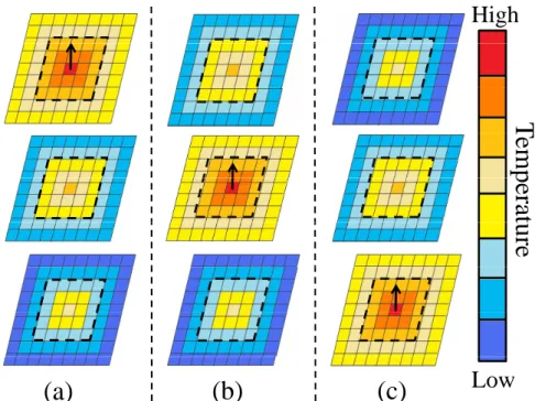
Fig. 3.5: A three-tier chip example for constructing the experimental model of power density induced weights. (a) An 1W power is inserted into the grid (5, 5) on the tier 1 and the corre-sponding temperature profile on each tier. (b) An 1W power is inserted into the grid (5, 5) on the tier 2 and the corresponding temperature profile on each tier. (c) An 1W power is inserted into the grid (5, 5) on the tier 3 and the corresponding temperature profile on each tier. The color bar shows the related levels of the temperature with respect to the colors on tiers. The ar-rows indicate the 1W power sources. The rectangles with dotted line margins are the truncation regions.
Here, probi = prob (Slacki≥∆Di), which is the tightness probability of Slacki and can be
obtained in constant time by performing table look-up, and η is a user-specified threshold value. The second important criterion is the power density induced weights among the compressed grids because the hot-spot issue must be avoided during executing our power reduction method. The power density induced weights of grids are obtained as follows. First, we make an ex-perimental model for the power density induced weights. As shown in Fig. 3.5, an 1W power source is orederly inserted to the central gird of each tier and its correponding temperature pro-files of tiers are obtained. The above step is to approximate the spatial impulse response of the heat transfer equation for a specified 3D IC. Then, these correponding temperature profiles are normalized in the range from 0 to 1 by using the maximum temperature among all of these cor-reponding temperature profiles. Finally, the truncation regions of these normalized temperature profiles are obtained by a specified threshold value.
spatial impulse responses for the heat transfer equation only depends on the package structure, chip dimension and the thermal parameters of a specified 3D circuit. Therefore, it can be re-used during our power reduction method being executed. Although the spatial impulse responses of the heat transfer equation for a specified 3D circuit are various in different locations, the weights in the truncation regions of grids are slightly different in our experimental results. For the efficiency, all of grids are set to share the same weights in their truncation regions in our
implementation1. With these truncation regions, the power density induced weight of grid j
induced by grid i can be obtained as the product of the power density of grid i with the weight of the truncation regions which corresponds to grid j. Consequently, the accumulated value of each grid is the summation of the power density induced weights from itself and from the neighboring grids among tiers.
Here, power density of grid i is obtained by using µPTi+ 3σPTi to ensure the thermal safety.
PTi is the power consumption in grid i. µPTi and σPTi can be computed by using the means
and variances of powers of various types of gates in grid i. For a specific type of gate in grid i, mean and variance of the power can be obtained by substituting equations (2.4)(2.5)(3.1) into equations (2.8)(2.10) and then obtain the means and variances of equations (2.8)(2.10). For example, after substituting equations (2.5)(3.1) into equation (2.10), we obtain the following computational formulas for mean and variance of the subthreshold leakage power for a type of gate in grid i.
E{Psub} = ˆc0exp
1 2 NKL X k=1 βk2 , (3.23)
V ar{Psub} = ˆc20exp
NKL X k=1 βk2 , (3.24)
where ˆc0 and each βkare known values consisted of supply voltage and the leading coefficients
of ξkof Lef f and T (r, θ, ω) in equations (2.5)(3.1).
The gate called site will violate the timing constraint when it is assigned with the low supply voltage so we must avoid generating too many sites during the proposed assigning procedure. In fact, this criterion is related to the power-delay sensitivity criterion because the site contributes zero sensitivity, and the grid with the high sensitivity should not contain too many sites.
1If a more accurate result is required, truncation regions with different weights can be obtained for the grids in
Fig. 3.6: A three-tier design example of the grid-based procedure for generating the voltage islands. Each tier is first divided into many grids, and the grid with the high sensitivity has dark color. After compressing, the criteria are accumulated, the higher priority the grid has, the darker the color is. When the grid with the highest priority is found, it is restored to the multi-layer structure to decide which tier should operate at the low supply voltage.
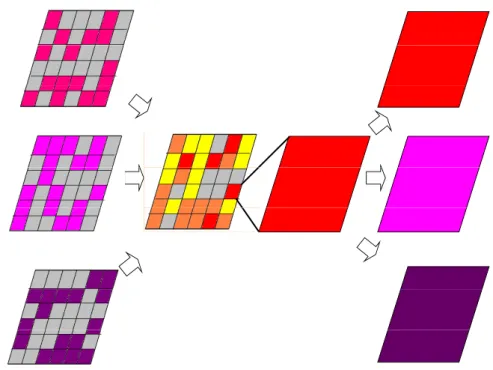
After compressing, the priority of each compressed grid is decided by these three criteria, and the grid with the highest priority is selected. Then, the selected compressed grid is restored back to the multi-layer structure. This procedure is helpful for us to understand whether the accumulated sensitivity is contributed by a grid on a specific layer or by all the grids on every layer averagely and to decide the grid for using the low supply voltage. Finally, every gate in this grid is assigned with the low supply voltage. When there are more than two supply voltages, the designer can decide to lower the supply voltage to next level or to the smallest level. A three-tier design example of the above grid-based procedure for the voltage assignment is illustrated in Fig. 3.6.
3.4.2
Incremental Update
When a grid is assigned with the low supply voltage, the timing and power-delay sensitivity information of many gates are affected and should be updated. To get the exact slack and sensi-tivity information in the circuit, performing the SSTA after every low supply voltage assignment is an instinctive but costly idea. For reducing the computational load, we use an incremental
approach to approximately update the sensitivity. The basic idea is borrowed from the STA. For example, the gate C in Fig. 3.7 has two input signals which are from the outputs of gate A and gate B. The AT of gate A and gate B are 2 and 5 by using the STA, respectively; the AT of C is determined by the latest arriving input B. If gate A is decided to operate at the low supply voltage and the AT of A increases to be 4 now, C is not affected because B is still the slowest input. Nevertheless, if the AT of A becomes 6, the AT of gate C is changed and the increment is 1. To conclude, the low supply voltage assignment will impact C only when the new AT exceeds the dominated one.
This similar concept can be used in the statistical manner by replacing the deterministic delay by the random variable delay and using the available mathematical method to do compar-ison between two random variables in probabilistic forms. In this example, the gate C records its latest arriving input M = M AX(A, B) as shown in Fig. 3.7(d) after the initial timing
analy-sis. When the low supply voltage is assigned to gate A, the AT of A is changed to A0. Then,
we compare these two random variables. If prob(A0 ≥ M ) ≥ α, where α is a user-defined
bonding parameter, it means that gate C is heavily affected by this assignment. Therefore, the
new latest arriving input becomes to M0 = M AX(A0, M ) and the arrival time of C is updated.
Similarly, the required time of gate can be updated by the smallest one. After the update of AT and RT, the slack and power-delay sensitivity information of gate are updated.
3.4.3
Site Rescue
The next issue is about the sites in the circuit. Although the grid with sites is not assigned with low supply voltage, timing violations may still happen because we reduce the supply voltage for the gates in one grid at the same time and update the timing approximately. In the timing-check stage, if any gate violates the timing constraint, the program will use several ways to recover the timing. The first method is the placement refinement. Since the site can not operate at the low supply voltage, we try to find a replacer, which is a gate with the largest sensitivity in the neighboring grids operating at the high supply voltage, to exchange its location with the site as shown in Fig. 3.4.5(a). If a replacer is not available, the site will be pushed to a neighboring grid operating at the high supply voltage as illustrated in Fig. 3.4.5(b). The second method is the gate-sizing. According to the cell library, the program selects a size for the site to satisfy
AT = 2 AT = 5 Max(A,B)=5 AT = 4 AT = 5 Max(A,B)=5 AT = 5 AT = 6 Max(A,B)=6 (a) (b) (c) (d) Max(A,B)=
Fig. 3.7: (a) Initial state. (b) The low supply voltage is assigned to gate A, but the AT of gate C is not affected. (c) The low supply voltage is assigned to gate A, and the AT of gate C is affected. (d) Statistical form.
(a) (b)
Fig. 3.8: The grids with dark color operate at low supply voltage and the grids with light colors operate at high supply voltage. The red block is the site and the blue block is the replacer. the timing constraint with less power dissipation. Although sizing up the gate size will increase a little power consumption, it is worth because of the large power saving from other gates in the grids. Lastly, if these techniques fail to recover the timing, the design will return to the last timing-satisfied condition with the least power dissipation.
3.4.4
Post Tuning
The proposed voltage assignment and incremental update approach are very efficient in run-time. The avoidance of timing violations and the grid-based structure nevertheless limit the assignment to the grid without any site and sacrifice some gates that have potential power sav-ing. Hence, we provide a slower but finer gate-based post tuning step to further improve the assignment result. This gate-based procedure uses the same statistical power-delay sensitivity as guidance. Once the gate with highest sensitivity is found, it is assigned to low supply voltage for power reduction. Through a SSTA run, the action is accepted unless the timing constraint is violated. This process repeats until no further power reduction can be made.
3.4.5
Grouping and Extension
After the voltage assignment and post tuning, methods proposed in [72, 74] can be utilized to complete the voltage island generation. Based on their idea, there are still several improvements which can be exploited. Fig. 3.9 illustrates this idea. In this figure, red color means the highest supply voltage, and dark blue and light blue represent the middle and the least supply voltage, respectively. Fig. 3.9(a) is the result of voltage assignment. Fig. 3.9(b) is the result of process in [72]. A dark blue grid is annexed to the red grids to reduce the number of islands. Since the timing resource belonged to the dark blue grid is released due to this mergence, the island with lower supply voltage can extend its range. When there are more than two supply voltages, the timing resource can be utilized by any supply voltage except the highest one. In this example, for the least voltage, the yellow grids are the possible regions for the extension as shown in Fig. 3.9(c). Fig. 3.9(d) is the result of the island extension, so the power consumption is further reduced.
Initially, every grid with low supply voltage is viewed as an single island. The proposed method first scans the topology and groups the single islands that are adjacent to each other into big islands. The action results many base islands which may be composed of only one grid or several grids and each base island has a size which is equal to the number of grids it contains. Second, some base islands are deleted when their size is smaller than an user-specified size bound. This is similar to [72] since these small islands can consume many power network
(a)
(b)
(c)
(d)
Fig. 3.9: Voltage Island Extension
resource and they would be merged like Fig. 3.9(a)(b). The process next finds the neighbors, which are the grids next to the base islands. Then, these base islands start to extend their region to the neighbors with the resource from the deletion as shown in Fig. 3.9(c)(d). The power-delay sensitivity is still used as guidance and the extension is allowed when there is no timing violation. Eventually, the voltage islands are generated.
Chapter 4
Experimental Results
The proposed approach has been implemented in C++, and been applied to a set of ISCAS89 benchmark circuits and private designs. The benchmark circuits are synthesized by using De-sign Compiler with the UMC 90 nm standard cell library. After that, the SOC Encounter is used to generate an initial 2D placement. Then we transform the 2D placement to a 3D placement with Z–Place provided by professor Renato [94]. The ranges of the process variations (3σ) are:
Lef f: 20 %, tox: 20 %. The Karhunen–Loeve transformation is employed to deal with the
phys-ical parameters with spatial correlation. The number of reference points is set to be 16 for the parameter modeling of the channel length and the oxide thickness. For the delay constraints, we consider the timing yield target of 99 %. The timing/leakage power cell library with process variations is generated as follows. We evaluate the average leakage current and gate delay based on H-SPICE simulation for various types of logic gates. From the H-SPICE simulation results, we obtain the fitting constants of the leakage current and gate delay models based on the least square method.
2 2.5 3 3.5 4 4.5 5 0 0.5 1 1.5 2 2.5 3 3.5 t = 2 to 5 (ns) P ro b ab il it y D en si ty
Temperature Impact on Slack Distribution
Slack with thermal simulation Slack with nomial temperature
Fig. 4.1: Temperature impact on slack distribution.
• Thermal Aware SSTA
Our first comparison gives the impact of temperature on delay computation. Fig. 4.1 shows the slack distribution both with the statistical 3D thermal simulation result and the nominal temperature in [19]. As observed in this figure, for the slack distribution, the mean will decrease and the variance will increase when statistical thermal simulation is utilized. Since thermal problem is one of the critical challenges in 3D IC design, considering the temperature impact in circuit analysis is an essential work.
Table 4.1: Leakage Power Estimation
With Statistical Temperature With Nomial Temperature Difference(%)
Circuit Leakage Power (µW ) Total Power (µW ) Leakage Power (µW ) Total Power (µW ) Leakage Power Total Power
s1488 46.15 560.03 31.51 555.64 31.71 0.78 s1494 46.47 564.10 31.93 559.74 31.30 0.77 s5378 1144.90 2190.06 104.71 1878.00 90.85 14.25 s9234 1 490.82 1514.86 99.35 1397.42 79.76 7.75 s13207 1180.84 2461.10 185.81 2162.59 84.26 12.13 s35932 3381.22 6682.40 1122.90 6004.90 66.79 10.14 s38417 5025.33 10312.62 904.73 9076.44 82.00 11.99 s38584 3257.71 7149.88 847.62 6426.85 73.98 10.11 Circuit 1 1701.47 5281.69 1217.42 5136.48 28.45 2.75 Circuit 2 5884.27 9204.04 5161.80 8987.30 12.28 2.35 Circuit 3 3516.46 6085.30 2875.25 5892.94 18.23 3.16 Avg. 54.51 6.93
• Temperature Impact ono Leakage Power Estimation
Table 4.1 lists the leakage power and total power estimation with the simulated temper-ature (columns 2, 3) and the nominal tempertemper-ature in [19] (columns 4, 5), the percentage differences of leakage power, and total power (columns 6, 7), respectively. Here, we sup-pose the ratio of the leakage power to the total power is 30 % [16]. As show in this table, the full chip leakage power analysis without accurate temperature can lead to 54 % error in average. When the leakage power is underestimated, the optimization work would be dominated by the dynamic power, which may result a non-ideal design.
![Fig. 1.1: Leakage variations [18]](https://thumb-ap.123doks.com/thumbv2/9libinfo/8653577.194194/11.892.223.713.419.705/fig-leakage-variations.webp)
![Fig. 2.1: Assembly process for a 3D chip [38]](https://thumb-ap.123doks.com/thumbv2/9libinfo/8653577.194194/15.892.163.780.527.1092/fig-assembly-process-d-chip.webp)