Power-Efficient FIR Filter Architecture Design for
Wireless Embedded System
Shyh-Feng Lin, Student Member, IEEE, Sheng-Chieh Huang, Feng-Sung Yang, Chung-Wei Ku, and
Liang-Gee Chen, Fellow, IEEE
Abstract—This paper presents a novel approach for imple-menting power-efficient finite-impulse response (FIR) filters that requires less power consumption than traditional FIR filter implementation in wireless embedded systems. The proposed schemes can be adopted in the direct form FIR filter and achieve a large amount of reduction in the power consumption. By using a combination of proposed methods, balanced-modular techniques with retiming and separated processing data-flow scheme with modified canonical signed digit (CSD) representation, experi-mental results show that the proposed scheme reduce 76% power consumption of the original direct-form structure with slight area overhead.
Index Terms—Canonical signed digit (CSD), direct form, em-bedded, finite-impulse response (FIR), power-efficient, retiming, wireless.
I. INTRODUCTION
I
N SEVERAL wireless hand-held systems, the finite-impulse response (FIR) filters are the indispensable parts among var-ious image/video communication applications to reduce noise and to enhance the specific features. With a given specification, the dedicated filter is designed to fit in the applications and has the least effect of redundancy.However, the previous designs of the dedicated filter archi-tecture still have some drawbacks. The overhead of the subex-pression sharing [1], [2] is a complicated routine like a chaotic adder tree. To keep timing correct, the substructure sharing will make the registers grow rapidly. Therefore, this approach is dif-ficult for the hardware implementation. In addition, the advan-tage of the fixed coefficients can not be utilized by the folded architecture [3], [4]. Hence, the folded architecture loses the benefit in the chip area and the power consumption. The di-rect form and the transposed form [5], [6] usually represent the filter coefficients in the canonical signed digit from (CSD) to decrease the nonzero digits of the constant multipliers. At the same time, Firgen [5] and Laskowski [6] contributed to the elim-ination of the MSB sign-extension redundancy. However, the Manuscript received February 20, 2002; revised July 11, 2003. This paper was recommended by K. Parhi.
S.-F. Lin, S.-C. Huang, and L. G. Chen, are with the Department of Electrical Engineering, Graduate Institute of Electronics Engineering, R344, National Taiwan University, Taipei 106, Taiwan, R.O.C. (e-mail: lgchen@ video.ee.ntu.edu.tw).
F.-S. Yang is with the IC Design Group, 8TECH, Inc., Taipei 106, Taiwan, R.O.C.
C.-W. Ku is with the DSP Group, VIVOTEK Inc., Taipei 106, Taiwan, R.O.C. Digital Object Identifier 10.1109/TCSII.2003.821513
Fig. 1. Retimed direct form architecture.
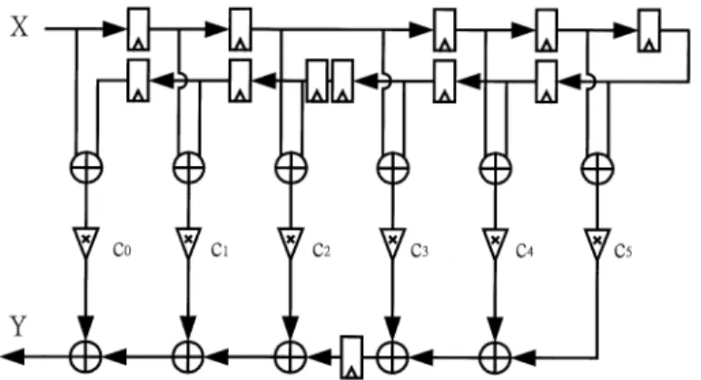
Fig. 2. Symmetrical Retimed linear-phase direct form architecture with 12 taps.
disadvantage is that the structural symmetry in the linear-phase frequency response can not be applied to transposed form filters designs.
In this paper, we provide a solution to the problems de-scribed above by designing an FIR filter based on the archi-tecture with modular design. The routing scheme is not very complicated and it still keeps the symmetric, and multiplier-less benefits. Besides, adding the proposed separated sign pro-cessing with modified CSD representation will have excellent results both in balancing critical-path delay and suppressing circuit transition.
II. PROPOSEDARCHITECTURE
In this paper, the direct form of dedicated FIR with CSD co-efficient representation is considered. There are four steps to re-duce the power consumption.
A. Symmetrical Retimed Direct Form Architecture
Retiming method can decrease the critical path as the pipeline method but without increasing the latency of circuit. If the phase of the filter is linear, the symmetrical architecture 1057-7130/04$20.00 © 2004 IEEE
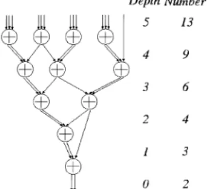
Fig. 3. Example of carry-save adder tree.
Fig. 4. Summation of partial products.
can be used to reduce the multiplier operation. Comparing Figs. 1 and 2, the number of multipliers can be reduced half after adopting the symmetrical architecture. The symmetrical retimed direct form architecture (RDFA) takes the advantage in speed and area, and it is the basic model to develop the proposed architecture.
B. Balanced Modular Architecture (BMA)
The same nonzero digits instead of the same numbers of co-efficients are chosen, because the multiplier in each stage is not identical to each other. And a carry-save adder tree adopted with the same depth is used in the modular design. Since the Wallace tree uses the 3:2 compression ratio, the bit numbers of each bit plane are 9, 6, 4, 3, and 2 in the Wallace tree as shown in Fig. 3. An example to explain this situation is illustrated in Fig. 4, where the formula
contains 9 nonzero coefficients digits. The maximal number of summation of par-tial products is 9, and the corresponding depth of the carry-save adder tree is 4. After considering these ideas, the resulted filter structure is displayed in Fig. 5.
C. Separated Signed Processing Architecture
The 2’s complemented number representation for VLSI design will cause amounts of power consumption while the
each sign are finally utilized, stored, and merged together. In order to avoid the transition between positive and negative caused by the input data, the filter input must be biased to a positive number instead of the sign-magnitude representation. These biases at the last stage of the accumulating path are deleted. As a result in Fig. 6, this design processes the biased input signal X in two different datapaths for each sign without any control. Eventually, the results positive part and negative part from the datapaths and the compensation bias are summed together to get the final result.
D. Modification to the CSD (MCSD) Representation
Separated signed processing will produce the unbalanced module. Although, the occurrences of positive and negative digits have the same probability, it is just the average statistics. The modification of the CSD representation is proposed to solve the problem. The concept is to modify the CSD repre-sentation to balance the positive and negative parts, and the number of nonzero digits is the same as before. For example, if the number of positive digits is much less than that of negative digits, then should be changed into 011 to increase the number of positive digits while decreasing the number of negative digits. Evidently the modified CSD coefficients result in a structure shown in Fig. 7 has higher utilization of hardware than the one in Fig. 6.
III. COMPARISONS ANDDISCUSSIONS
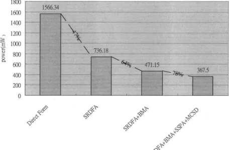
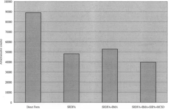
This section shows an example for IS-95 WCDMA pulse shaping FIR filter. The ideal floating-point coefficients of an IS-95 WCDMA FIR filter with 33-taps for the third-genera-tion cellular phone. From our power analysis the symmetrical retimed direct form architecture (SRDFA) just needs 47% power consumption compare with the original direct-form ar-chitecture. Applying BMA will reduce to 64% of original power. By combining SSPA with MCSD representation, the power consumption can be reduced to 78% of the original one. If the four schemes are adopted together, the power consumption can decrease to 24% original direct-form archi-tecture. The simulation results are shown in Table I, Figs. 8 and 9.
Compared to the linear-phase direct form architecture for IS-95 WCDMA filters, the modularization obviously decreases the transition count as shown in Table II. When the FIR filter is fed with a sequence of randomly generated data, the result is similar. For the IS-95 WCDMA pulse shaping filter, adopting the proposed architecture can reduce the number of circuit transition to be 71.4%.
Fig. 5. Balanced modular FIR filter architecture.
Fig. 6. Architecture with 4-level pipeline of pulse-shaping filter for IS-95 WCDMA.
Fig. 7. The 3-level pipeline architecture of pulse-shaping filter for IS-95 WCDMA after adopting MCSD.
Fig. 9. Area comparison of the proposed four schemes.
TABLE I
COMPARISONRESULTS OF THEPROPOSEDFOURSCHEMES
TABLE II
THENUMBER OFCIRCUITTRANSITIONS OFTHREECASES
IV. CONCLUSION
In this paper, a low-power architecture for dedicated linear phase FIR filter is proposed. Four schemes are suggested, including retimed structure, balanced modular architecture, separated signed processing data flow and modification of the CSD representation. From the experimental results, the proposed signal processing schemes reduce about ten to 30% circuits’ transition in the accumulation path to achieve the maximum efficiency of hardware components. The proposed schemes not only address the linear-phase FIR filter, but also can improve the non linear-phase FIR filer.
REFERENCES
[1] G. Wacey and D. R. Bull, “POFGEN: A design automation system for VLSI digital filters with invariant transfer function,” in Proc. IEEE Int. Symp. Circuits and Systems (ISCAS), vol. 1, 1993, pp. 631–634. [2] M. Abo-Zahhad and S. M. Ahmed, “Filter designer: A complete design
and synthesis program for lumped, wave-digital, FIR and IIR filters,” in Proc. 13th National Radio Science Conf., Cairo, Egypt, Mar. 9–21, 1996, pp. C24.1–C24.15.
[3] V. Verma and C. Chien, “A VHDL based functional compiler for op-timum architecture generation of FIR filters,” in Proc. IEEE Int. Symp. Circuits and Systems (ISCAS), vol. 4, 1996, pp. 564–567.
[4] W. Wilhelm and T. G. Noll, “A new mapping technique for automated design of highly efficient multiplexed FIR digital filters,” Proc. IEEE Int. Symp. Circuits and Systems, (ISCAS), vol. 4, pp. 2252–2255, 1997.
[5] R. Jain, P. T. Yang, and T. Yoshino, “FIRGEN: A computer-aided design system for high performance FIR filter integrated circuits,” IEEE Trans. Signal Processing, vol. 39, pp. 1655–1668, July 1991.
[6] J. Laskowski and H. Samueli, “A 150-MHz 43-tap half-band FIR digital filter in 1.2-um CMOS generated by silicon compiler,” in Proc. Custom Integrated Circuits Conf., 1992, pp. 11.4.1–11.4.4.
[7] T. Yamazaki, Y. Kondo, S. Igota, and S. Iwase, ““FASTOOL” an FIR filter compiler based on the automatic design of the multi-input-adder,” in Proc. IEICE Trans. Fund., vol. E78-A, Dec. 1995, pp. 1699–1705. [8] R. I. Hartley, “Subexpression sharing in filters using canonic signed digit
multipliers,” IEEE Trans. Circuits Syst. II, vol. 43, pp. 677–688, Oct. 1996.
[9] R. Pasko, P. Schaumont, V. Derudder, and D. Durackova, “Optimization method for broadband modem FIR filter design using common subex-pression elimination,” in Proc. Int. Symp. System Synthesis, 1997, pp. 100–106.
[10] S. Sugawa, H. Shimamoto, S. Hosotani, Y. Imamura, T. Takagaki, H. Ijiri, K. Okada, and T. Sumi, “An area efficient hardware sharing filter generator for integration of multiple video format conversions,” in IEEE Int. Conf. Consumer Electronics Tech. Dig. Papers, 1997, pp. 414–415. 47 386.
[11] M. Potkonjak, M. B. Srivastava, and A. P. Chandrakasan, “Multiple con-stant multiplications: Efficient and versatile framework and algorithms for exploring common subexpression elimination,” IEEE Trans. Com-puter-Aided Design, vol. 16, pp. 151–165, Feb. 1996.
[12] M. Potkonjak, M. B. Srivastava, and A. Chandrakasan, “Efficient substi-tution of multiple constant multiplications by shifts and additions using iterative pairwise matching,” in Proc. 31st ACM/IEEE Design Automa-tion Conf., 1994, pp. 189–194.
[13] S. F. Lin, S. C. Huang, F. S. Yang, C. W. Ku, and L. G. Chen, “An effi-cient linear-phase FIR filter architecture design for wireless embedded system,” in Proc. IEEE Workshop Signal Processing System (SiPS), Antwerp, Belgium, Sept. 2001.
[14] K. Azadet and C. J. Nicol, “Low-power equalizer architectures high-speed modems,” IEEE Commun. Mag., vol. 36, pp. 118–126, Oct. 1998.