四閘極金氧半場效電晶體之具氧化層基體絕緣結構(含/不含)氧化層介面缺陷電荷之次臨界行為研究
194
0
0
全文
(2) 四閘極金氧半場效電晶體之具氧化層基體絕緣結構(含/不 含)氧化層介面缺陷電荷之次臨界行為研究 指導教授:江德光 博士 國立高雄大學電機工程系 電機工程研究所 學生:高鴻文 國立高雄大學電機工程系 電機工程研究所 摘要 過去數十年來,有許多關於平面單閘極電晶體與雙閘極電晶體之熱載子效應引起的 次臨界行為研究,熱載子效應所引起的氧化層缺陷介面電荷,造成臨界電壓漂移及元件 的電子參數特性的改變。截至目前為止,含氧化層缺陷介面電荷之四閘極電晶體的次臨 界電特性的研究仍相當欠缺,而針對植入帶電電荷改變電特性之記憶體元件(Charge Trapped or Injection Memory Device)應用而言,實有必要研究其次臨界行為特性與表面 缺陷電荷之關係,以期該元件將來被有效應用於記憶體電路中,本論文乃基於帕森方程 式三維近似解與全三維解,成功地推導出含氧化層缺陷介面電荷之四閘極電晶體具氧化 層基體絕緣結構之次臨界行為解析模型。 本論文乃基於帕森方程式、微縮理論及周長加權近似法,成功地推導出四閘極電晶 體具氧化層基體絕緣結構之次臨界行為解析模型,此模型不僅準確顯示出電位分佈 (potential distribution) 、 次 臨 界 斜 率 (subthreshold slope) 、 次 臨 界 電 流 (subthreshold current) 、 和 臨 界 電 壓 縮 減 (threshold voltage degradation) 、 汲 極 偏 壓 導 致 能 障 降 低 (drain-induced-barrier-lowering, DIBL)等效應,而且此模型與元件模擬數據相當接近,足 以提供基本元件設計之導向,並進而被應用於積體電路設計之模擬。. 關鍵字:四閘極金氧半場效電晶體、氧化層缺陷介面電荷、短通道行為、短通道臨界電 壓縮減 i.
(3) The Investigation on Subthreshold Behavior Model for the SOI Quadruple-Gate MOSFETs with/without the Localized Interface Trapped Charges Advisor: Dr. Te-Kuang Chiang Department of Electrical Engineering, Institute of Electrical Engineering, National University of Kaohsiung Student: Hong-Wun Gau Department of Electrical Engineering, Institute of Electrical Engineering, National University of Kaohsiung ABSTRACT Several studies have modeled the hot-carrier-induced threshold voltage of the planar and the double-gate MOSFETs in the past decade. The hot-carrier-induced positive or negative charges can be trapped in the interface between the gate oxide and the silicon film, which can further cause the shift of the threshold voltage and deteriorate the electrical characteristic parameters of the device. Until now, there is no literature to investigate the subthreshold behavior model of the Quadruple-Gate (QG) MOSFETs with the localized interface trapped charges. With the application for Charge Trapped or Injection Memory Device, we report the Quasi 3-D/Fully 3-D analytical model of the subthreshold behavior for the Quadruple-gate MOSFETs. In this thesis, based on the exact solution of the Poisson equation,scaling theory and perimeter- weighted-sum approach, an analytical subthreshold model for the Quadruple-gate MOSFETs with localized interface trapped charges is developed by considering the effects of equivalent oxide charges on the flat-band voltage. The model explicitly shows the potential distribution, subthreshold slope, subthreshold current, threshold voltage, and drain-induced-barrier-lowing (DIBL) effect. The model is verified by the device simulator ”DESSIS”,and can be efficiently used to investigate the hot-carrier-induced threshold voltage degradation of the advanced QG MOSFETs charge-trapped memory device. This model not only gives the physical insights into the device physics but also offers the basic designing guidance of the SOI QG transistor. Due to its computational efficiency, this model can be applied for SPICE simulation. Keywords : Quadruple-Gate MOSFETs, Localized Interface Trapped Charges, Short-Channel Effect, Threshold Voltage Degradation ii.
(4) Acknowledgements It’s not easy for me when I stepped into the field of device from the study of multiple-gate device. I want to thank all the people who helped me. First of all, I would like to express my sincere appreciation to my advisor, Te-Kuang Chiang, for his guidance, encouragement and continuous support through the course of this work. Also, he told me the attitude toward work and life. That is inspirational.. I would like to thank the members of Advanced Device Simulation Lab for their support these years. I am very grateful to C.W. Liu for the support and help. I would like to thank Tsung.Ying Tsou, Yi. Hung Chiu. Many detailed and in-depth discussions with them have invaluably developed the derivation of SOI Multi-Gate MOSFETs model and device simulations.. Finally, this work is dedicated to my dear parents for their love and encouragement. I will be happy to continue my study in the coming years.. iii.
(5) Contents 摘要. i. Abstract. ii. Acknowledgements. iii. Contents. iv. List of Figures. vii. Chapter 1 Introduction....................................................................................................1 1.1 . 1Motive of the Thesis ......................................................................................1 1.1 . 1Quadruple-Gate Device Overview.................................................................3 Chapter 2 Quasi-Two Dimensional Subthreshold Behavior Model for SOI Quadruple-Gate MOSFETs with/without Localized Trapped Charges 2.1. 5. Quasi-Two Dimensional Subthreshold Behavior Model for SOI Quadruple-Gate MOSFETs..........................................................................5. 2.1.1. Model Derivation .........................................................................................5. 2.1.2. Boundary Conditions Value Problem...........................................................8. 2.1.3. Scaling Length .............................................................................................8. 2.1.4. Minimum Central Potential........................................................................10. 2.1.5. Threshold Voltage Model...........................................................................11. 2.1.6. Subthreshold Current Model......................................................................14. 2.1.7. Subthreshold Slope Model.........................................................................19. 2.1.8. Results and Discussion ..............................................................................23. 2.2. Quasi-Two Dimensional Subthreshold Behavior Model for SOI Quadruple -Gate MOSFETs with Localized Trapped Charges..................24. 2.2.1. Introduction................................................................................................24. 2.2.2. Model Description .....................................................................................26. 2.2.3. Quasi-2-D Generalized Potential Model....................................................27. 2.2.4. Threshold Voltage Mode............................................................................33. 2.2.5. Subthreshold Current Model......................................................................39. 2.2.6.1 Results and Discussion ..............................................................................43 iv.
(6) Chapter 3 Two Dimensional Subthreshold Behavior Model for SOI Quadruple-Gate MOSFETs with/without Localized Trapped Charges 3.1.1. 44. Two Dimensional Subthreshold Behavior Model for SOI Double-Gate MOSFETs.............................................................................44. 3.1.1. Model Derivation .......................................................................................44. 3.1.2. 2-D Boundary Conditions Value Problem .................................................46. 3.1.3. 1-D Solution...............................................................................................47. 3.1.4. Scaling Length ...........................................................................................48. 3.1.5. Coefficients Solution .................................................................................50. 3.1.6. 2-D Generalized Potential Model ..............................................................52. 3.1.7. Minimum Central Potential........................................................................55. 3.1.8. Threshold Voltage Model...........................................................................57. 3.1.9. Subthreshold Slope Model.........................................................................62. 3.1.10. Subthreshold Current Model....................................................................65. 3.2. Two Dimensional Subthreshold Behavior Model for SOI Quadruple -Gate MOSFETs with Localized Trapped Charges..................68. 3.2.1. Model Derivation .......................................................................................68. 3.2.2. 3-D Generalized Potential Model ..............................................................70. 3.2.3. Potential Contour .......................................................................................74. 3.2.4. Minimum Central Potential........................................................................76. 3.2.5. Threshold Voltage Model...........................................................................77. 3.2.6. Subthreshold Current Model......................................................................80. 3.2.7. Subthreshold Slope Model.........................................................................83. 3.2.8. Results and Discussion ..............................................................................86. 3.3.1. Two Dimensional Subthreshold Behavior Model for SOI Quadruple -Gate MOSFETs with Localized Trapped Charges..................87. 3.3.1. Introduction................................................................................................87. 3.3.2. Model Description Introduction.................................................................89. 3.3.3. 2-D Generalized Potential Model ..............................................................90. 3.3.4. Threshold Voltage Model...........................................................................95. 3.3.5. Subthreshold Current Model....................................................................102. 3.3.6. Results and Discussion ............................................................................106. Chapter 4. Three Dimensional Subthreshold Behavior Model for SOI Quadruple -Gate v.
(7) MOSFETs with/without Localized Trapped Charges 4.1. 107. Three Dimensional Subthreshold Behavior Model for SOI Quadruple -Gate MOSFETs.....................................................................107. 4.1.1. Model Derivation .....................................................................................107. 4.1.2. 3-D Boundary Conditions Value Problem ...............................................110. 4.1.3. 1-D Solution.............................................................................................111. 4.1.4. 2-D Coefficients Solution ........................................................................112. 4.1.5. 3-D Laplace Equation Solution................................................................114. 4.1.6. 3-D Generalized Potential Model ............................................................118. 4.1.7. Minimum Channel Potential ....................................................................122. 4.1.8. Threshold Voltage Model.........................................................................124. 4.1.9. Subthreshold Slope Model.......................................................................129. 4.1.10 Subthreshold Current Model.....................................................................133 4.2. Three Dimensional Subthreshold Behavior Model for SOI Quadruple -Gate MOSFETs with Localized Trapped Charges................136. 4.2.1. Model Derivation .....................................................................................136. 4.2.2. 3-D Boundary Conditions Value Problem ...............................................140. 4.2.3. 1-D Solution.............................................................................................143. 4.2.4. 2-D Coefficients Solution ........................................................................145. 4.2.5. 3-D Laplace Equation Solution................................................................148. 4.2.6. 3-D Generalized Potential Model ............................................................154. 4.2.7. Minimum Channel Potential ....................................................................157. 4.2.8. Threshold Voltage Model.........................................................................159. 4.2.9. Subthreshold Current Model....................................................................169. 4.3. Results and Discussion ...........................................................................173. Chapter 5 Conclusions and Future Works ................................................................174 5.1. Conclusions.................................................................................................174. 5.2. Future Works...............................................................................................174. References......................................................................................................................175 Publication List. 179. VITA. 180. vi.
(8) List of Figures Fig.1.1 SOI MOSFET family tree..............................................................................................2 Fig.1.2 Schematic of Quadruple-Gate MOSFETs: (a) three-dimensional device structure, (b) with cut plane along x direction(c) with cut plane along y direction. The device can be equivalently composed of two-dimensional symmetrical double-gate (SDG) MOSFET with width of W as shown in (b) and symmetrical double-gate (SDG) MOSFET with width of H as shown in (c)................................................................................................................................3 Fig. 2.1.1 Schematic of Quadruple-Gate (QG) MOSFETs with cut plane along x-direction....5 Fig. 2.1.2 The “equivalent number of gates” (ENG), natural length, and improvement in the minimum channel length for the single-gate, double-gate, triple-gate, and quadruple-gate MOSFETs. (Calculating parameters: H=W =10.0 nm, tox= 1.0 nm). .......................................9 Fig. 2.1.3 Variation of minimum surface potential Φ min with gate bias Vgs for different channel lengths.........................................................................................................................10 Fig. 2.1.4 The dependence of threshold voltage roll-off ΔVth and DIBL on channel length L for various gate oxide thicknesses ...........................................................................................12 Fig. 2.1.5 The dependence of threshold voltage roll-off ΔVth,s and DIBL on channel length L for various silicon film widths .................................................................................................13 Fig.2.1.6 The dependence of threshold voltage roll-off ΔVth,s on channel length L for different channel heights and widths ......................................................................................................13 Fig.2.1.7 The minimum channel length versus channel height H with the gate oxide thickness as a parameter. The comparison between DG, TG, and QG devices is carried out to meet the criterion of DIBL ≦50mV .....................................................................................................14 Fig. 2.1.8 The subthreshold current versus the gate bias for the different gate oxide thicknesses. ..............................................................................................................................17 Fig. 2.1.9 The subthreshold current versus the gate bias for the different silicon heights. .....17 Fig. 2.1.10 The subthreshold current versus the gate bias for the different workfunction ......18 Fig. 2.1.11 Analytical solution of the subthreshold slope for QG MOSFETs compared with 2D numerical simulation results with the silicon film heights as a varied parameter .............21 Fig.2.1.12 Analytical solution of the subthreshold slope for QG MOSFETs compared with 2D numerical simulation results with the gate oxide thickness as a varied parameter..................21 Fig.2.1.13 Analytical solution of the subthreshold slope for QG MOSFETs compared with 2D. vii.
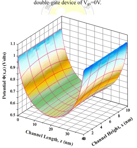
(9) numerical simulation results with the drain bias as a varied parameter ..................................22 Fig. 2.2.1 Schematic of quadruple-gate MOSFETs: (a) three-dimensional device structure. With cut plane x direction and y direction, the device can be equivalently composed of 2 two-dimensional symmetrical double-gate (SDG) MOSFETs with width of W as shown in (b) with width of H as shown in (c). The two-dimensional device structures of Fig. 2.2.1 (b) and Fig. 2.2.1 (c) are used to derive the model, where regions 1, 3, and 2 denote the fresh and damaged zones, respectively....................................................................................................26 Fig. 2.2.2 The dependence of channel potential on the normalized channel position for the different ratios of damaged zone to undamaged zone. ............................................................30 Fig. 2.2.3 The variation of the two-dimensional potential distribution with the channel length and channel height for the simulation (The blue plot is for the damaged device with the positive trapped charges, the green plot is for the fresh device, and the red plot is for the damaged device with the negative trapped charges)................................................................31 Fig. 2.2.4 The variation of the two-dimensional potential distribution with the channel length and channel height for the model results (The blue plot is for the damaged device with the positive trapped charges, the green plot is for the fresh device, and the red plot is for the damaged device with the negative trapped charges)................................................................32 Fig. 2.2.5 Threshold voltage degradation versus normalized damaged zone for different thicknesses of silicon body.......................................................................................................37 Fig. 2.2.6 Threshold voltage degradation versus normalized damaged zone for different thicknesses of gate oxide. ........................................................................................................37 Fig. 2.2.7 Threshold voltage roll-off versus gate length for both fresh and damaged devices. ..................................................................................................................................................38 Fig. 2.2.8 Threshold voltage degradation versus normalized damaged zone for DG, TG and QG MOSFETs.............................................................................................................38 Fig. 2.2.9 ITSUBD versus normalized damaged zone for different silicon body thicknesses 41 Fig. 2.2.10 ITSUBD versus normalized damaged zone for different gate oxide thicknesses .42 Fig. 2.2.11 SUBRUP versus gate length for the fresh and damaged devices ..........................38 Fig. 3.1.1 Schematic of QG MOSFETs with cut plane along x-direction. ..............................41 Fig. 3.1.2 The contour plot of the electrostatic scaling length versus insulator thickness and silicon thickness. ......................................................................................................................46 Fig. 3.1.3 The decay of Fourier series Dn, Pn, and Qn coefficients versus the term number ...51 Fig. 3.1.4 The 3-D potential distribution from the device simulator of DESSIS for viii.
(10) double-gate device of Vgs=0V. .................................................................................................53 Fig. 3.1.5 The 3-D potential distribution from the model results for double-gate device of Vgs=0V ...................................................................................................................................53 Fig. 3.1.6 The variation of the surface potential of Ф(x=0,z) and Ф(x=W,z) with the normalized channel length position of z/Lg for the different gate biases of Vgs=0V and Vgs=0.2V...................................................................................................................................54 Fig. 3.1.7 The variation of the channel potential Ф(x,z) with the normalized channel height position of x/W for the different channel locations of z=15nm, z=20nm, and z=25nm..........54 Fig. 3.1.8 Variation of minimum central potential Φ min with gate bias Vgs for different channel lengths.........................................................................................................................56 Fig. 3.1.9 The dependence of threshold voltage roll-off ΔVth,s on channel length L for various gate oxide thicknesses..............................................................................................................60 Fig. 3.1.10 The dependence of threshold voltage roll-off ΔVth,s on channel length L for various silicon film widths.......................................................................................................61 Fig. 3.1.11 The dependence of threshold voltage roll-off ΔVth,s on channel length L for various drain biases..................................................................................................................61 Fig.3.1.12 Analytical solution of the subthreshold slope for double-gate MOSFETs compared with 2D numerical simulation results with the silicon film widths as a varied parameter ......63 Fig. 3.1.13 Analytical solution of the subthreshold slope for double MOSFETs compared with 2D numerical simulation results with the gate oxide thickness as a varied parameter............64 Fig. 3.1.14 Analytical solution of the subthreshold slope for double-gate MOSFETs compared with 2D numerical simulation results with the drain bias as a varied parameter ....................64 Fig. 3.1.15 Analytical solution of the subthreshold current for double-gate MOSFETs compared with 2D numerical simulation results with the gate oxide thickness as a varied parameter..................................................................................................................................66 Fig. 3.1.16 Analytical solution of the subthreshold current for double-gate MOSFETs compared with 2D numerical simulation results with the channel width as a varied parameter. ..................................................................................................................................................67 Fig.3.1.17 Analytical solution of the subthreshold current for double-gate MOSFETs compared with 2D numerical simulation results with the channel length as a varied parameter. ..................................................................................................................................................67 Fig. 3.2.1 Three-dimensional structure illustration of a quadruple-Gate (QG) MOSFET.......68 Fig. 3.2.2 Schematic of quadruple-Gate (QG)MOSFETs: (a) Cross section through the ix.
(11) channel of a quadruple-Gate (QG)MOSFET; The device can be equivalently composed of two-dimensional symmetrical double-gate (SDG) MOSFET with width of W as shown in (b) with width of H as shown in (c)...............................................................................................69 Fig. 3.2.3 The variation of the central potential of Ф(x=W/2, y=H/2, z) with the normalized channel length position of z/Lg for the different gate biases of Vgs=0V, Vgs=0.2V and Vgs=0.4V...................................................................................................................................71 Fig.3.2.4 Fig. 3.2.4 The 3-D potential distribution with cut plane along y-z direction from the device simulator of DESSIS for Quadruple-Gate (QG) device of Vgs=0.2V and L=50nm.....72 Fig.3.2.5 The 3-D potential distribution with cut plane along y-z direction from the model results for Quadruple-Gate (QG) device of Vgs=0.2V and L=50nm........................................72 Fig.3.2.6 The 3-D potential distribution with cut plane along y-z direction from the device simulator of DESSIS for Quadruple-Gate (QG) device of Vgs=0.2V and L=100nm. .............73 Fig.3.2.7 The 3-D potential distribution with cut plane along y-z direction from the model results for Quadruple-Gate (QG) device of Vgs=0.2V and L=100nm......................................73 Fig.3.2.8 The analytical potential contours with channel length of Lg=40nm (defined as solid line) as well as those simulated by the two-dimensional device simulator (defined as symbol) ..................................................................................................................................................74 Fig.3.2.9 The analytical potential contours with channel length of Lg=60nm (defined as solid line) as well as those simulated by the two-dimensional device simulator (defined as symbol). ..................................................................................................................................................75 Fig.3.2.10 Variation of minimum surface potential Фmin,QG with gate bias Vgs for different channel lengths.........................................................................................................................76 Fig.3.2.11 The dependence of threshold voltage roll-off ΔVth,QG and DIBL on channel length L for various gate oxide thicknesses ........................................................................................78 Fig.3.2.12 The dependence of threshold voltage roll-off ΔVth,QG and DIBL on channel length L for various silicon widths .....................................................................................................78 Fig. 3.2.13 Analytical solution of subthreshold slope for the Quadruple-Gate (QG) device compared with 3D simulator results with the silicon film thicknesses as a varied parameter.81 Fig. 3.2.14 Analytical solution of subthreshold slope for the Quadruple-Gate (QG) device compared with 3D simulator results with the gate oxide thickness as a varied parameter......81 Fig. 3.2.15 Analytical solution of subthreshold slope for the Quadruple-Gate (QG). device. compared with 3D simulator results the drain bias as a varied parameter...............................82 Fig. 3.2.16 Analytical solution of the subthreshold current for Quadruple-gate MOSFETs. x.
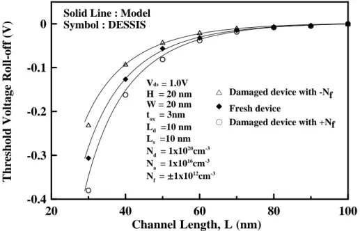
(12) compared with 2D numerical simulation results with the gate oxide thickness as a varied parameter..................................................................................................................................84 Fig.3.2.17 Analytical solution of the subthreshold current for Quadruple-gate MOSFETs compared with 2D numerical simulation results with the channel height as a varied parameter ..................................................................................................................................................84 Fig.3.2.18 Analytical solution of the subthreshold current for Quadruple-gate MOSFETs compared with 2D numerical simulation results with the workfunction a varied parameter. .85 Fig. 3.3.1 Schematic of QG MOSFETs: (a) three-dimensional device structure. With cut plane x direction and y direction, the device can be equivalently composed of 2 two-dimensional symmetrical double-gate (SDG) MOSFETs with width of W as shown in (b) with width of H as shown in (c). The two-dimensional device structures of Fig. 3.3.1 (b) and Fig. 3.3.1 (c) are used to derive the model, where regions 1, 3, and 2 denote the fresh and damaged zones, respectively ..............................................................................................................................89 Fig. 3.3.2 The dependence of channel potential on the normalized channel position for the different ratios of damaged zone to undamaged zone .............................................................93 Fig. 3.3.3 The variation of the two-dimensional potential distribution with the channel length and channel height for the simulation (The blue plot is for the damaged device with the positive trapped charges, the green plot is for the fresh device, and the red plot is for the damaged device with the negative trapped charges)................................................................93 Fig. 3.3.4 The variation of the two-dimensional potential distribution with the channel length and channel height for the model results (The blue plot is for the damaged device with the positive trapped charges, the green plot is for the fresh device, and the red plot is for the damaged device with the negative trapped charges)................................................................94 Fig. 3.3.5 Threshold voltage degradation versus normalized damaged zone for different thicknesses of silicon body ....................................................................................................100 Fig. 3.3.6 Threshold voltage degradation versus normalized damaged zone for different thicknesses of gate oxide. ......................................................................................................100 Fig. 3.3.7 Threshold voltage roll-off versus gate length for both fresh and damaged devices. ................................................................................................................................................101 Fig. 3.3.8 Threshold voltage degradation versus normalized damaged zone for DG, TG, and QG MOSFETs........................................................................................................................101 Fig. 3.3.9 ITSUBD versus normalized damaged zone for different silicon body thicknesses ................................................................................................................................................104 Fig. 3.3.10 ITSUBD versus normalized damaged zone for different gate oxide thicknesses104 xi.
(13) Fig. 3.3.11 SUBRUPversus gate length for the fresh and damaged devices. ........................105 Fig. 4.1.1 The three dimensional (3-D) structure for QG SOI MOSFETs.............................108 Fig. 4.1.2 The 3-D potential distribution with cut plane along y-z direction from the device simulator of DESSIS for Quadruple-Gate (QG) device of Vgs=0.2V and L=50nm ..............118 Fig. 4.1.3 The 3-D potential distribution with cut plane along y-z direction from the model results for Quadruple-Gate (QG) device of Vgs=0.2V and L=50nm......................................119 Fig. 4.1.4 The 3-D potential distribution with cut plane along y-z direction from the device simulator of DESSIS for Quadruple-Gate (QG) device of Vgs=0.2V and L=100nm. ...........119 Fig. 4.1.5 The 3-D potential distribution with cut plane along y-z direction from the model results for Quadruple-Gate (QG) device of Vgs=0.2V and L=100nm....................................120 Fig. 4.1.6 The variation of the central potential of Ф(x=W/2, y=H/2, z) with the normalized channel length position of z/Lg for the different gate biases(Vgs=0V~0.4V) ........................120 Fig. 4.1.7 The variation of the central potential of Ф(x=W/2, y=H/2, z) with the normalized channel length position of z/Lg for the different workfuntions..............................................121 Fig. 4.1.8 The variation of the central potential of Ф(x=W/2, y=H/2, z) with the normalized channel length position of z/Lg for the different channel heights. .........................................121 Fig. 4.1.9 Variation of minimum bottom potential with gate bias Vgs for different channel lengths.. ..................................................................................................................................123 Fig. 4.1.10 The dependence of threshold voltage roll-off ΔVth,QG and DIBL on channel length L for various gate oxide thicknesses.. ....................................................................................127 Fig. 4.1.11 The dependence of threshold voltage roll-off ΔVth,QG and DIBL on channel length L for various silicon widths... ................................................................................................128 Fig. 4.1.12 Analytical solution of subthreshold slope for the Quadruple-Gate (QG) device compared with 3D simulator results with the silicon film thicknesses as a varied parameter.. ................................................................................................................................................131 Fig. 4.1.13 Analytical solution of subthreshold slope for the Quadruple-Gate (QG) device compared with 3D simulator results with the gate oxide thickness as a varied parameter....132 Fig. 4.1.14 Analytical solution of subthreshold slope for the Quadruple-Gate (QG). device. compared with 3D simulator results the drain bias as a varied parameter.............................132 Fig.4.1.15 Analytical solution of the subthreshold current for Quadruple-gate MOSFETs compared with 2D numerical simulation results with the gate oxide thickness as a varied parameter................................................................................................................................134 Fig.4.1.16 Analytical solution of the subthreshold current for Quadruple-gate MOSFETs. xii.
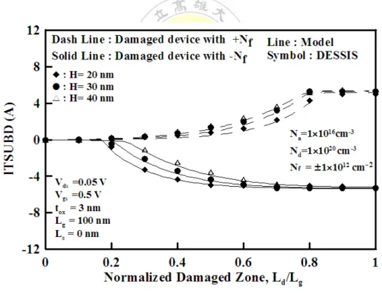
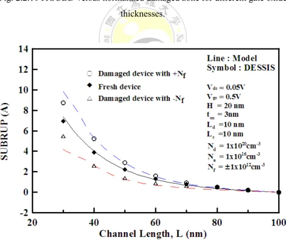
(14) compared with 2D numerical simulation results with the channel height as a varied parameter................................................................................................................................135 Fig. 4.1.17 Analytical solution of the subthreshold current for Quadruple-gate MOSFETs compared with 2D numerical simulation results with the workfunction a varied parameter.. ................................................................................................................................................135 Fig. 4.2.1 The three-dimensional (3-D) schematic view of a SOI quadruple-gate MOSFETs. With various trapped charge distributions, the channel can be divided into three regions. Regions 1 and 3 denote undamaged zone. Region 2 is damaged zone..................................137 Fig. 4.2.2 The dependence of channel potential on the normalized channel position for the different ratios of damaged zone to undamaged zone. ..........................................................155 Fig. 4.2.3 The variation of the two-dimensional potential distribution with the channel length and channel height for the simulation (The blue plot is for the damaged device with the positive trapped charges, the green plot is for the fresh device, and the red plot is for the damaged device with the negative trapped charges)..............................................................155 Fig. 4.2.4 The variation of the two-dimensional potential distribution with the channel length and channel height for the model results (The blue plot is for the damaged device with the positive trapped charges, the green plot is for the fresh device, and the red plot is for the damaged device with the negative trapped charges)..............................................................156 Fig. 4.2.5 Variation of minimum central potential with gate bias Vgs for different channel lengths... .................................................................................................................................158 Fig. 4.2.6 Threshold voltage degradation versus normalized damaged zone for different thicknesses of silicon body.....................................................................................................167 Fig. 4.2.7Threshold voltage degradation versus normalized damaged zone for different thicknesses of gate oxide... ....................................................................................................167 Fig. 4.2.8 Threshold voltage roll-off versus gate length for both fresh and damaged devices... ................................................................................................................................................168 Fig. 4.2.9 ITSUBD versus normalized damaged zone for different silicon body thicknesses... ................................................................................................................................................171 Fig. 4.2.10 ITSUBD versus normalized damaged zone for different gate oxide thicknesses... ................................................................................................................................................172 Fig. 4.2..11 SUBRUP versus gate length for the fresh and damaged devices... ....................172. xiii.
(15) Chapter 1 INTRODUCTION 1.1 Motive of the Thesis For decades, progress in device scaling has followed an exponential curve, with the device density on a microprocessor doubling every three years. This has come to be known as Moore's law [1]. In an ever increasing need for higher current drive and better short-channel characteristics, silicon-on-insulator (SOI) MOS transistors are evolving from classical, planar, single-gate devices into three-dimensional devices with multiple gates (double-gate, tri-gate or quadruple-gate devices). These devices offer a higher current drive per unit silicon area than conventional MOSFETs. In addition, they offer optimal short-channel effects (reduced DIBL and subthreshold slope degradation). As CMOS devices have been scaled down, the channel length shrinks and the absolute value of threshold voltage becomes smaller due to the reduced controllability of the gate over depletion region by the increased charge-sharing from the source/drain. The first publication describing a double-gate SOI MOSFET dates back to 1984. The Tri-Gate or FinFET is the recent solutions for controlling SCEs and improving the subthreshold swing as well as packing densities. A group of leading companies publishes their projections for the next decade in the most recent International Technology Roadmap for Semiconductors (ITRS) [4], This roadmap projects the gate-length of the devices about 25nm at the year 2014, However, scaling the gate-length beyond 25 nm would be much more difficult . Because it is close to the fundamental limits of semiconductor physics. The most important issue is how much further can the scaling of the devices be continued. Multi-gate field-effect transistors (MuGFETs) such as Tri-Gate, FinFETs, have a strong potential for sub 32 nm technologies, which is in agreement with the ITRS roadmap.. 1.
(16) Single gate. Triple gate. Double gate. Surrounding gate. Gate Gate Oxide. Silicon. Buried Oxide. Tri-gate FET. GAA,SON. SOI MOSFET. Mental. SiO2. MIGFET. Π-gate FET. FinFET. Ω-gate FET. Quadrupple gate FET. Surrounding gate FET. Silicon. Fig. 1.1 Different gate structures [2]. A numerous of literatures have modeled the hot-carrier-induced threshold voltage of planar and double-gate MOSFETs in the past decade. So far, very little work has been done on the analytical modeling of Quadruple-Gate (QG) MOSFETs including the localized interface trapped charges. Although there have been some works about the device performance through numerical simulation [5], or the device physics from experimental data [6]. To overcome limitations and realize high-performance MOS transistors, by considering effects of equivalent oxide charges on the flat-band voltage, effective conducting path, and poisson equation, a concise analytical subthreshold behavior model for QG MOSFETs with the interface trapped charges including threshold voltage, subthreshold slope, and subthreshold current are needed.. 2.
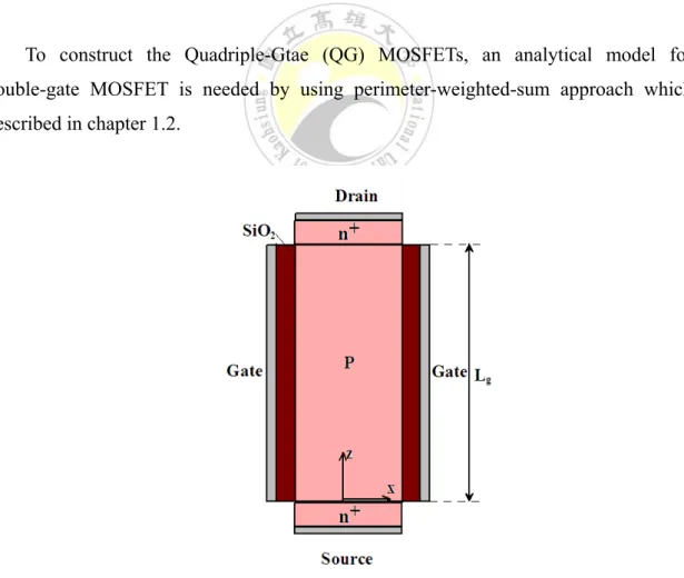
(17) 1.2 Quadruple-Gate Device Overview The Schematic of QG MOSFETs is shown in Fig. 1.2. The devices consist of four side gates on. To avoid solving for 3-D Poisson equation which is too complicated to be derived, the 3-D QG device can be replaced with two 2-D equivalent symmetric double-gate structures by ignoring the coupling effects for assuming that channel length/channel width and channel length/channel thickness is larger than 2 which fall within the restrictions required to obtain realistic and operational QG devices [7].. Fig. 1.2 Schematic of QG MOSFETs: (a) three-dimensional device structure, (b) with cut plane along x-direction (c) with cut plane along y-direction The device can be equivalently composed of two 2-dimensional symmetrical double-gate (SDG) MOSFET with width of W as shown in (b) and symmetrical double-gate (SDG) MOSFET with width of H as shown in (c). 3.
(18) A transition from bulk to multiple-gate fully depleted silicon-on-insulator (SOI) MOSFETs offers higher current drive per unit silicon area and better short-channel immunity. The QG device improves on the planar devices which reduce drain-source current leakage, and the control of the gates on the channel in a QG MOSFET is stronger than that in a conventional MOSFET as the gate voltage is applied from several sides and not just from the top. In recent years, multi-gate MOSFETs have received more attention than the planar MOSFETs in the high speed or high frequency applications. Comparing QG device to conventional bulk CMOS device at the same technology node, these non-planar devices are found to be competitive with similarly-sized bulk CMOS transistors. QG MOSFETs will be more promising for the future VLSI circuits. Therefore, exploitation and use of QG MOSFETs in memory circuits [7] require the physics-based transistor model [8-11]. The findings of the model are much useful to investigate hot-carrier-induced threshold voltage and offer the basic guidance for the design of memory device. Furthermore, three-dimensional (3-D) simulations of QG transistors with gate lengths down to 30 nm show that the 30 nm QG device remains fully depleted, with near-ideal subthreshold swing and excellent short channel characteristics, suggesting that the QG transistor could pose a viable alternative to bulk transistors in the near future [12].. 4.
(19) Chapter 2 TWO DIMENSIONAL SUBTHRESHOLD BEHAVIOR MODEL FOR SOI QUADRUPLE-GATE MOSFETs WITH/ WITHOUT LOCALIZED TRAPPED CHARGES 2.1 Quasi Two Dimensional Subthreshold Behavior Model for Quadruple -Gate MOSFETs 2.1.1 Model Derivation Instead of solving for the complicated 3-D Poisson’s equation, we present a subthreshold model for quadruple-gate Quadruple gate MOSFETs based on the minimum central potential derived from the scaling equation. where the Quadruple (QG) device with the appropriate aspect ratio can be broken into two equivalent double-gate (DG) transistors working in y-z and x-z planes, respectively.. Fig. 2.1.1 Schematic of QG MOSFETs with cut plane along x-direction.. 5.
(20) The p-channel Quadruple-Gate (QG) x-direction cross-section is shown in Fig. 2.1.1, the symbols and axes used for modeling are also indicated in this figure. We assume that the impurity density is uniform in the channel region. The channel potential distribution is expressed by Φ ( x, z ) . According to the Poisson equation, the channel potential distribution can be written as eq.(2.1.1).. ∂ 2Φ ( x, z ) ∂ 2Φ ( x, z ) qN a + = ∂x 2 ∂z 2 ε si. 0 ≤ x ≤ W , 0 ≤ z ≤ Lg. (2.1.1). Where Na is the uniform doping concentration of the silicon film, tox is the gate oxide thickness, W is the silicon film width, Lg is the device channel length, and the x-axis is perpendicular and the z-axis is parallel to the channel length, respectively. By using the parabolic potential approach to solve the two-dimensional Poisson’s equation, the potential vertical to the channel direction can be assumed by. Φ( x, z ) = C1 ( z ) + C2 ( z ) x + C3 ( z ) x 2. (2.1.2). that will satisfy the following boundary conditions : ⎧ ⎪ ⎪Φ ( x, z ) = C1 ( z ) = Φ c ( z ) ⎪⎪ ∂Φ ( x, z ) C = ox (Vgs − V fb − Φ s ( z )) ⎨ CsiW x =W / 2 ⎪ ∂x ⎪ ∂Φ ( x, z ) =0 ⎪ ⎪⎩ ∂x x=0. (2.1.3). where Φ c ( z ) is the central potential, Cox is the effective oxide capacitance per unit area, Csi is the bulk silicon capacitance per unit area, Φ s ( z ) is the surface potential, εsi is permittivity of silicon (εsi =11.7×8.85×10-14 ), εox is permittivity of oxide (εox =3.9×8.85×10-14), and Vfb is the flat-band voltage of gate bias given as the difference between gate material work function and silicon work function. 6.
(21) V fb = φM − φsi. (2.1.3.1). φsi is the silicon work function, which is given by φsi = χsi +. Eg 2q. − φB. (2.1.3.2). Where Eg is the silicon bandgap at 300 K, χsi is the electron affinity of silicon, φB is the Fermi potential (= VT × ln( N a ni ) ), VT is the thermal voltage (=kT/q), and ni is the intrinsic carrier concentration.. we can find the channel potential as the combination of the surface and central potentials. It yields Cox ⎧ 2 ⎪Φ ( x, z ) = Φ c ( z ) + C W 2 (Vgs − V fb − Φ s ( z )) x ⎪ si ⎨ ⎪Φ ( z ) = Φ ( z ) + 4Csi Φ c ( z ) + Cox (Vgs − V fb ) c ⎪⎩ s 4Csi + Cox. (2.1.4). symmetry of the channel potential along the x-direction. It yields. d 2Φ C ( x = 0, z ) 1 − 2 (Φ C ( x = 0, z ) − φc ) = 0 dz 2 λ. (2.1.5). with. 1. λ. 2. =. 8Cox 4W ε si + CoxW 2. (2.1.6). and. φc = Vgs − V fb −. 4W ε si + CoxW 2 8Cox. (2.1.7). where Φ( x = 0, z ) is the central potential, φc is the long channel central potential, and λ is the scaling length. 7.
(22) 2.1.2 Boundary Conditions Value Problem By solving the ordinary differential equation, the general solution of (2.1.5) can be expressed as. 1. z. Φ C ( z ) = ae λ + be. 1 − z. λ. + φc. (2.1.8). The coefficients of a and b in (2.1.8) can be determined by using the boundary conditions at the source/silicon junction and the drain/silicon junction. The potential at the source end is Φ ( x, z = 0) = Vbi. (0 ≤ x ≤ W ). (2.1.9). Where Vbi=VTln(NaNd/ni2) is the built-in potential at the interface between source/drain and channel and Vds is the drain bias. (A) The potential at the drain end is Φ ( x, z = Lg ) = Vbi + Vds. (0 ≤ x ≤ W ). (2.1.10). 2.1.3 Scaling Length Fig1 shows that Multi-Gate(MG) device can be broken into two equivalent DG devices working in parallel. According to the scaling theory and ENG theory, the central channel potential of the DG device should satisfy the following scaling equation (2.1.5). With 8Cox ⎧ 1 ⎪ λ 2 = 4W ε + C W 2 ⎪ DG1 si ox ⎨ 8Cox ⎪ 1 = 2 ⎪⎩ λDG 2 4 H ε si + Cox H 2. (2.1.11). W and H are the channel width and channel height.The concept of ENG for the MOSFETs is first proposed to by [13] and gives a measure of gate control capability 8.
(23) over the channel. The larger ENG provides the device with the better gate control over the channel in comparison to the smaller one. ENG for the Multi-Gate(MG) device can be defined as ENGMG =. λSG λMG. (2.1.12). Because the MG device can be broken into two equivalent DG devices, its ENG can be determined by adding up ENGs of both DG devices. It leads to ⎧ ENGQG = ENGDG1 + ENGDG 2 ⎪ 1 1 ⎨ 1 = + 2 2 ⎪λ λDG1 λDG 2 2 ⎩ QG. (2.1.13). Fig. 2.1.2 ENG, λ, Lmin and ρ, for SG, DG, RG, CG, and SRG MOSFETs, (Calculating parameters: H = W = 10 nm, tox = 1 nm,OUCF = 0.7 and minimum scaling factor α 0 = 3.16) [13]. 9.
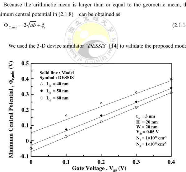
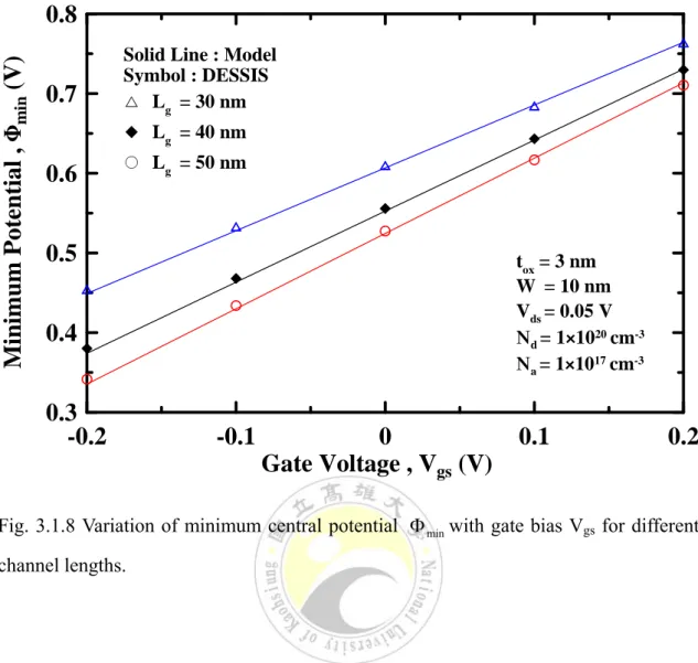
(24) 2.1.4 Minimum Central Potential From(2.1.8) (2.1.9) (2.1.10),They are obtained as follows: 1 1 − z − z ⎧ λQG λQG ⎪ e −1 Vds − (ω + Vbi )(e − 1) ⎪a = 2sinh( L / λ ) Vgs + 2sinh( L / λQG ) QG ⎪ ⎨ 1 1 z z ⎪ λQG λ e 1 V ( ω V )( e − − + − 1) bi ⎪b = Vgs − ds ⎪ 2sinh( L / λQG ) 2sinh( L / λQG ) ⎩. (2.1.14). where. ω = V fb +. 4W ε si + CoxW 2 16Cox. (2.1.15). Because the arithmetic mean is larger than or equal to the geometric mean, the minimum central potential in (2.1.8) can be obtained as Φ C . min = 2 ab + φc. (2.1.16). Minimum Central Potential , Fc,min (V). We used the 3-D device simulator "DESSIS" [14] to validate the proposed model.. 0.5 Solid line : Model Symbol : DESSIS . Lg = 40 nm. 0.4. & Lg = 50 nm. 0.3. + Lg = 60 nm. 0.2 tox = 3 nm H = 20 nm W = 20 nm Vds = 0.05 V Nd = 1â1020 cm-3 Na = 1â1016 cm-3. 0.1 0 -0.1 0. 0.1. 0.2 Gate Voltage , Vgs (V). 0.3. 0.4. Fig. 2.1.3 Variation of minimum central potential Φ min with gate bias Vgs for different channel lengths. 10.
(25) 2.1.5 Threshold Voltage Model The threshold voltage is defined as the gate voltage which causes the minimum central potential to become two times of bulk potential φB.Where φB is the difference between the Fermi level and intrinsic level of silicon in the neutral region. Under this condition, the inversion carrier density at the silicon surface equals the density of the doping atoms in the silicon bulk Na. This definition has been physically reasonable and successful in identifying the turn-on condition for bulk devices, where Na -values are in the range of 1×1016cm-3. The threshold voltage Vth can be obtained by solving for the gate voltage according to the criterion of Φ C . min =2φB. It leads to Vth =. 2( βγ + κα ) + ω − (2( βγ + κα ) + ω ) 2 − (1 − 4αγ )(ω 2 − 4 βκ ) 1 − 4αγ. Where 1 − z ⎧ λ ⎪α = e − 1 ⎪ 2sinh( L / λ ) ⎪ 1 − z ⎪ λ ⎪ β = Vds − (ω − 2φB + Vbi )(e − 1) ⎪ 2sinh( L / λ ) ⎪ 1 z ⎪ eλ − 1 ⎪ ⎨γ = 2sinh( L / λ ) ⎪ 1 ⎪ z ⎪ Vds − (ω − 2φB + Vbi )(e λ − 1) ⎪κ = − 2sinh( L / λ ) ⎪ ⎪ 4W ε si + CoxW 2 ⎪ω = 2φB + V fb + 16Cox ⎪ ⎪⎩. (2.1.17). (2.1.18). It should be pointed out for the long-channel device,that the coefficients for α and β approach zeros and (2.1.17) will be reduced to ω that is the threshold voltage for the long-channel QG FETs.. 11.
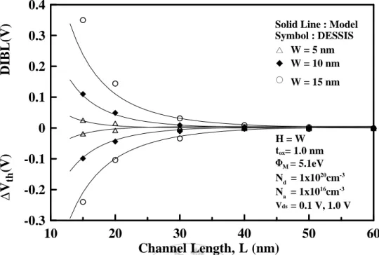
(26) DIBL(V). 0.16 Solid Line : Model Symbol : DESSIS - tox= 1.5 nm & tox= 1.0 nm. 0.12 0.08. + tox= 0.5 nm. 0.04 0. H = W = tsi= 10 nm FM = 5.1eV Nd = 1x1020cm-3 Na = 1x1016cm-3 Vds = 0.1 V, 1.0 V. ΔVth(V). -0.04 -0.08 -0.12 -0.16 10. 20. 30 40 Channel Length, L (nm). 50. Fig. 2.1.4 The dependence of threshold voltage roll-off ΔVth and DIBL on channel length L for various gate oxide thicknesses. Fig. 2.1.4 shows the dependence of threshold voltage roll-off and DIBL versus the channel length for various gate oxide thickness as a varied parameter and the data are compared with the 2D numerical simulation results. The threshold voltage roll-off (ΔVth) and DIBL predicted by the analytical solution is in good agreement with those from numerical simulation. The plot indicates that the threshold voltage roll-off and DIBL increase rapidly when the channel length decreases, particularly when the gate oxide thickness is increase to 1.5 nm. This implies that the gate gradually loses control of the channel as the gate oxide steadily increases its thickness, which prevents the vertical electric field from passing through the channel and brings about severe DIBL. Another efficient method to improve the degradation of the threshold voltage that is to make the silicon film thickness thinner as shown in Fig. 2.1.5. The plot indicates that the threshold voltage roll-off increase rapidly when the channel length decreases, particularly when the silicon widths is increase to 15 nm. Fig. 2.1.6 shows the threshold voltage roll-off versus the channel length for different channel heights and widths. It is revealed. that. among. H/W=9nm/9nm=1/1,. H/W=6nm/12nm=1/2,. and. H/W=2nm/16nm=1/8, H/W=1 will suffer the most threshold voltage roll-off and DIBL due to its largest natural length. although it improves current driving capability for its largest cross section area. To efficiently decrease threshold voltage roll-off and DIBL, 12.
(27) H/W should be small to produce a small natural length (in our case: H/W=2nm/16nm=1/8).. DIBL(V). 0.4 Solid Line : Model Symbol : DESSIS - W = 5 nm & W = 10 nm. 0.3 0.2. + W = 15 nm. 0.1. ΔVth(V). 0. H=W tox= 1.0 nm FM = 5.1eV Nd = 1x1020cm-3 Na = 1x1016cm-3 Vds = 0.1 V, 1.0 V. -0.1 -0.2 -0.3 10. 20. 30 40 Channel Length, L (nm). 50. 60. Fig. 2.1.5 The dependence of threshold voltage roll-off ΔVth,s and DIBL on channel length L for various silicon film widths.. DIBL(V). 0.12 0.08. Solid Line : Model Symbol : DESSIS 2H+2W= 36nm & H/W = 1. 0.04. . H/W = 1/2 + H/W = 1/8. ΔVth(V). 0. H = 10 nm tox = 1nm FM = 5.1eV Nd = 1x1020cm-3 Na = 1x1016cm-3 Vds = 0.1 V, 1.0V. -0.04 -0.08 -0.12 10. 20. 30 40 Channel Length, L (nm). 50. Fig. 2.1.6 The dependence of threshold voltage roll-off ΔVth,s on channel length L for different channel heights and widths. 13.
(28) Fig.2.1.7 shows the minimum channel length versus channel height (H) with the gate oxide thickness as a parameter. The comparison between DG, TG, and QG MOSFETs is carried out to meet the criterion of DIBL ≦50 mV.. Due to the best. immunity to SCEs , the QG device illustrates the shortest minimum channel length among the three MOSFETs. Furthermore, with H=W=20nm and tox=3nm, the QG FET illustrates an improvement up to 30%. and 20% in the minimum channel length. in comparison to DG and TG FETs, respectively. Minimum Channel Length L(nm). 60 50 40 30. Solid Line : Model Symbol : DESSIS DG : # tox= 1 nm DG : & tox= 0.5 nm TG : = tox= 1 nm TG : K tox= 0.5 nm QG : + tox= 1 nm QG : , tox= 0.5 nm DIBL=50mV H=W FM = 5.1eV Nd = 1x1020cm-3 Na = 1x1016cm-3 Vds = 0.1 V, 1.0V. 20 10 0 5. 10 15 Channel Height H(nm). 20. Fig.2.1.7 The minimum channel length versus channel height H with the gate oxide thickness as a parameter. The comparison between DG, TG, and QG devices is carried out to meet the criterion of DIBL ≦50mV. 14.
(29) 2.1.6 Subthreshold Current Model By substituting (2.1.16) into (2.1.4), the minimum surface potential for the QG device can be expressed by Φ s ,min = Φ c ,min +. 4Csi Φ c ,min + Cox (Vgs − V fb ) 4Csi + Cox. (2.1.19). With the combination of both the minimum surface potential and the minimum central potential, the minimum channel potential Φ ( x, z ) in (2.1.4) can be expressed as. Φ min ( x) = Φ c ,min +. Cox (Vgs − V fb − Φ s ,min ) x 2 2 CsiW. (2.1.20). Knowing the minimum channel potential solution of (2.1.20), we can proceed to derive the subthreshold current. Since the current density for the QG device flows predominantly in the z direction (from source to drain), the electron quasi-Fermi potential is essentially constant in the y-direction and is only function of x. By using the drift-diffusion approach , the current density (both drift and diffusion) together with the electron carrier density at the virtual cathode point can be written as. J n ( x, z ) = −qμn ⋅ ni ,min ( x, z ). dφn ( z ). (2.1.21). dz. With. ni ,min ( x, z ) = ni e. 1 [Φ min ( x , z ) −φn ( z )] VT. (2.1.22). where ni is the intrinsic carrier density. By integrating (2.1.21) in z and directions, the subthreshold current for the QG device can be obtained as. 15.
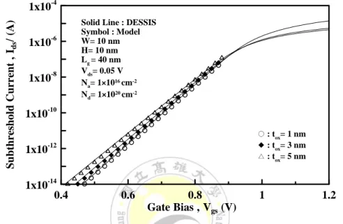
(30) H 2 0. I ds = ∫. ∫. W. 0. 2qμni e. 1 [Φ min ( x ) −φn ( z )] VT. d φn dxdy dz. (2.1.23). Where W is the channel width. Since the current is constant along the channel direction of z, integration of (2.1.23) with respect to z from 0 to yields Lg .. V Φ min ( x ) ⎡ − ds ⎤ H W VT 2 2qμVT ⎢1 − φn ( z )e ⎥ ∫ ∫ ni e VT dxdy ⎢⎣ ⎥⎦ 0 0 I ds = Lg Φ. c ,min V − ds ⎤ H ⎡ V VT 2 2WqμVT ⎢1 − φn ( z )e ⎥ ∫ ni e T ⎢⎣ ⎥⎦ 0 = Lg. =. ( x). Φ c ,min ( x ) V ⎡ − ds ⎤ VT W π qμVT ⎢1 − φn ( z )e ⎥ ni e VT ⎣⎢ ⎦⎥. Lg. Cox (−Vgs + V fb + Φ s ,min CsiVTW 2. −(. Cox CsiVT W 2. Erf (. H 2. ( −Vgs +V fb + Φ s ,min )) y 2. dy. Cox (−Vgs + V fb + Φ s ,min ) CsiVTW 2. (2.1.24). Shows the plots of subthreshold current model calculated from eq.(2.1.24) which are compared with those simulated from DESSIS of ISE-TCAD simulator. It is obviously seen that the analytical data from our model be in good agreement with 3-D simulation for different oxide thickness. To investigate how the gate oxide thickness affects the subthreshold current, Fig2.1.8 shows the dependence of the subthreshold current on the gate bias with the gate oxide thickness as a parameter. The thinnest gate oxide of tox=1 nm will suffer the least SCEs and brings about the smallest subthreshold leakage current among the three gate oxide thicknesses of tox=1 nm, 3 nm, and 5 nm. Fig. 2.1.9 shows the variation of subthreshold current with the different gate bias voltage with the silicon thickness as a varied parameter. It is obviously seen that as the thickness is reduced, the subthreshold current will be decreased. Fig. 2.1.10 shows the subthreshold current versus the gate bias for the different workfunction. The smallest workfunction of 4.1eV will cause the largest subthreshold leakage current among the 16.
(31) three workfunctions of 4.1eV, 4.6eV, and 5.1eV. Although a small workfunction of 4.1eV can result in large subthreshold current, it will induce a small flat-band voltage that is very useful for the low-power application circuits. The trade-off about how to take advantage of low-voltage operation without increasing the subthreshold leakage current must be taken into account as a small gate work-function is applied for the device.. Subthreshold Current , Ids/ (A). 1x10⁻⁴ 1x10⁻⁶ 1x10⁻⁸. Solid Line : DESSIS Symbol : Model W= 10 nm H= 10 nm Lg = 40 nm Vds= 0.05 V Na= 1â1016 cm-2 Nd= 1â1020 cm-2. 1x10⁻¹⁰ + : tox= 1 nm & : tox= 3 nm - : tox= 5 nm. -12. 1x10. 1x10-14 0.4. 0.6. 0.8 Gate Bias , Vgs (V). 1. 1.2. Fig. 2.1.8 The subthreshold current versus the gate bias for the different gate oxide thicknesses.. Subthreshold Current , Ids (A). 1x10⁻⁴ -6. 1x10. 1x10⁻⁸ -10. 1x10. Solid Line : DESSIS Symbol : Model W=H tox= 3 nm Lg = 40 nm Vds= 0.05 V Na= 1â1016 cm-2 Nd= 1â1020 cm-2 + : H = 10 nm & : H = 15 nm - : H = 20 nm. -12. 1x10. -14. 1x10. 0.2. 0.4. 0.6 0.8 Gate Bias , Vgs (V). 1. 1.2. Fig. 2.1.9 The subthreshold current versus the gate bias for the different silicon heights.. 17.
(32) Subthreshold Current , Ids(A). 1x10⁻⁴ 1x10⁻⁶ 1x10⁻⁸ 1x10⁻¹⁰. Solid Line : DESSIS Symbol : Model W = 10 nm H = 10 nm tox= 3 nm Lg = 40 nm Vds= 0.05 V Na= 1â1016 cm-2 Nd= 1â1020 cm-2. -12. 1x10. + : workfunction = 5.1 & : workfunction = 4.6 - : workfunction = 4.1. 1x10-14 -0.8 -0.6 -0.4 -0.2 0 0.2 0.4 0.6 Gate Bias , Vgs (V). 0.8. 1. 1.2. Fig. 2.1.10 The subthreshold current versus the gate bias for the different workfunction.. 18.
(33) 2.1.7 Subthreshold Slope Model An important parameter characteristic of subthreshold region for quadruple-gate MOSFETs operation is subthreshold swing. The quadruple-gate MOSFETs operation in the subthreshold region is commonly characterized by the inverse subthreshold slope factor (or subthreshold swing) and defined as S ( Swing ) =. dVgs. (2.1.25). d (log I ds ). Where Vgs is the gate voltage, Ids is the drain current, and Фmin is the surface minimum potential, and the influence of interface traps being neglected. The subthreshold slope (SS) is usually represented by the following classical expression.. Φ c ,min ⎛ Φ s ,min d Φ ⎞ d Φ c ,min VT s ,min ⎜e ⎟ × − e VT × dVgs dVgs d Φ s ,min ⎟ 1 ⎜ S ( Swing ) = ln10 × VT × ⎜ (1 − )⎟ − Φ s ,min Φ c ,min V V dV − − Φ ,min gs fb s gs ⎜ ⎟ VT (e VT − e VT ) ⎜ ⎟ ⎝ ⎠ (2.1.26). The central potential is larger than the surface potential for QG MOSFETs, which Φ c ,min. results in. e. VT. Φ s ,min. >> e. VT. . Therefore, (2.1.26)can be reduced to −1. ⎛ 1 d Φ c ,min d Φ s ,min ⎞ 1 S ( Swing ) = ln10 × ⎜ − (1 − )⎟ ⎜ V dV ⎟ − − Φ V V dV gs gs fb s ,min gs ⎝ T ⎠. (2.1.27). With ⎧ d Φ c ,min a 'b + b'a = + 1 ⎪ ab ⎪ dVgs ⎨ d Φ c ,min 4Cox ⎪ d Φ s ,min = 4Csi + ⎪ dVgs 4Csi + Cox dVgs 4Csi + Cox ⎩. 19. (2.1.28). −1.
(34) Where −L / λ ⎧ ' e g −1 = a ⎪ 2sinh( Lg / λ ) ⎪ ⎨ Lg / λ ⎪b' = 1 − e ⎪ 2sinh( Lg / λ ) ⎩. (2.1.29). The first term (ln10VT) in the above equation states that the subthreshold slope is 60~70mV/decade for a long channel device. The later term is due to the short channel effects. Fig. 2.1.11 shows analytical solution of the subthreshold slope for quadruple-gate MOSFETs compared with 2D numerical simulation results with the silicon film heights as a varied parameter, and good agreements are obtained. The plot indicates that the thinner silicon film for quadruple -gate MOSFETs has the smaller subthreshold slope than the thicker one does. It reveals that the degradation of subthreshold slope due to DIBL effect can be alleviated by the use of the thin silicon film. On the other hand, the subthreshold swing can also be substantially reduced by making use of the thinner gate insulator. Fig. 2.1.12 shows analytical solution of the subthreshold slope for quadruple -gate MOSFETs compared with 2D numerical simulation results with the gate insulator thickness as a varied parameter. The thinner insulator makes the gate capacitance smaller and implies lower subthreshold swing. It is found that quadruple -gate MOSFETs reduces DIBL effect and keeps swing of 60 decade/mV with long channel. Fig. 2.2.16 shows analytical solution of the subthreshold slope for quadruple-gate MOSFETs compared with 2D numerical simulation results for different drain biases. It is observed as the drain voltage changed from 0.05V to 2V the subthreshold swing value will not shift very quickly until the channel length is scaled down to 40nm.. 20.
(35) Subthreshold Slope, S(mv/dec). 130 120 110. Solid Line : Model Symbol : DESSIS . H = 10 nm & H = 15 nm. 100. + H = 20 nm. W=H tox = 3 nm Vds = 0.05 V Na = 1â1016 cm-3 Nd = 1â1020 cm-3. 90 80 70 60 20. 40 60 80 Channel Length, L (nm). 100. Fig. 2.1.11 Analytical solution of the subthreshold slope for QG MOSFETs compared with 2D numerical simulation results with the silicon film heights as a varied parameter.. Subthreshold Slope, S(mv/dec). 110 100 90. Solid Line : Model Symbol : DESSIS . tox = 1 nm & tox = 3 nm + tox = 5 nm. W = 10 nm H = 10 nm Vds = 0.05 V Na = 1â1016 cm-3 Nd = 1â1020 cm-3. 80 70 60 20. 40 60 80 Channel Length, L (nm). 100. Fig. 2.1.12 Analytical solution of the subthreshold slope for QG MOSFETs compared with 2D numerical simulation results with the gate oxide thickness as a varied parameter.. 21.
(36) Subthreshold Slope, S(mv/dec). 100. 90. Solid Line : Model Symbol : DESSIS . Vds = 0.05 V & Vds = 1 V. 80. + Vds = 2 V. W = 10 nm H = 10 nm tox = 3 nm Na = 1â1016 cm-3 Nd = 1â1020 cm-3. 70. 60 20. 40 60 80 Channel Length, L (nm). 100. Fig. 2.1.13 Analytical solution of the subthreshold slope for QG MOSFETs compared with 2D numerical simulation results with the drain bias as a varied parameter.. 22.
(37) 2.1.8 Results and Discussion Instead of solving for the complicated 3-D Poisson’s equation, we present a subthreshold model for quadruple-gate Quadruple gate MOSFETs based on the minimum central potential derived from the scaling equation,where the Quadruple (QG) device with the appropriate aspect ratio can be broken into two equivalent double-gate (DG) transistors working in y-z and x-z planes, respectively. Due to the increasing demand for high-performance and low-power-consumption ULSI technology, MOSFETs with sub-20-nm gate lengths are required [4]. As a result of reducing the device dimensions, new 3-D MOS structures with excellent tolerance to short-channel effects (SCEs) are needed. Quadruple-gate (QG) structures offers higher drive current and better immunity for SCEs compared to DG MOSFETs[16]. The feasibility to fabricate n- and p-channel QG MOSFETs has been demonstrated in recent work . The effects of different device parameters such as silicon film thickness, gate oxide thickness and drain bias on the model are thoroughly examined. To effectively suppress DIBL and SCEs, a thin oxide, a thin silicon film and a low drain bias can be applied to the device. It is shown that the proposed analytical model matches well with the numerical data over different device parameters. The accurate simulation results of the model make it useful for predicting the device subthreshold characteristics and offer guidance for the basic design of Quadruple-Gate (QG) SOI MOSFETs. Quantum effects are not considered here since the quantum-mechanical threshold-voltage variation needs to be taken into account when the silicon thickness drops below 8 nm [11]. It should be pointed out that although the quantum mechanical effects (QME) for the device is not accounted for in the model, it has been derived in the previous literatures that QME will pull up the threshold voltage due to the fact that quantum mechanical channel potential barrier is larger than classical channel potential barrier, which hence increase the gate voltage for inducing the free carrier inversion.. 23.
(38) 2.2 Quasi 2-D Subthreshold Behavior Model for SOI Quadruple-Gate MOSFETs with Localized Trapped Charges 2.2.1 Introduction ITRS (International Technology of Roadmap for Semiconductor) [4] has reported that there is a requirement to implement advanced non-classical CMOS structures to overcome the difficult challenges when the semiconductor technology node is below 16nm. Multi-Gate (MG) MOSFETs such as quadruple-gate (QG) MOSFET and FinFET with the non-planar gate can be one of the key solutions to well control the short-channel effects (SCEs), such as the subthreshold voltage roll-off, the drain-induced barrier lowering (DIBL), and the subthreshold-slope degradation, compared with planar MOSFETs. ITRS also reported that the reliability for the novel devices must be characterized for their leading-logic application. As the dimensions of MOSFETs are scaled down to the nanoscale regime, the hot-carrier effects (HCEs) on Multi-Gate MOSFETs is more obviously. Due to increasing the demand of high packing density of ULSI, the device dimension is needed to be further pushed into deep-submicrometer regime and the hot-carrier effects (HCEs) induced by the high electric field near the drain side will degrade the device/circuits performance [17][18]. HCEs will initiate the impact ionization, which will cause the unintentional gate and substrate leakage current when the accelerated carriers surmount the gate/buried oxide potential barrier and reach the gate and substrate terminals. Moreover, the hot-carrier-induced positive or negative charges can be trapped in the interface between the gate oxide and the silicon film, which can further cause the shift of the threshold voltage and deteriorate the electrical characteristic parameters of the device. Several studies have modeled the hot-carrier-induced threshold voltage of the planar and the double-gate MOSFETs in the past decade [19][20]. Recently, an analytical threshold voltage has been proposed for symmetrical nanoscale double-gate (DG) MOSFETs with an acceptor doping concentration Na=1016 cm-3, including only the effect of positive interface charges [21]. However, there is no thesis to investigate the threshold behavior 24.
(39) model of the quadruple-gate MOSFETs with the localized interface trapped charges. The quadruple-gate e MOSFETs that demonstrate the better short-channel controlling capability, higher current drive, and shorter scaling length than both planar and double-gate MOSFETs that will be more promising for the future ULSI circuits [22]. Further exploitation and use of quadruple-gate MOSFETs in memory circuits may require the physics-based transistor model. In this work, by considering the effects of equivalent oxide charges on the flat-band voltage [23], we report a novel short-channel analytical threshold behavior model for the quadruple-gate MOSFETs with localized trapped charges based on the exact two-dimensional (2-D) solution of Poisson equation and perimeter-weighted-sum approach [24]. The proposed model is verified by the three-dimensional (3-D) numerical simulation DESSIS of ISE-TCAD and explicitly illustrates how the various localized trapped charge conditions and the device structure parameters affect the potential distribution, and threshold voltage behavior. The findings of the model are much useful to investigate hot-carrier-induced threshold voltage and offer the basic guidance for the design of the quadruple-gate charge-trapped memory device. With the effects of interface trapped charges on the flat-band voltage, we report a novel quasi-3D interface-trapped-charge-induced threshold voltage model for quadruple-gate (QG) MOSFETs based on the scaling equation including equivalent number of gates (ENG). Quantum effects are not considered here since the quantum-mechanical threshold-voltage variation needs to be taken into account when the silicon thickness drops below 8 nm [11]. It should be pointed out that although the quantum mechanical effects (QME) for the device is not accounted for in the model, it has been derived in the previous literatures that QME will pull up the threshold voltage due to the fact that quantum mechanical channel potential barrier is larger than classical channel potential barrier, which hence increase the gate voltage for inducing the free carrier inversion.. 25.
(40) 2.2.2 Model Description The schematic of the 3-D quadruple-gate (QG) MOSFETs is shown in Fig. 2.2.1(a). Figs. 2.2.1(b) and 2.2.1(c) are the two-dimensional (2-D) device structure to derive the model. With various trapped charge distributions, the channel can be divided into three regions. Regions 1 and 3 denote undamaged zone. Region 2 is damaged zone. 3-D simulations are computationally more expensive and are not acceptable for compact modeling in comparison to 2-D simulations. To avoid solving for 3-D Poisson equation, 3-D QG device can be genuinely replaced with the two 2-D equivalently symmetric double-gate structures.. Fig. 2.2.1 Schematic of quadruple-gate MOSFETs: (a) three-dimensional device structure. With cut plane x direction and y direction, the device can be equivalently composed of 2 two-dimensional symmetrical double-gate (SDG) MOSFETs with width of W as shown in (b) with width of H as shown in (c). The two-dimensional device structures of Fig. 2.2.1 (b) and Fig. 2.2.1 (c) are used to derive the model, where regions 1, 3, and 2 denote the fresh and damaged zones, respectively. 26.
(41) 2.2.3 Quasi 2-D Generalized Potential Model The coupling effects between 2-D equivalently two symmetric double-gate structures can be ignored by the fact that channel length (Lg)/channel width (W) and channel length (Lg)/channel thickness (H) are larger than 2, which fall within the restrictions required to obtain realistic and operational QG devices [8]. Since the most leaky path is along the central of the channel for the 3-D QG device (i.e., at the position of (x=W/2, y=H/2, z), the 3-D potential of Φ(x=W/2, y=H/2, z) can be equivalently decomposed of 2-D central potential of Φ(x=W/2, z) for 2 symmetrical double-gate (SDG) MOSFET. Based on the exact two-dimensional (2-D) solution of Poisson equation, the central potential Φc,i(z) (i=1,2,3) for SDG MOSFET can be expressed as. Φ c ,1 ( z ) = a1e. z. −z. λQG. λQG. Φ c ,2 ( z ) = a2e. Φ c ,3 ( z ) = a3e. + b1e. + φc ,1. z. −z. λQG. λQG. + b2e. z. −z. λQG. λQG. + b3e. (2.2.1). + φc ,2. (2.2.2). + φc ,3. (2.2.3). 2 λQG. (2.2.4). 2 λQG. (2.2.5). 2 λQG. (2.2.6). with. φc ,1 ( z ) = Vgs − V fb1 −. qN a. φc ,2 ( z ) = Vgs − V fb 2 −. qN a. φc ,3 ( z ) = Vgs − V fb 3 −. qN a. ε si. ε si. ε si. Where. 27.
(42) coth(kLg ) − 1 qN kL {[cosh(kL1 − kLg ) − cosh(kL2 − kLg )](− f ) + (Vds + Vbi − φc1 )e g − Vbi + φc1} 2 Cox (2.2.7). a1 =. a2 =. k (2L − L ) coth(kLg ) −1 qN qN kL qN ekL2 e g 2 {[cosh(kL1) − − ](− f ) + (Vds + Vbi − φc2 + f )e g + φc2 −Vbi − f } 2 2 2 Cox Cox Cox (2.2.8). a3 =. coth( kLg ) − 1 2. {[cosh( kL1 ) − cosh( kL2 )]( −. qN f C ox. ) + (Vds + Vbi − φc 3 ) e. kLg. − Vbi + φc1} (2.2.9). b1 =. csch(kLg ) 2. {[cosh(kL2 − kLg ) − cosh(kL1 − kLg )](−. qN f Cox. ) + (Vbi − φc1 )e. kLg. − Vbi − Vds + φc 3} (2.2.10). b2 =. k(2L −L ) coth(kLg ) −1 qN kL qN 2kL ekL2 −e g 2 −qNf 2kL {[−cosh(kL1)e g + ]( ) +(−Vds −Vbi +φc2 − f )e g +(−φc2 −Vbi + f )e g } 2 2 Cox Cox Cox (2.2.11). b3 =. coth(kLg ) − 1 2. kL. kL. e g {e g [cosh(kL2 ) − cosh(kL1 )](−. qN f Cox. ) + (Vbi − φc1 )e. kLg. − Vbi − Vds + φc 3} (2.2.12). from (2.1.13) , let H=W. λQG =. 4W ε si + CoxW 2 16Cox. (2.2.13). from (2.1.4) Φ s ,1 ( z ) = Φ c ,1 ( z ) +. 4Csi Φ c ,1 ( z ) + Cox (Vgs − V fb ,1 ). Φ s ,2 ( z ) = Φ c ,2 ( z ) +. Φ s ,3 ( z ) = Φ c ,3 ( z ) +. 4Csi + Cox 4Csi Φ c ,2 ( z ) + Cox (Vgs − V fb ,2 ) 4Csi + Cox 4Csi Φ c ,3 ( z ) + Cox (Vgs − V fb ,3 ) 4Csi + Cox 28. (2.2.14). (2.2.15). (2.2.16).
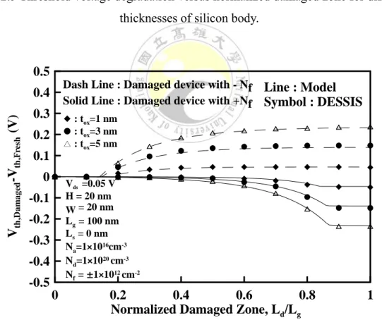
(43) With the parabolic potential approach, the channel potential Φ i that comprises the surface potential Φ s ,i and the central potential Φ c ,i can be written as[19] Φ i ( x) = Φ c ,i +. Cox (Vgs − V fb , i − Φ s ,i ) x 2 2 Csi H. (2.2.17). Where Na is the uniform doping concentration of the silicon film, tox is the gate oxide thickness, tbox is the buried oxide thickness, tsi is the silicon film thickness, εsi is the dielectric constant of silicon (εsi=11.7×8.85×10-14 ), εox is permittivity of oxide (εox=3.9×8.85×10-14), Vgs is the top gate bias, Vsub is the substrate bias, and Vfb1=Vfb3 is the flat-band voltage in the undamaged regions. In the damaged region, due to the effect of equivalent oxide charges on the flat-band voltage, we obtain V fb 2 = V fb1 −. qN f 1 tox x ρ ( x) dx + Qit ] = V fb1 − [∫ 0 Cox tox Cox. (2.2.18). where ρ(x) is localized oxide charge density assumed zero for simplicity, Cox is the gate oxide capacitance per unit area, and Qit=qNf is the uniform localized interface trapped charge density. To verify the proposed model, the published 3-D device simulator, “DESSIS”, is performed to simulate the device. Fig. 2.2.2 shows the dependence of channel potential on the normalized channel position for the different ratios of damaged zone to undamaged zone. As the length of the damaged zone increases, the deformation of the potential barrier increases. In the case of the negative interface fixed charges, the minimum bottom potential appears in the damaged zone, whereas in the case of the positive interface fixed charges, it appears in the undamaged zone. This implies that a large Vth shift would be observed in the former case. Fig. 2.2.3 and Fig. 2.2.4 show the dependence of potential distribution on both of the channel length and channel height with the damaged and fresh devices for the simulation and the model results. The good match between the simulation and model results is obtained. It is shown that the damaged device with positive trapped charges will decrease the potential barrier between the source and drain side in comparison to the fresh device. It will increase the 29.
數據
+7
相關文件
細目之砂紙,將絕緣體 及內部半導電層鉛筆狀
①尼古丁 ②焦油 ③一氧化碳
有人說「血液中之二氧化碳含量應該維持一定」 ,你認為這樣
Niemeyer, ‘a generalized approach to partial discharge modeling’, IEEE transactions on
導體 絕緣體 電解質 非電解質.
導體 絕緣體 電解質 非電解質.
導體 絕緣體 電解質 非電解質.
酸性氣體(二氧化硫、二氧化氮)可以飄浮到離源頭很遠的地
![HPSH [ 氧化數平衡反應式係數 ]](data:image/gif;base64,R0lGODlhAQABAIAAAP///wAAACH5BAEAAAAALAAAAAABAAEAAAICRAEAOw==)