Oxide Roughness Effect on Tunneling
Current of MOS Diodes
B.-C. Hsu, Student Member, IEEE, K.-F. Chen, C.-C. Lai, S. W. Lee, and C. W. Liu, Senior Member, IEEE
Abstract—Two-dimensional (2-D) device simulation is used to investigate the tunneling current of metal ultra-thin-oxide silicon tunneling diodes with different oxide roughness. With the conformal nature of ultrathin oxide, the tunneling current density is simulated in both direct tunneling and Fowler–Nordheim (FN) tunneling regimes with different oxide roughness. The results show that oxide roughness dramatically enhances the tunneling current density and the 2-D electrical effect is responsible for this increment of tunneling current density. Furthermore, a set of devices with controlled oxide roughness is fabricated to verify the simulation results and our model qualitatively agrees with the experiment results.
Index Terms—Device simulation, metal–oxide–silicon diode (MOS), roughness, tunneling current.
I. INTRODUCTION
T
HE scaling of metal–oxide–semiconductor (MOS) tran-sistors requires the gate oxide thickness to be less than 3 nm. For this ultrathin oxide, the oxide roughness is no longer negligible, and has a significant effect on gate current. Sev-eral groups have reported that the oxide roughness have ef-fects on device characteristics in many ways, such as degrading MOSFET channel mobility [1], lowering the reliability of the gate insulator [2], [3], and increasing the gate tunneling current [3]. However, the oxide thickness studied in these papers [1]–[3] is too thick (4.1 nm–25 nm) and the tunneling current is focused on the Fowler–Nordheim (FN) tunneling regime. Recently, our group reported that the oxide roughness enhances the electrolu-minescence from NMOS tunneling diodes [4], and increases the oxide reliability during electrical stress [5]. For ultrathin oxide ( 1.6 nm), Ting et al. [6] have studied the interface roughness effect on the tunneling gate current in MOS tunneling structures, the roughness model used in this study [6], [7] assumes that the SiO /Si interface roughness would induce a nonuniform distri-bution of oxide thickness with flat oxide surface [see Fig. 1(a)]. However, the assumption is not correct. Zafar et al. [8] have reported that the oxide films will grow conformally over the roughened Si surface at least for the first 5 nm [see Fig. 1(b)]. Other reports also indicated that the surfaces of oxide filmsManuscript received June 3, 2002; revised September 19, 2002. This work was supported by National Science Council, Taiwan, R.O.C., under Contract 90-2212-E-002-224 and Contract 90-2212-E-002-226. The review of this paper was arranged by Editor J. M. Vasi.
B.-C. Hsu, K.-F. Chen, C.-C. Lai, and C. W. Liu are with the Graduate Institute of Electronics Engineering and Department of Electrical Engineering, National Taiwan University, Taipei, Taiwan, R.O.C. (e-mail: f8921012@ ee.ntu.edu.tw; [email protected]).
S. W. Lee is with the Department of Materials Science and Engineering, Na-tional Tsing Hua University, Hsinchu, Taiwan, R.O.C.
Digital Object Identifier 10.1109/TED.2002.805229
grown at high temperatures have a surface morphology similar to that of the original substrate [9]. Furthermore, the Si/oxide interface under controlled oxidation conditions has showed the same surface morphology as original substrates [10]–[12]. In this paper, we confirm that the ultrathin gate oxide ( 3 nm) is growth conformally, and the commercial two-dimensional (2-D) device simulator, MEDICI [13], is used to simulate the de-vice characteristics. Furthermore, a set of dede-vices is fabricated to verify the simulation results. The surface roughness is con-trolled by the very high vacuum (VHV) pre-bake and the oxide surface morphology is measured by atomic force microscope (AFM).
II. EXPERIMENTS ANDDEVICESIMULATIONDETAILS A. Experiments
The ultrathin gate oxide is grown by rapid thermal oxidation on 1 10 -cm n-type wafers at 800 850 C. The gas flows are 500 sccm nitrogen and 500 sccm oxygen at a reduced pres-sure. For rough oxide growth, the Si substrate is prebaked in VHV ( torr) at 1000 C for 2 min after HF dip, while the flat oxide has no such VHV prebake. Note this VHV pre-bake should yield a clean Si surface [14]. The oxide growth is conducted after the hydrogen bake, which creates hydrogen pas-sivated surface, and subsequently nitrogen post-oxide-anneal (POA) is performed at 900 C for 10 min. The oxide thickness is measured by ellipsometry and the surface roughness is sured by AFM. The Si/oxide interface roughness was also mea-sured by AFM by using HF to remove the oxide. The PMOS tunneling diodes had Al gate electrodes with circular areas of
cm defined by photolithography. B. Rough Oxide Model
MEDICI [13] is used in the 2-D device simulation. The con-formal ultrathin oxide is modeled on an n-type Si substrate. The oxide model is given in Fig. 1(d). The tiny steps indicate atomic discontinuity at oxide surface and interface. The substrate is n-type with a doping concentration of cm . The ultra-thin oxide has equal thickness in the vertical direction and the roughness morphology is simply described by two parameters, and . is the roughness variation on the oxide surface and interface, and is the distance between two peaks on surface, or the roughness period. After defining the oxide morphology, 300-nm aluminum gate is defined as the gate electrode. C. Gate Current Models
When analyzing the direct tunneling current density, MEDICI [13] computes the net tunneling current density due 0018-9383/02$17.00 © 2002 IEEE
Fig. 1. Different oxide models: (a) is used by Sune et al. ([7]); (b) is used by Zafar et al. ([8]); (c) the electric field of a flat MOS structure; and (d) the illustration of (2-D) electrical effect in the rough oxide. The electric field is not along the growth direction. TheH represents the roughness height (nm) and T represents the roughness period (nm).
to electrons tunneling from the conduction and valence band of a semiconductor or electrode, through an insulator, into the conduction band of another semiconductor or electrode. During the simulation process, the tunneling path where the tunneling current occurs is determined by locating the closest point on the opposing boundary. This simplification allows the Wentzel–Kramers–Brillouin (WKB)-type calculation in the device simulator. The tunneling model in MEDICI [13], [15] combines both the direct tunneling regime and the FN regime. The net tunneling current across the insulator is calculated using the independent electron approximation and the conduction band electron tunneling (CBET) current is given by [16]
(1)
where the integral is over the kinetic energy of the incident
electrons. and are the electron quasi-Fermi
level, the conduction band edge, and the electron effective tunneling mass of silicon substrate, respectively. and are the corresponding electron quasi-Fermi level and conduction band edge in gate electrode. The endpoint of the integration is determined by the barrier height . is the electron charge, is Planck’s constant, is the thermal energy, and TC is the tunneling coefficient of an electron with energy . To obtain sufficient accuracy, the Gundlach formula is used to calculate exact tunneling coefficient of a trapezoidal barrier [17]. During the simulation, the simulator calculates the electric field and potential for every node and automatically computes the tunneling current density at each node through the shortest path. To confirm the simulation accuracy, the structures with the same roughness conditions and oxide thickness but
different device lengths (numbers of periods) were simulated. The results show that the tunneling current density is proportion to the number of periods, which indicates that the mechanism of tunneling through the shortest path is taking place in each period. Therefore the total current density can be obtained by multiplying the number of periods to the current density of the device with one period. Note that the gate current model used for simulation did not consider the complete quantum effects since we have no idea to do the 2–D QM simulation.
III. RESULTS ANDDISCUSSION A. Experiment Results
The correlation between oxide surface roughness and oxide/Si interface roughness can be found in [18, Fig. 7] (not shown here). The interface roughness is measured by AFM right after HF dip. The slope close to unity indicates the conformal growth of oxide, which agrees with the results reported by Tsai et al. [19]. In this paper, the roughness value is calculated from AFM measurement program and is defined as the coordinate average value of the surface roughness within the area being analyzed
Roughness (2)
where
Fig. 2 shows the TEM cross section photo of the MOS diode with rough oxide/Si surface. The photo also shows that the oxide is conformal. However, the small roughness with small period ( nm) cannot be distinguished from the TEM photo due to the resolution limit and the sample thickness. The TEM image is a projection along the TEM sample thickness ( 100 nm), and the small period of roughness is smeared out.
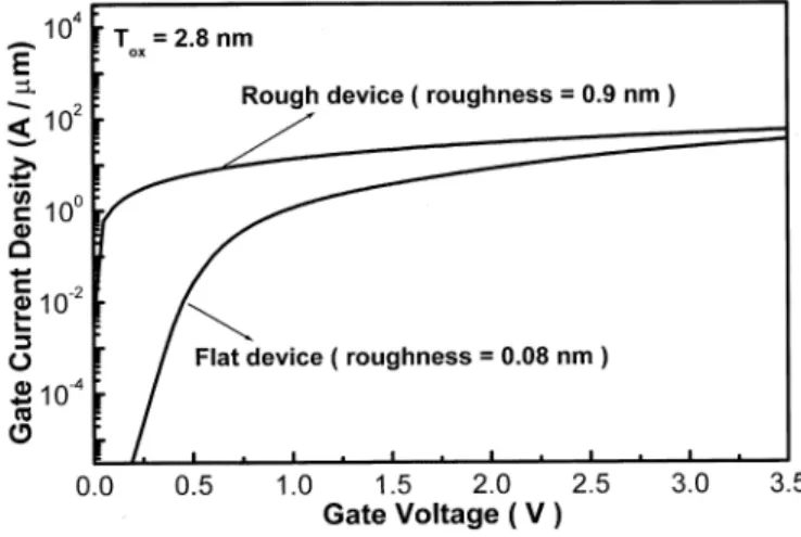
Fig. 3 shows the current–voltage ( ) characteristics of the PMOS tunneling diodes with rough and smooth oxide under accumulation bias (positive voltage at the gate). Note that the transport mechanism of inversion current is given in [20]. The device with a rough oxide (roughness nm) has a larger gate tunneling current as compared to the device with a smooth oxide (roughness nm). Both devices have the similar oxide thickness of 2.8 nm, measured from ellipsometry. Both di-rect and FN tunneling current increases for the rough oxide, and the changes of accumulation current between these two diodes is more significant in the direct tunneling region than in the FN tunneling region. This feature is quite different from the simu-lation results of Ting et al. [6], where the accumusimu-lation current continuously increases in the DT region but first increases and then decreases in the FN tunneling region as interface roughness increases. The discrepancy may be due to the incorrect oxide model [see Fig. 1(a)] used in Ting’s work. This feature is not due to series resistance effect, since the substrate doping increases to 10 cm , the phenomenon is still observed in simulation.
Fig. 2. TEM photo of a rough oxide prepared by VHV prebake.
Fig. 3. I0V characteristics of the PMOS tunneling diodes with rough and smooth interfaces under positive gate bias withT = 2:8 nm.
B. Simulation Results and Discussion
The simulated curves for MOS tunneling diodes with different interface roughness characterized by the value of are shown in Fig. 4. The roughness period is fixed to 1 nm. For comparison, we also include a reference structure with a smooth interface . The conformal oxide thickness used in the simulation is 2.5 nm, which is obtained by fitting the curve of the flat device in Fig. 3 with . The inset of Fig. 4 shows the fitting results. Note that the oxide roughness model used in the 2–D simulation is described as two parameters and , and assumed no roughness in the third direction. However, the true device has three dimensions and the three-dimensional
Fig. 4. Simulated I0V characteristics for PMOS tunneling diodes with different oxide roughness (H). The inset shows the fitting between the simulation curve (H = 0; T = 2:5 nm) and experiment data.
(3-D) electrical effect will be more complicated than the 2-D electrical effect we discussed. Therefore, the and values of a device cannot be fully determined from the AFM pictures even if we have all the surface roughness information down to the angstrom resolution and statistically average all the data points. All of these effects lead to the error between the experiment data and simulation curve in Fig. 4.
From Fig. 4, the gate tunneling current density increases sig-nificantly with increasing . Fig. 5 shows the gate current den-sity ratio versus different roughness conditions characterized by
Fig. 5. Gate current density ratio versus different oxide roughness(H). the roughness height, . The gate current density ratio is de-fined as the ratio of the gate tunneling current density of a rough device to that of a flat device . The gate current density ratio in the DT regime ( V) is more sensitive to oxide roughness and reaches 23 for nm. In FN tunneling region ( V), the ratio is only 11 for nm. The large effective area on the rough oxide could be responsible to the gate current density increase. However, the effective area ratio of rough oxide to smooth oxide is calculated to be about
1.56 for nm and nm. This number is too small
to explain the large gate current density ratio.
Fig. 1(c) and (d) illustrates the simulated electric field of the devices with flat and rough oxides, respectively. The vectors represent the direction and magnitude of electric field within a period. For a flat oxide [see Fig. 1(c)], the electric field is one-dimensional (1-D) and is along the growth direction ( di-rection). However, when the interface is no longer smooth [see Fig. 1(d)], both the shortest distance between the oxide surface and oxide/Si interface and the electric field are no longer along the growth direction, which means that the electric field has a component in the direction. This 2-D electric field will cause electrons tunneling through the oxide by the shortest paths 2 and 3, not path 1. Therefore, the maximum electrical field in the rough oxide increases as the roughness increases, and its direction is no longer along the growth direction. The 2-D elec-trical effect is responsible for the large gate current density ratio, since the gate current density is a strong function of electrical field in the 1-D model.
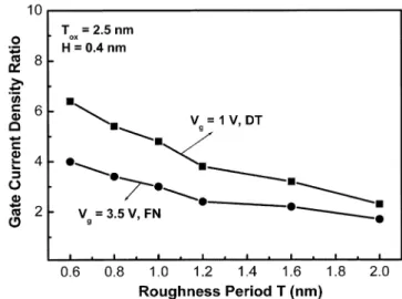
The gate tunneling current density ratio versus different
roughness period is shown in Fig. 6 with nm.
The ratio is larger in the direct tunneling regime ( V), as compared to FN tunneling region. The gate current density ratio decreases as increases, since the large indicates smooth surface.
Fig. 7 shows the simulated gate current density ratio versus the oxide thickness. The simulated roughness height is 0.4 nm and roughness period is 1 and 2 nm, respectively. As the conformal oxide thickness increases, the gate current density ratio first increases and then decreases slightly. For devices with nm, the trend is not obvious since the roughness is small
Fig. 6. Gate current density ratio versus the roughness period(T ).
Fig. 7. Gate current density ratio versus the oxide thickness.
Fig. 8. Schematics of the short distance for (a) thick, (b) moderate, and (c) thin oxide.
as compared to the devices with the same oxide thickness but nm. This can be explained by the shortest distance argu-ment (see Fig. 8). The relative decreargu-ment of shortest distance be-tween oxide surface and interface is small for thin oxide; while only beyond some moderate oxide thickness, the relative decre-ment is effective.
IV. CONCLUSION
A simple but relatively accurate oxide model is used in the gate tunneling current density simulation. The oxide model is based on conformal nature of oxide growth. With the roughness height parameter and roughness period parameter , the gate tunneling current density can be investigated by a 2-D de-vice simulator. Due to the 2-D electrical effect, the increasing roughness height with fixed roughness period can significantly increase the gate tunneling current, and for a given roughness height, the current increases first and drops a little as the period parameter increases. Our model qualitatively agrees with the ex-periment results. Due to the randomness nature of oxide rough-ness, the accurate modeling of the gate current is very compli-cated.
ACKNOWLEDGMENT
B.-C. Hsu would like to thank United Manufactory Company (UMC) for fellowship support.
REFERENCES
[1] J. Koga, S. Takagi, and A. Toriumi, “A comprehensive study of MOSFET electron mobility in both weak and strong inversion regimes,” in IEDM. Tech. Dig., 1994, pp. 11–14.
[2] M. Miyashita, M. Itano, T. Imaoka, I. Kawanabe, and T. Ohmi, “Depen-dence of thin oxide films quality on surface micro-roughness,” in VLSI
Tech. Dig., 1991, pp. 45–46.
[3] T. Nakanishi, S. Kishii, A. Ohsawa, and K. Honda, “Degradation of time-dependent dielectric breakdown characteristics of MOS capacitors by silicon surface roughness,” in VLSI Tech. Dig., 1989, pp. 79–82. [4] C. W. Liu, M. H. Lee, M. J. Chen, C.-F. Lin, and M. Y. Chern,
“Rough-ness-enhanced electroluminescence from metal–oxide–silicon tunneling diodes,” IEEE Electron Device Lett., vol. 21, pp. 601–603, Dec. 2000. [5] C.-H. Lin, F. Yuan, C.-R. Shie, K.-F. Chen, B.-C. Hsu, M. H. Lee, W. W.
Pai, and C. W. Liu, “Roughness-enhanced reliability of MOS tunneling diodes,” IEEE Electron Device Lett., vol. 23, pp. 431–433, July 2002. [6] D. Z.-Y. Ting, “Tunneling characteristics of nonuniform ultrathin
ox-ides,” Appl. Phys. Lett., vol. 73, pp. 2769–2771, 1998.
[7] J. Sune, I. Placencia, E. Farras, N. Barniol, and X. Aymerich, “On the Si-SiO interface roughness in VLSI-MOS structures,” Phys. Stat. Sol.
A, vol. 109, pp. 479–491, 1988.
[8] S. Zafar, Q. Liu, and E. A. Irene, “Study of tunneling current oscillation dependence on SiO thickness and Si roughness at the Si/SiO inter-face,” J. Vac. Sci. Technol. A, Vac. Surf. Films, vol. 13, pp. 47–53, 1995. [9] M. Suzuki, Y. Homma, Y. Kudoh, and N. Yabumoto, “Roughness eval-uation of thermally oxidized Si (111) surfaces by scanning force mi-croscopy,” Jpn. J. Appl. Phys., pt. 1, vol. 32, pp. 1419–1422, 1993. [10] G. J. Pietsch, U. Kohler, O. Jusko, M. Henzler, and P. O. Hahn,
“Structure of the stepped Si/SiO interface after thermal oxidation: Investigations with scanning tunneling microscopy and spot-profile analysis of low-energy electron diffraction,” Appl. Phys. Lett., vol. 60, pp. 1321–1323, 1992.
[11] Y. Homma, M. Suzuki, and N. Yabumoto, “Observation of atomic step morphology on silicon oxide surfaces,” J. Vac. Sci. Technol. A, Vac. Surf.
Films, vol. 10, pp. 2055–2058, 1992.
[12] G. S. Shekhawat, R. P. Gupta, S. S. Shekhawat, D. P. Runthala, P. D. Vyas, P. Srivastava, S. Venkatesh, K. Mamhoud, and K. B. Garg, “Scan-ning tunneling microscopy of Si/SiO interface roughness and its de-pendence on growth conditions,” Appl. Phys. Lett., vol. 68, pp. 114–116, 1996.
[13] “MEDICI,” Technology Modeling Assoc., Palo Alto, CA.
[14] F. W. Smith and G. Ghidini, “Reaction of oxygen with Si(111) and (100): Critical conditions for the growth of SiO ,” J. Electrochem. Soc., vol. 129, pp. 1300–1306, 1982.
[15] MEDICI User’s Manual, pp. 2-103–2-109. Ver. MD 2000.2.
[16] W. Harrison, “Tunneling from an independent-particle point of view,”
Phys. Rev., 1961.
[17] K. H. Gundlach, “Zur berechnung des tunnelstroms durch eine trapez-formige potentialstufe,” Solid State Electron., vol. 9, pp. 949–957, 1966. [18] C.-H. Lin, M. H. Lee, B.-C. Hsu, K.-F. Chen, C.-R. Shie, and C. W. Liu, “Oxide roughness enhanced reliability of MOS tunneling diodes,” in Proc. Int. Semiconductor Device Research Symp., 2001, pp. 46–49. [19] V. Tsai, X.-S. Wang, E. D. Williams, J. Schneir, and R. Dixson,
“Con-formal oxides on Si surfaces,” Appl. Phys. Lett., vol. 71, pp. 1495–1497, 1997.
[20] C.-H. Lin, B.-C. Hsu, M. H. Lee, and C. W. Liu, “A comprehensive study of inversion current in metal-oxide-silicon tunneling diodes,”
IEEE Trans. Electron Devices, vol. 48, pp. 2125–2130, Sept. 2001.
B.-C. Hsu (S’01) received the B.S. degree from National Taiwan University, Taipei, Taiwan, R.O.C., in 1999. He is currently pursuing the Ph.D. degree in electrical engineering at the same university.
His current research interests include the MOS tunneling photodetectors for 850-, 1300-, and 1550–nm applications, improvement of reliability on MOS devices by deuterium incorporation, the mechanism of soft breakdown in MOS tunneling diodes, and the electrical characteristics of MOS devices.
K.-F. Chen received the B.S. degree in physics and the M.S. degree in electrical engineering from National Taiwan University, Taipei, Taiwan, R.O.C., in 2000 and 2002, respectively.
His current research interests include the improvement of reliability on MOS devices by deuterium incorporation, the mechanism of soft breakdown in MOS tunneling diodes, and the electrical characteristics of MOS devices.
C.-C. Lai received the B.S. degree in electrical engineering from National Cheng Kung University, Tainan, Taiwan, R.O.C., in 2000, and the M.S. degree in electrical engineering from National Taiwan University, Taipei, in 2002.
His current research interests include MOS tunneling photodetectors for 850-, 1300-, and 1550-nm applications, inductor fabrication in RF circuits, and elec-trical characteristics of MOS devices.
S. W. Lee received the B.S. degree in material science and engineering from National Tsing Hua University, Hsinchu, Taiwan, R.O.C., in 1999. He is cur-rently pursuing the Ph.D. degree in the Department of Materials Science and Engineering at the same university.
C. W. Liu (M’99–SM’00) received the B.S. and M.S. degrees in electrical en-gineering from National Taiwan University (NTU), Taipei, Taiwan, R.O.C., in 1985 and 1987, respectively, and the Ph.D. degree in electrical engineering from Princeton University, Princeton, NJ, in 1994.
From 1994 to 1996, he was an Associate Professor at National Chunghsin University, Taichung, Taiwan. He is currently a Professor at NTU. His current re-search interests include CMOS optoelectronics, optical interconnects, MOSFET devices, SiGe high-speed HBT devices, and rapid thermal process. He invented the first MOS tunneling light-emitting diode and photodetector and owns two patents on photodetectors.