國
立
交
通
大
學
顯示科技研究所
碩
士
論
文
具高開路電壓之金氧半太陽能電池
MIS Solar Cells with High Open Circuit Voltage
研 究 生:張鈞隆
指導教授:李柏璁 教授
i
具高開路電壓之金氧半太陽能電池
學生:張鈞隆
指導教授:李柏璁 博士
國立交通大學顯示科技研究所碩士班
摘
要
金氧半太陽能電池的結構中,以氧化層的品質和厚度控制為其重要。我們利 用磁控濺鍍機沉積此超薄穿隧氧化層,其厚度由濺鍍的時間控制;薄膜的品質, 則由濺鍍的工作壓力以及後續氫退火改善。 首先個別分析 p 型和 n 型的金氧半太陽能電池,一開始以半穿透的金屬薄膜 當作載子收集層並且提高開路電壓,為了降低表面反射率及缺陷,我們利用氮化 矽或氧化鋁鈍化層分別沉積在具有粗糙化結構的 p 型及 n 型矽基板上,來取代半 穿透金屬薄膜。除此之外,鈍化層也會在半導體表面形成反轉層,使得金屬和半 導體間獲得更大能障差,進而提高開路電壓。 為了更進一步提升開路電壓,藉由直接晶圓結合的方式將 p 型與 n 型接合形 成疊合式金氧半太陽能電池,在標準光源 AM1.5G 的量測系統下,其開路電壓可 達到 720mV。
ii
MIS Solar Cells with High Open Circuit Voltage
Student:Chun-Lung Chang
Advisor:Dr. Po-Tsung Lee
National Chiao Tung University
Display Institute
Abstract
In MIS solar cells, the ultrathin insulating layer deposited by radio frequency sputtering plays an important role. Its thickness is controlled by sputtering duration time. The quality of thin film is enhanced by adjusting the working pressure of sputtering and H2
post-annealing.
The p-type and n-type of MIS solar cells are first investigated. Initially, the semi-transparent metal as a carrier collection layer is used in order to get better open circuit voltage (Voc). Then, both SiNx and Al2O3 are the passivation layers. In order to
reduce the surface reflection and defects, SiNx is deposited on textured silicon substrate of
p-type and Al2O3 is deposited on that of n-type to replace the semi-transparent metal. In
addition, passivation layers can also induce inversion layer at surfaces of semiconductor. The formation makes lager barrier height between the metal and semiconductor and therefore enhances the Voc.
With the aim to further improve the Voc, the p-type and n-type silicon substrates are adhered by the direct wafer bonding technique to form the MIS stacked solar cell. Finally, under the standard measurement AM1.5G, the Voc can reach 720mV.
iii
Acknowledgements
首先,要感謝的就是父母,除了供我讀書之外,還栽培我學習書法,也鼓勵我多 參加社團活動,因此豐富了我的求學生涯,另外爺爺、奶奶也常在我回家的時候,給 我適時的關心及叮嚀,使我倍感溫馨。 研究所的生活雖然只有短短的兩年,但在這邊學習到,如何在枯燥乏味的實驗中 找樂趣?如何在一直失敗的實驗中找到一線生機而不失信心?當然要感謝一起奮鬥 的同學們:任勞任怨什麼都好的胖胖、口直心快沒惡意的 YOYO 哥、個性隨和沒生氣 過的君源以及一臉正經可嘴上功夫卻是了得的佐哥,雖然我們五位的研究主題都不一 樣,但在實驗上都會互相幫忙並給予一些建議。然而實驗室中的學長們更是一群可靠 的智囊團:贊文、資岳、明峯、光揚、家揚,沒有你們我的實驗可能要走更多次冤枉 路。另外還有一群功不可沒的子弟兵:金剛、文齡、立勛、紹平、雋威、品睿,在我 分身乏術之時幫我一把。當然最重要的是謝謝老師您這兩年來,在實驗上不辭辛勞的 協助,使我能順利的畢業。最後再一次謝謝 PTLeeLab 的所有成員,包容了我這兩年 的任意妄為。 接下來要感謝我的大學同學們,在零星的空閒之餘,能一起開團出遊,調劑一下 做實驗的苦悶心情,雖然不像大學時期上山下海那麼瘋狂的遊玩,但這些即興小旅遊, 實在是一劑強心針。另外,大學的學弟妹、學長姐們以及朋友們,也要謝謝你們的關 心,我研究所可以順利畢業了。最後,特別感謝妳,雖然時間不長,但已經烙印深處, 對不起讓妳受委屈,謝謝妳的包容。 這次的結束不僅是新的開始,更是另一個重要的里程碑,不管是人、事、物,我 猜想都將變得不一樣,但唯一不變的是,我有這些堅強的回憶當作後盾,繼續支持著 我前進。 下一站,社會新鮮人。啟動! 2010/07/14 于新竹 國立交通大學 交映樓 401 室iv
Content
Abstract (in Chinese) ……….……… i
Abstract (in English) ……….…... ii
Acknowledgements ……… iii
Content ……… iv
List of Tables ……… vi
List of Figures ……… vii
Chapter 1
Introduction
1 1.1 Background………11.2 MIS solar cells ... 1
1.2.1 MIS-IL solar cells... 3
1.2.2 Liquid-phase-deposited SiO2 ... 6
1.2.3 Anodization SiO2 ... 7
1.3 Fabrication of MIS solar cells in this thesis ... 7
1.4 Thesis organization ... 9
Chapter 2
Characteristics of MIS solar cells
10 2.1 Photovoltaic properties with SiO2 insulating layers ... 112.1.1 The effects of H2 annealing ... 12
2.1.2 The effects of SiO2 thickness ... 15
2.1.3 The effects of working pressure ... 17
2.2 Photovoltaic properties with different insulating layers ... 20
2.3 Surface texture ... 22
2.4 Surface passivation ... 25
2.5 Photovoltaic properties of p-type MIS solar cells ... 28
v
2.7 Summary ... 34
Chapter 3
MIS stacked solar cells
35 3.1 Tunneling diodes ... 353.2 Fabrication of MIS stacked solar cells ... 38
3.3 Bonding interface by an IR CCD ... 41
3.4 Photovoltaic properties of MIS stacked solar cells ... 44
3.5 Summary ... 47
Chapter 4
Conclusion and future work
48 4.1 Conclusion ... 484.2 Future work ... 49
vi
List of Tables
Table 2.1 The key parameters of the MIS solar cells with a ultra-thin sputtering SiO2,
PECVD SiNx , or thermal SiOxNy insulating layer.………...…………...21
Table 2.2 Photovoltaic of MIS solar cells after depositing the SiNx film with
non-textured surfaces.………...……….29 Table 2.3 Photovoltaic of MIS solar cells after depositing the SiNx film with textured
surfaces………...…31 Table 2.4 Photovoltaic of n-type MIS solar cells after depositing Al2O3 film or
semi-transparent Au………...…33 Table 3.1 Photovoltaic properties of MIS stacked solar cells with and without
semi-transparent metal.……….……….45 Table 3.2 The current density is measured by different measurements (solar simulator
vii
List of Figures
Fig. 1.1 The cross-section of the first generation MIS-IL solar cell with bifacial
sensitivity..………...4
Fig. 1.2 Figure of a truncated-pyramid MIS-IL silicon solar cell………..5
Fig. 1.3 Figure of a wire-grooved Abrased-Ridge-Top solar cell…………...…..5
Fig. 1.4 Schematic cross-section of the bifacial MIS-n+p solar cell (MINP)…………6
Fig. 1.5 The structure sketch of (a) n-type MIS solar cell, (b) p-type MIS solar cell.…8 Fig. 2.1 The structure sketch of MIS solar cells………...…...……....10
Fig. 2.2 Photovoltaic properties of p-type MIS solar cell with or without H2 annealing...13
Fig. 2.3 Photovoltaic properties of n-type MIS solar cell with or without H2 annealing...13
Fig. 2.4 C-V measurement of p-type MIS solar cell with and without H2 annealing...14
Fig. 2.5 C-V measurement of n-type MIS solar cell with and without H2 annealing...14
Fig. 2.6 Thickness dependent J-V curves of p-type MIS ……….……….16
Fig. 2.7 Thickness dependent J-V curves of n-type MIS ……….….16
Fig. 2.8 The working pressure dependent J-V curves of p-type MIS solar cells...17
Fig. 2.9 The working pressure dependent J-V curves of n-type MIS solar cells...18
Fig. 2.10 The working pressure dependent C-V curves of p-type MIS solar cells...19
Fig. 2.11 The working pressure dependent C-V curves of n-type MIS solar cells...19
Fig. 2.12 SEM image of silicon surface with different etching time: (a) 30 minutes, (b) 40 minutes, (c) 50minutes, (d) 60minutes...………...23
viii
1100nm………...24 Fig. 2.14 Average % reflectance between 300and 1100nm…………...…..25 Fig. 2.15 Reflectance of the textured silicon wafers after anti-reflection coating for
wavelength between 300nm and 1100nm………...…..26 Fig. 2.16 Average % reflectance between 300and 1100nm after depositing the SiNx
film…………...27 Fig. 2.17 The structure of p-type MIS solar cells with texture and passivation layer...28 Fig. 2.18 Photovoltaic properties of MIS solar cells after depositing the SiNx film with
non-textured surfaces………...29 Fig. 2.19 Photovoltaic properties of MIS solar cells after depositing the SiNx film with
textured surfaces………...30 Fig. 2.20 The C-V curve of the SiNx film with different deposited temperatures...31
Fig. 2.21 Photovoltaic properties of n-type MIS solar cells with Al2O3 films…...32
Fig. 2.22 Photovoltaic properties of n-type MIS solar cells with semi-transparent Au...33 Fig. 3.1 Schematic energy band diagram and current-voltage property of tunneling
diode with varying bias………...….36 Fig. 3.2 The band diagram of the MIS stacked solar cell….………....….……38 Fig. 3.3 Schematic top view and side view of bonding clamp………..39 Fig. 3.4 Process flow diagram for the MIS stacked solar cells fabricated………..…..40 Fig. 3.5 Schematic diagram of MIS stacked solar cells……...……….…..41 Fig. 3.6 Setup of IR image measurement…...42 Fig. 3.7 IR images of bonded Si/Si pair in different process Step………...43
ix
semi-transparent metal...…..44 Fig. 3.9 IPCE curves of MIS stacked solar cells with and without semi-transparent
metal...46 Fig. 3.10 The transmission of different wafer thickness……...………...46
1
Chapter 1 Introduction
1.1
Background
In a few decades, due to the influences of greenhouse effect and energy crisis,
many groups pay much attention on researching and developing other substitute
energy. The new energy must be renewable and unpolluted and generate from natural
resources such as solar, tides, wind, geothermal heat, hydroelectric and so on. Among
those renewable energies, the solar energy plays an important role because it products
eternal and enormous energy about 1000W/m2 without local limitation and pollution.
One of solar energy is the solar cell that can absorb sunlight to convert electrical
energy by separating electrons and holes at depletion regions between the p-n
junctions. So far, the solar cells have been more promising and potential for
worldwide usage.
1.2
MIS solar cells
The first solar cell which uses the diffused p-n junction is invented at Bell
laboratory in the early 1950’s. In that time, the sunlight energy conversion efficiency
is about 6%, and the cost is high. Subsequently, the GaAs solar cell with high
efficiency is fabricated by Zhore Alferov’s group at USSR [1,2]. However, it uses the
2
semiconductor solar cell usually use in outer space. For worldwide usage, the
reduction of the cost-per-watt ratio has been a primary issue in solar cell industries.
The formation of p-n junction solar cells needs high thermal budget because
diffusion and annealing processes usually carry out about 850℃-1000℃, and the
process are more complex compare with the metal-insulator-semiconductor (MIS)
solar cells. Recently, it is has been received much attention on the MIS solar cell
because the process are simple and low-temperature fabrication, and the efficiency is
comparable to diffused p-n junction solar cells [3-9]. Therefore, MIS solar cells are
potential to supersede p-n junction solar cells. The MIS solar cells can be described as
a Schottky junction that is fabricated by depositing a thin insulating layer between
low work function metal and the p-type semiconductor. There is an electrical filed
when Schottky barrier is formed at the surface of semiconductor. Photons generate
majority carriers and minority carriers at the Schottky junction, and theses carriers
will be driven across the junction from each side, or will be recombined. At the same
time, the minority carriers are able to tunnel through insulating layer by quantum
mechanism effect while the insulating layer is thin enough [3], and the majority
carriers are blocked. However, using the semi-transparent metal layer in MIS solar
cell has a major disadvantage that is the metal layer increasing the reflection. In
3
overcome above issues, grating-type MIS solar cell with only collecting grid fingers is
proposed. Although the MIS solar cell has photovoltaic properties, several treatments
have been done in order to enhance devices performance. This kind of devices is
called an MIS inversion layer (MIS-IL) solar cell [10]. Then, the quality and thickness
of insulating layer is also a critical point. Therefore, some reports employ other
deposited methods to develop the insulating layer such as the liquid-phase-deposited
(LPD) [11] or anodization SiO2 [12].
1.2.1.
MIS-IL solar cells
The cross-section of the MIS-IL solar cell with bifacial sensitivity is shown in
Fig 1.1. The inversion layer is induced by SiNx passivation layer deposited by remote
PECVD because of the positive fixed oxide charges a lot in SiNx film [5]. The SiNx
film covers both the silicon surface and the MIS contacts.
To increase fixed oxide charges in film, the cell has to dip in cesium solution,
and cesium ions can easily be caught in the traps [10]. The degradation of cells after
cesium dip is faster, so SiNx layer deposited serves as a passivation layer and
decreases the surface recombination [3,10]. In this structure, the ultrathin oxide layer
(<2nm) blocks majority carrier (hole) currents injected into the metal at forward bias
4
MIS solar cells than that of Schottky barrier solar cells can be achieved.
Fig. 1.1: The cross-section of the first generation MIS-IL solar cell with bifacial
sensitivity.
However, the surface recombination velocity is still large due to low-temperature
SiNx passavation by PECVD [3,10]. Therefore, the following treatments are applied
on MIS-IL solar cells in order to improve the efficiency.
(a) Formation of truncated-pyramid on semiconductor surface.
(b) Before front electrodes are deposited, SiNx passivation layer will deposits at high
temperature.
(c) Selective contact region by window opening on the top after removal of
passivation layer.
There are two improved MIS-IL solar cells that are shown in Fig. 1.2 and Fig.
5
Fig. 1.2: A truncated-pyramid MIS-IL silicon solar cell [13].
Fig. 1.3: A wire-grooved Abrased-Ridge-Top solar cell [3].
This kind of cells depositing Aluminum electrode on traditional diffused p-n
MIS redu Furt mas tunn thic mee elec dep (H2S S-n+p struc uce the su thermore, w ss productio Fig 1.4: S
1.2.2.
The thickn neling curre ckness is a et the lo ctro-lumines osited by i SiF6) at roo cture introd urface rec with alumin on. chematic crLiquid-p
ness of insuents are suff
challenge. ow-tempera scent displ immersing om tempera duce anothe ombination num in subs ross-section
hase-depo
ulating layer fficient for a Liquid-pha ature requ lay (ELD) the substra ture. Althou 6 er p-n junc n velocity stitution for n of the bifaosited SiO
r of MIS so applications ase-deposite uirement w manufactu ate in theugh the thic
ction to inc by the u r silver elec cial MIS-n+
O
2 olar cell mu s. Therefore ed (LPD) S with liqu uring [11]. supersatura ckness of L crease the ultrathin tu ctrode lowe +p solar cel ust be less th e, how to co SiO2 film i uid crystal The LPD ated hexaflu LPD SiO2 is efficiency, unneling Sers the costs
l (MINP) [3 han 2nm so ontrol the o is develope l display D SiO2 film uorosilicic up to 7nm and SiO2. s for 3]. that oxide ed to or m is acid m, the
7
current also can tunnel through it by trap-assisted tunneling. All the processes are
carried out in room temperature, and the thickness of insulating layer don’t need
accuratelycontrol.
1.2.3.
Anodization SiO
2In order to control oxide thickness, the MIS structure solar cell is prepared by
low temperature (<400 ℃ ) anodization technique [12]. The overall reaction of
anodization by DI water is listed as below
Si+2h+ + 2H2O → SiO2 + 2H+ + H2 (Eq. 1.1)
The silicon substrate is as the anode electrode which is supplied by the positive
potential with respect to the Pt cathode electrode during anodization. The Eq. 1.1
shows that chemical reactions of holes accumulated near the p-type substrate. By the
anodization time, the thickness of ultrathin insulating layer of MIS solar cell can be
controlled appropriately.
1.3
Fabrication of MIS solar cell in this thesis
We employ the semi-transparent metal layer in our MIS solar cell in order to
improve the Voc and carrier collection. The detailed processes are listed as below:
Fig
1.4
ther dem laye (a) (b) Depos (c) H2 ann (d) Depos (e) Depos evapor (f) Depos The struct g. 1.5: The s4
The
Even thou rmal SiO2, c monstrated, ers.sit the ultrat
nealing at 5
sit electrode
sit a semi-tr
rating with
sit finger ele
tures of n-ty structures s
esis orga
ugh ultrath chemical va it is still thin silicon 00℃ for 1h es on the bac ransparent shadow ma ectrodes onype and p-ty
ketch of (a)
anization
hin dielectr apor-deposit difficult to 8 dioxide by hr ck side by t metal on to ask. top by therype MIS sol
) n-type MIS
n
ric insulatin ted SiO2, ch accurately (b RF magnetr thermal evap op side of u rmal evaporlar cells are
S solar cell, ng layers o hemical bas y control th b) ron sputteri porating. ultrathin ox ating with s shown in F , (b) p-type of MIS so sed SiO2, or he thicknes ing xide by ther shadow mas Fig. 1.5 MIS solar c olar cells u r SiO have b ss of insula rmal sk. cell using been ating
9
In this study, we propose the RF magnetron sputtering SiO2 as the insulating
layer of MIS solar cells because the thickness of ultra-thin SiO2 can be
well-controlled by duration time of RF magnetron sputtering. First, the p-type and the
n-type MIS solar will be investigated, respectively. Second, the p-type and n-type
silicon are adhered by direct wafer bonding technique to form the MIS stacked solar
elec focu radi will and insu to t low ther insu elec will
Chapte
In this ctrode/semi-us on resea io-frequency l be investig the workin Second, th ulating laye the MIS so w-cost, and l rmal SiOxN ulating laye ctrode/insula l boost up sier 2 C
chapter, f -transparent arching pho y magnetro gated into t ng pressure t he propertie r are also p olar cells us low-temper Ny. Therefor r. Finally, th ating layer/ ignificantly Fig.Charact
first, the t metal/insu otovoltaic o n sputtering the characte that affect o es of MIS so provided. A sing a sputt rature fabric re, it sugges he structure /silicon. Be y. 2.1: The str 10teristics
structure ulating laye of both p-ty g SiO2 as an eristics of p on performa olar cells w All devices s tering SiO2 cation proce sts that spu e of the MI ecause of th ructure skets of MIS
of the M er/silicon a ype and n-t n insulating post H2 ann ance of MIS with a PECV show simila 2 insulating ess to comp uttering SiO S solar cell he passivat tch of MIS sS solar c
MIS solar as shown in type MIS s g layer. The nealing, the S solar cells VD SiNx or t ar performa g layer, it d pare with P O2 is a bette l is: passiva on layer, th solar cells.cells
cell is f n Fig. 2.1. solar cells sputtering S SiO2 thick . thermal SiO ance. Accor displays sim PECVD SiN er substitute ation layer/f he performa front We with SiO2 kness OxNy rding mple, Nx or e for front ance11
2.1. Photovoltaic properties with SiO
2insulating layer
In spite of depositing thermal SiO2, chemical vapor-deposited SiO2, chemical
based SiO2, and SiOx have been used as an ultrathin insulating layer of MIS solar cells.
The ultrathin SiO2 thickness is controlled by sputtering duration. The optimized
process conditions of the SiO2 insulating layer of both high performance p-type and
n-type MIS solar cells are obtained. For the p-type MIS solar cell, the SiO2 insulating
layer close to 1 nm is deposited at 20mTorr, and then anneal in hydrogen atmosphere
at 500℃ for 1 hour as shown in Fig. 2.2 and Fig. 2.3. For the n-type MIS solar cell,
the process conditions are the similar to the p-type MIS solar cell, except the
thickness of the SiO2 insulating layer closing to 2 nm.
Fig. 2.6 to Fig. 2.9 show effects of the SiO2 thickness of insulating layer and the
working pressure of the sputtering process on the characteristics of MIS solar cells.
The different SiO2 thickness determines the probability for carriers tunneling through
the SiO2. The effects of different working pressure on the SiO2 quality such as defects
12
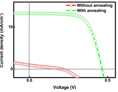
2.1.1 The effects of H
2annealing
The MIS solar cells exhibit poor photovoltaic characteristics without H2
annealing as shown in Fig.2.2 and Fig.2.3. The interface properties between the
ultrathin insulating layers and silicon wafers play an important role in the
performance of MIS solar cells.Large leakage current is observed in both C-V curves.
It indicates that there are probably a great number of trap states at the interface, such
as silicon dangling bonds (i.e., Si dangling bond interface states and suboxide species)
and silanol groups [15,16]. Charge carriers can flow via the trap states to cause
current leakage, and the capacitance is reduced.
To passivate those traps, H2 annealing was introduced. Fig. 2.2 to Fig. 2.5 show
the J-V and C-V curves of MIS solar cells with or without H2 annealling at 500℃ for
1 hour. The MIS solar cells with H2 annealing exhibit better photovoltaic properties.
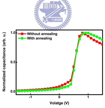
The C-V curves of the p-type and n-type MIS solar cells with H2 annealing display
smaller drops at the accumulation region. This can be attributed to the formation of
Si-H bonds at the interface. As a result, the trap states can be diminished, and the
leakage current is decreased. Therefore, H2 annealing can improve the performance of
MIS solar cells with ultrathin sputtering SiO2 layers because of the passivation of trap
13 0.0 0.5 0 10 Current dens it y ( m A/ cm 2 ) Voltage (V) Without annealing With annealing
Fig. 2.2: Photovoltaic properties of p-type MIS solar cell with and without H2
annealing. 0.0 0.5 0 10 Without annealing With annealing Cur rent density(mA/cm 2 ) Voltage (V)
Fig. 2.3: Photovoltaic properties of n-type MIS solar cell with and without H2
14 -2 -1 0 1 0.0 0.5 1.0 N o rm al iz ed ca pa ci ta nce ( arb . u. ) Voltage (V) Without annealing With annealing
Fig. 2.4: C-V measurement of p-type MIS solar cell with and without H2 annealing.
-1 0 1 0.0 0.5 1.0 N o rm al iz ed ca pa ci ta nce ( arb . u. ) Volatge (V) Without annealing With annealing
15
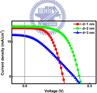
2.1.2 The effects of the thickness of SiO
2The thickness of insulating layer of MIS solar cells must be less than 2 nm so
that tunneling currents are sufficient for application. Fig. 2.6 and Fig. 2.7 show the
thickness of both p-type and n-type dependent J-V curves of MIS solar cells under
AM 1.5G with a SiO2 insulating layer deposited by RF sputtering. It is obvious that
not only Voc but also fill factor (FF) decreased with the increasing thickness of the
SiO2 insulating layer in the p-type MIS solar cells. An ultrathin insulating layer
sandwiched between metal and semiconductor can lower carrier recombination
probability and thus increases Voc, as shown in Fig. 2.6. But the tunneling probability
of minority carriers will be reduced significantly if the thickness of the insulating
layer is too thick. As a result, photo-excited carriers can not be collected by
electrodes.
Additionally, with increasing thickness, a voltage drop across the insulating layer
will also increase, and hence less output power can be used due to thermal dissipation.
Therefore, the thickness of the SiO2 insulating layer plays an important role in the
16 0.0 0.5 0 10 20 Cu rr ent densi ty ( m A /cm 2 ) Voltage (V) d~1nm d~2nm
Fig. 2.6: Thickness dependent J-V curves of p-type MIS solar cells.
0.0 0.5 0 10 Cu rr ent densi ty ( m A /cm 2 ) Voltage (V) d~1 nm d~2 nm d~3 nm
17
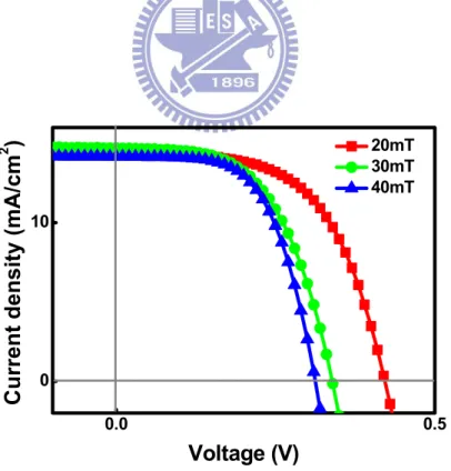
2.1.3 The effects of working pressure
The J-V curves of the MIS solar cells with the same thickness of ultrathin SiO2
deposited under different working pressures are shown in Fig. 2.8 and Fig. 2.9 for
p-type and n-type respectively. For the p-type MIS solar cells, the Voc values of
475mV, 386mV, and 350mV correspond to working pressures at 20mTorr, 30mTorr,
and 40mTorr, respectively. The Voc values of the n-type MIS solar cells are 422mV,
339mV, and 313mV corresponding to working pressures at 20mTorr, 30mTorr, and
40mTorr respectively. Higher working pressure results in lower Voc.
From C-V measurements as shown in Fig. 2.10 and Fig. 2.11, curve shift toward
positive bias (Fig.2.10) or negative (Fig. 2.11) with increasing working pressure
revealed that the barrier heights at MIS junctions are reduced. Furthermore, the slowly
capacitances rise at 30mTorr and 40mTorr marked by the yellow circles of working
pressure. Those indicated that more defects are induced in the ultrathin SiO2
insulating layers with increasing working pressure because of more plasma damages.
Therefore, the working pressure of RF magnetron sputtering affects on the barrier
18 0.0 0.5 0 10 20 Current densi ty (mA/cm 2 ) Voltage (V) 20mT 30mT 40mT
Fig. 2.8: The working pressure dependent J-V curves of p-type MIS solar cells.
0.0 0.5 0 10 Current densi ty (mA/cm 2 ) Voltage (V) 20mT 30mT 40mT
19 -2 -1 0 1 0.0 0.5 1.0 Nor m alize d ca pa cita nc e (ar b . u.)
Voltage (V)
20mT 30mT 40mTFig. 2.10: The working pressure dependent C-V curves of p-type MIS solar cells.
-1 0 1 2 0.0 0.5 1.0 Nor m alize d ca pa cita nc e (ar b . u.)
Voltage (V)
20mT 30mT 40mT20
2.2. Photovoltaic properties with different insulating layer
The key parameter of MIS solar cells is the insulating layer. In addition tosputtering ultrathin SiO2, the insulating layers are deposited by PECVD SiNx or
furnace SiOxNy for comparison. The ultrathin SiNx are deposited by PECVD at 300℃
by pyolysis of silane diluted in Ar (2% SiH4 in Ar) at a pressure of 100 pa and the rf
power at 35w. The ultra thin SiOxNy were deposited by quartz furnace at filling with
mixing gas oxygen and Nitrous oxide at 500℃.
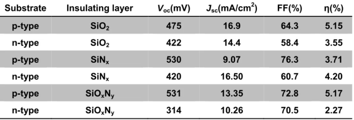
Table 2.1 lists the important properties of the MIS solar cells with a ultrathin
sputtering SiO2, PECVD SiNx, or thermal SiOxNy insulating layer. It is obvious that
the characteristics with a sputtering SiO2 insulating layer are comparable to those of
the others. If all MIS solar cells were deposited with a passivation layer(s), their
performance would been greatly promoted. This is because of the passivation layer(s)
can reduce surface recombination rate and the reflection of incident light. In addition,
the passivation layer(s) can provide positive or negative charges to induce inversion
layers near the surfaces.
From above results, sputtering SiO2 is an excellent alternative insulating layer of
MIS solar cells because of comparable characteristics of that using a PECVD SiNx or
thermal SiOxNy insulating layer and better thickness control.
21
Table 2.1: The key parameters of open circuit voltage, short circuit current
density, filling factor, energy conversion efficiency of the MIS solar cells with a
ultrathin sputtering SiO2, PECVD SiNx , or thermal SiOxNy insulating layer.
Substrate Insulating layer Voc(mV) Jsc(mA/cm2) FF(%) η(%)
p-type SiO2 475 16.9 64.3 5.15 n-type SiO2 422 14.4 58.4 3.55 p-type SiNx 530 9.07 76.3 3.71 n-type SiNx 420 16.50 60.7 4.20 p-type SiOxNy 531 13.35 72.8 5.17 n-type SiOxNy 314 10.26 70.5 2.27
The characteristics of MIS solar cells with sputtering a SiO2 insulating layer are
studied. Influences of the thickness of the SiO2 insulating layer and the working
pressure of the sputtering process are discussed. The thickness of the SiO2 insulating
layer has a great impact on tunneling probability of photo-excited minority carriers,
carrier recombination rate, and carrier collection efficiency. The working pressure of
RF magnetron sputtering has a significant impact on the barrier height and interface
defect density. The sputtering SiO2 is a good choice as a insulating layer of MIS solar
cells due to similar characteristics of that using a PECVD SiNx or thermal SiOxNy
insulating layer.
So far, the structure is front electrode / semi-transparent metal / insulating layer /
22
semi-transparent metal will be removed, textured surface will be formed, and then the
passivation layer will be deposited on top surface that will be discussed in the next
sections.
2.3. Surface texture
Optical and electrical losses are two major reasons that reduce the conversion
efficiency of silicon solar cells. Surface texturing is well known as one of the methods
to enhance the conversion efficiency of silicon solar cells by increasing the short
circuit current through effective light trapping. The textured surfaces of crystalline
silicon wafer are usually made in alkaline solutions. Alkaline etching of silicon, such
as potassium hydroxide (KOH) [20-22] and sodium hydroxide (NaOH) [17-19], is
anisotropic in nature, and therefore representative results of texturing for solar cell is
23
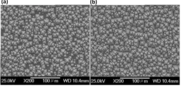
Fig. 2.12: SEM image of silicon surface with different etching time: (a) 30 minutes, (b)
40 minutes, (c) 50minutes, (d) 60minutes.
P-type silicon wafers (100) with a resistivity of 1-10 ohm-cmand n-type silicon
wafers (100) with a resistivity of 5-10 ohm-cm are used. First, after a standard RCA
cleaning process, the surfaces of the wafers are cleaned to remove any organic and
(a)
(b)
24
metal impurities. The wafers are dipped in buffed oxide etching (BOE) solution that
remove any unintentional oxide after rising the wafers with DI water between each
cleaning step. The cleaned wafers are texturized in alkaline etchants using mixtures of
potassium hydroxide (KOH) and isopropyl alcohol (IPA) at 85℃. There are five
duration times of texturing the surface: 0 minute (polish), 30 minutes, 40 minutes, 50
minutes and 60 minutes as shown in Fig. 2.12. The pyramids of all conditions are
7-10 μm in size. By comparison, the numbers of pyramids at texture time of 30
minutes obvious less and uneven distribution than others as shown in Fig. 2.12 (a).
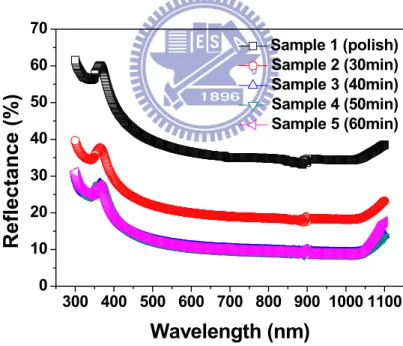
300 400 500 600 700 800 900 1000 1100 0 10 20 30 40 50 60 70
Refl
ectance (%)
Wavelength (nm)
Sample 1 (polish) Sample 2 (30min) Sample 3 (40min) Sample 4 (50min) Sample 5 (60min)Fig. 2.13: Reflectance of the textured silicon wafers for wavelength between 300 and
1100nm.
Fig. 2.13 shows the surface reflectance with different etching time at
25
non-textured wafer is higher than that of the textured wafers. In addition, the etching
time of wafer must exceed 30 minutes, and then, the reflection will close to saturation.
Fig. 2.14 provides a numerical comparison by averaging all of the reflectance values.
These results show that the etching time must exceed 30 minutes to obtain even
distribution and lower reflectance of pyramids.
Sample1 Sample2 Sample3 Sample4 Sample5 0 10 20
Aveag
e Refl
ect
an
ce (
%
)
Name of samplesFig. 2.14: Average % reflectance between 300and 1100nm.
2.4. Surface Passivation
Crystalline silicon is an indirect semiconductor and hence recombination losses
in the material occur largely via defect levels within the bandgap, notably at surface.
Due to the involvement of non-silicon atoms, the situation is more complicated at the
silicon surface. The surface represents the largest possible disturbance of the
39.15
21.90
26
symmetry of the crystal lattice and hence, because of non-saturated (‘dangling’) bonds,
a large density of defects (‘surface states’) within the bandgap exists at the surface of
the crystal [23]. 300 400 500 600 700 800 900 1000 1100 0 10 20 30 40 50 60 70
Refl
ectance (%)
Wavelength (nm)
Sample 1 (polish+SiNx 80nm) Sample 2 (30min+SiNx 80nm) Sample 3 (40min+SiNx 80nm) Sample 4 (50min+SiNx 80nm) Sample 5 (60min+SiNx 80nm)Fig. 2.15: Reflectance of the textured silicon wafers after anti-reflection coating
for wavelength between 300nm and 1100nm.
Because of high surface recombination losses and high surface reflectance, the
PECVD SiNx film is deposited on surface as highly efficient surface-passivating and
anti-reflection coatings [24-25]. The thickness of 80nm SiNx is deposited on above
substrates (There are five duration times of texturing the surface: 0 minute (polish), 30
27
with Fig. 2.11, the reflectance is reduced again. Fig. 2.16 provides a numerical
comparison by averaging all of the reflectance values. These results show that SiNx is
a good anti-reflection coating layer.
Sample1 Sample2 Sample3 Sample4 Sample5 0 10 20
Aveag
e Refl
ect
an
ce (
%
)
Name of samplesFig. 2.16: Average % reflectance between 300and 1100nm after depositing the
2.5
met dep Fig surf prop ther Fig. paas the enh5. Pho
In this sec tal is remo osited on to g. 2.17: The As shown face, the J-perties. From re are large . 2.20. It i sivation eff current den anced.otovoltai
ction, in ord oved, textur op surface a e structure o n in Fig. 2. -V curves w m the C-V c positive fix is obviousfect for the
nsity is imp
ic proper
der to obtain red surface as shown in of p-type M .18 with no with SiNx curve shift xed oxide ch that the Si MIS solar provement o 28rties of p
n more intro e is formed Fig. 2.17MIS solar cel
on-textured deposited a (from right harges with iNx film d cells. After outstandingl
p-type M
oduction of d, and then lls with text surface an at 100℃ d (Temp. 300 in the SiNx eposited at r the SiNx f ly but the oMIS solar
f light, the s n the passiture and pas
nd Fig. 2.19 display bett 0℃) to left layer at 10 t 100℃ can film is depo open circuit
r cells
emi-transpa ivation laye ssivation lay 9 with text ter photovo (Temp. 100 0℃as show n obtain b osited, not t voltage is arent er is yer. tured oltaic 0℃)), wn in etter only also29 -0.4 -0.2 0.0 0.2 0.4 0.6 0 10 20 30 40 50
Curren
t density (mA/cm
2)
Voltage (V)
no SiNx Temp. 100C Temp. 200C Temp. 300CFig. 2.18: Photovoltaic properties of MIS solar cells after depositing the SiNx
film with non-textured surfaces.
Table 2.2: Photovoltaic of MIS solar cells after depositing the SiNx film with
non-textured surfaces. Type Voc (mV) Jsc (mA/cm2) FF (%) η (%) No SiNx(non‐texture) 372 1.57 65.75 0.39 100 ℃(non‐texture) 533 37.07 34.26 6.77 200 ℃(non‐texture) 400 15.01 43.89 2.64 300 ℃(non‐texture) 393 11.28 48.16 2.14
The effects of the SiNx film deposited on the solar cell are ascribed to (i) the
reduction of the surface recombination velocity by hydrogen passivation of surface
states, (ii) the formation of an inversion layer at the silicon surface by the high
30 reflectance as shown in Fig2.15.
Table 2.2 and Table 2.3 summarize the one-sun parameters of the processed
p-type MIS solar cells featuring different surface passivation schemes, as measured
under standard testing conditions (25℃, 100mW/cm2, AM1.5G ). The results exhibit
significantly enhancement of a short circuit current of Jsc = 37.07mA/cm2, an open
circuit voltage of Voc = 533mV at the condition of 100℃(non-texture).
-0.4 -0.2 0.0 0.2 0.4 0.6 0 10 20 30 40 50
Curren
t density (mA/cm
2)
Voltage (V)
no SiNx Temp. 100C Temp. 200C Temp. 300CFig. 2.19: Photovoltaic properties of MIS solar cells after depositing the SiNx
31
Table 2.3: Photovoltaic of MIS solar cells after depositing the SiNx film with
textured surfaces. Type Voc (mV) Jsc (mA/cm2) FF (%) η (%) No SiNx (texture) 332 2.19 67.1 0.49 100 ℃(texture) 507 36.86 42.84 8.01 200 ℃(texture) 352 11.10 53.61 2.10 300 ℃(texture) 341 11.01 60.09 2.26 -40 -30 -20 -10 0 0.0 0.2 0.4 0.6 0.8 1.0 C / Cm ax Voltage (v) Temp. 300c Temp. 200c Temp. 100c
Fig. 2.20: The C-V curve of the SiNx film with different deposited temperatures.
2.6. Photovoltaic properties of n-type MIS solar cells
The device processes of n-type MIS solar cell are identical as p-type MIS solar
cells, except the thickness of SiO2. Although the SiNx film is an excellent passivtion
for p-type MIS solar cells, it is not suitable for n-type MIS solar cells. There are large
32
the p-type silicon underneath the SiNx. The benefits of the positive charges don’t meet
requirements of n-type MIS solar cells. Therefore, the Al2O3 film by e-gun
evaporation is substituted for SiNx because of the large amount of negative charges
within the Al2O3 film. We expect that using Al2O3 film can induce inversion layer for
n-type MIS solar cells applications.
-0.4 -0.2 0.0 0.2 0.4 0.6 -5 0 5 10 C u rrent densit y ( m A/cm 2 ) Voltage (V) Al2O3 (85nm) texture + Al2O3 (85nm)
Fig. 2.21: Photovoltaic properties of n-type MIS solar cells with Al2O3 films
As shown in Fig.2.21, although there are negative charges within Al2O3 film, the
effects of the Al2O3 film on n-type MIS solar cells are not significantly. From the
results, it is probably due to the Al2O3 film that is deposited by e-gun evaporating so
the quality of the Al2O3 film is worse compare with other deposition methods such as
ALD [27] and MOCVD. Therefore, the performances of n-type MIS don’t get
33 -0.4 -0.2 0.0 0.2 0.4 0.6 -5 0 5 10 15 20 25
Curren
t density (mA/cm
2)
Voltage (V)
Au 20nm texutre + Au 20nmFig. 2.22: Photovoltaic properties of n-type MIS solar cells with semi-transparent Au
Table 2.4: Photovoltaic of n-type MIS solar cells after depositing Al2O3 film or
semi-transparent Au Type Voc (mV) Jsc (mA/cm2) FF (%) η (%) Al2O3 240 0.3 41.14 0.03 Texture + Al2O3 381 6.21 45.49 1.08 Au 20nm 381 10.24 59.43 2.32 Texture + Au 20nm 380 19.76 58.42 4.39
Until now, we don’t find the useful passivation layer for n-type MIS solar cells
so semi-transparent Au of 20nm is re-deposited on textured surface. Fig. 2.22 shows
the J-V curve of n-type MIS solar cells with semi-transparent Au. The summary of the
34
2.7. Summary
In this chapter, using sputtering SiO2 as the insulating layer of MIS solar cells
has been discussed at different situations. The post annealing in hydrogen atmosphere
is necessary because there are a lot of defects in as-deposited sputtering SiO2.
Moreover, controlling the oxide thickness and working pressure are also critical in
MIS solar cells.
To concentrate more incident light, the semi-transparent metal is removed,
textured surface is formed, and then the passivation layer is deposited on top surface.
Finally, we use the textured surface and the 80nm SiNx films deposited at 100℃ as
passivation layer to reduce the surface reflection and the surface recombination. There
are exactly improvements in Voc and Jsc, but the fill factor is worse. So far, the Voc of
MIS solar cells can reach 507mV and 380mV for p-type and n-type on texture surface,
35
Chapter 3 MIS stacked solar cells
From the results of chapter 2, the n-type and p-type MIS solar cells are
demonstrated, and we use the direct wafer bonding method to combine n-type and
p-type in this chapter, then fabricate two MIS solar cells on both side each other. The
analysis of the MIS stacked show that the tunneling diode is formed between the
n-type and the p-type MIS solar cells, and the total thickness of MIS stacked solar
cells is critical.
3.1
Tunneling diode
Tunneling diode is also called Esaki diode [28-30] because it is invented by Leo
Esaki in August 1957. It is one of the most important issues affecting performance of
stacked solar cell. The effects of the formation of tunnel junction are related to the
uniform highly doped layer without defects that result in carrier recombination and
leakage currents in depletion regions. In a general tunneling diode, the degenerate
semiconductor [31,32] are used to increase tunneling probability via depletion region.
EF E kT ln N (Eq. 3.1) EC EF kT ln NC
(Eq. 3.2)
Nc and Nv are the effective density of states, n0 and p0 are doping density of the
with exh ohm app Fig diod the h n0 and p0 l As shown ibited whic mic phenom eared with i 3.1: Schem de with vary The curre I-V charact lager than N n in Fig. 3.1 ch is differe menon at sm increasing f matic energ ying bias [3 ent-voltage teristic and Nc and Nv. , the curren
ent from tra
mall voltage forward bia gy band dia 33]. characterist the band d 36 nt-voltage c aditional p-e, and nega s. agram and c tics of a tu diagram as haracteristi -n junction. ative differe current-volt unneling dio shown in F cs of a tunn The I-V cu ential resist tage proper ode can be Fig 3.2 and neling diode urve shows tance (NDR rty of tunne explained Fig.3.1. In e are s the R) is eling with n Fig
37
3.1(a), when a reverse bias is applied, current flows by electron tunneling from p–side
valence band which is occupied states into n-side conduction band which is
unoccupied states. In equilibrium, the net tunneling current is zero with no applied
bias in Fig 3.1(b). With a small forward bias, current flows by electron tunneling is
increased to a peak current Ip at voltage Vp, as labeled in Fig 3.1(c). When the position
of conduction band on the n-side is raised above the valence band position on the
p-side, the valley current Iv is resulted at a voltage Vv in Fig 3.1(d). With further
increasing in the voltage, the current increases due to tunneling through defect states
in the depletion layer and thermionic emission over the diode internal barrier, Fig
3.1(e).
For the better performance, the doping profile is key point for the performance in
a tunneling diode. Once an abrupt doping profile is obtained, the junction obtains the
lower resistance. That is, less voltage loss in a stacked solar cell with a higher Voc
could be acquired. On the contrary, the extended profiles of abrupt doping increases
the tunneling diode depletion region, and significantly reduces the tunneling
probability through depletion region. Accordingly, the performance of stacked solar
cell will be dramatically degraded.
Fig.3.2 shows a tunneling junction band diagram with ion implantation on polish
the bon
3.2
men than illum limi MIS curr doping pro nding [34-362
Fab
To realize ntioned in p n the skin mination. D ited by the S junction f rent matchi file of junct 6] to realize Fig. 3.2:brication
e a MIS stac preview sect depth of vi Due to the p bottom ce fabrication, ng in stack tion which e a better tun The band dn of MIS
cked solar c tions. 4-inc isible light, prospective ell which ge a thinning ked cells. C 38 is hardly co nneling junc diagram of tS stacked
cell, we sho ch Si wafers , so the bo of current m enerates les process of Chemical etc ontrol. Ther ction betwethe MIS stac
d solar ce
ould integra s has a thick ottom cell h matching, n ss current. bonded pai ching proce refore, we u en two MIS cked solar cells
ate three difkness about hardly abso net current o Consequen irs must be ess is propo use direct w S solar cells cell fferent junct t 525um thi orbs light u output woul ntly, before e done to ob osed to rem wafer s. tions icker under ld be two btain move
surf IPA proc face defect A, random p cesses are li (1) Wafer (2) Ion im p-side n-side (3) Wafer (4) Using (5) Direct in IPA (6) Heat u (7) Dopan Fig
and thin the
pyramid is isted below s are cleane mplantation w : Energy of : Energy of s are dipped acetone an t bonding of A and then pu up to 500℃ nts activated g. 3.3: Sche e wafer at t s formed o and show i ed by RCA c with dose 5 f implantatio f implantatio d in dilute H d IPA to cle f n-type and ut the bond and keep s d with rapid ematic top v 39 the same tim
on both sid in Fig. 3.2: clean. 5×10¹⁵ at the on are 24Ke on are 80Ke HF to remov ean by Ultra d p-type Si ded samples samples at 5 d thermal an
view and sid
me. Then, u des of the e polished s eV and10Ke eV and 20K ve native ox asonic clean wafers with into a clam 500℃ for 1 nnealing (RT de view of b using a solu stacked ce ide. eV. KeV. xide. ning. h polished s mp as shown 1 hour. TA) at 1050 bonding clam ution of KO ell. The d sides each o n in Fig. 3.3 0℃ for 10s mp H in detail other .
40
(8) Thinning wafers with Si etchant (HF:CH3COOH:HNO3=6:7:20) and
texturing wafers with other Si etchant (KOH:IPA:DI water =1:6:55).
(9) Wafers are cleaned by RCA clean.
(10) Deposit tunneling silicon dioxide with sputter at both sides.
(11) H2 annealing at 500℃ 1hr for passivating defects in silicon dioxide.
(12) The top cell deposits the semi-transparent and electrode Au fingers.
(13) The bottom cell deposits rear electrode Al.
(14) The structures of MIS stacked solar cells are shown in Fig. 3.3.
thic proc resp
3.3
poli befo caus bon den Fig. 3.5 ckness of se cess, the th pectively.3
Bon
In our exp ished, <100ore and afte
se of the bu nding surfac sity of bond shows the emi-transpar hickness of Fig. 3.5:
nding int
periments, a 0> oriented. er annealed ubbles form ce, (2) local ding species structure o rent Au. In f n-type an : Schematicterface b
all the bondAll of bon d because th m during the lized surfac s, and (4) tra 41 of the MIS order to ach nd p-type b c diagram of
by an IR
ded wafers nded wafer p he bubbles stacked cel ce protrusion apped air po S stacked s hieve curren become ab f MIS stackR CCD
are commepairs are ins
of bonding ll process in ns, (3) loca ockets [35]. solar cell w nt matching out 90μm
ked solar cel
ercially ava spected by g interface m nclude: (1) alized absen . with the 2 g, after thin m and 400μ lls
.
ailable, one infrared sys may occur. particles on nce of suffic 0nm nning μm, side stem The n the cienttran emp mat 1.12 crys into Step by a Because nsmitting li ployed, whe terial are us 2eV, only stalline silic o the imagin Fig 3.7 sh p C and Ste above descr Fig bonding w ight with a ere Eg is the sed. Accord the light w
con. The lig
ng system fo
hows that th
ep D, in Fig
ribe are app
. 3.6: Setup wafers are an appropr e smaller ba ding to Eq. with wavele ght bulb an or bonded S λ > Eg/
here are fou
g.3.5. We ca peared after 42 p of IR imag not transp iate wavele and gap am 3.3, since ength long nd an IR vie Si/Si pairs sh /h ur bonding an find that as-bonded ge measurem parent to n ength base
mong the bon
crystalline ger than 1. ewing came hown in Fig (Eq. 3 interface im some certa process in ment normal vis d on Eq. nding mater silicon ban 10μm can
era are used
g. 3.7 3.3) mages, as S ain voids wh Step A. Ste sible light, 3.3 has to rials if diffe ndgap energ n pass thro d to investi Step A, Ste hich may c ep B, With the o be erent gy is ough igate p B, ause RTA
43
1050℃, the outgassing develops from contaminants on inside bonding materials due
to the a heat treatment. Then, Step C, because of RCA clean at 90℃, the gases are
diffused along the bonding interface. Finally, when bonded pairs thinning and textured
by using silicon etchant, the image don’t change obviously because the Step D
process temperature of the step D (85℃) is close to Step C.
From the results, if there are a lot of bubbles formed at as-bonded, the bonded
Si/Si pairs will easily separate after post processes.
44
3.4
Photovoltaic properties of MIS stacked solar cells
The current-voltage curves of MIS stacked solar cells under AM1.5 are shown inFig. 3.8 and Table 3.1. All parameters of the device process are identical unless with
or without semi-transparent metal. The cell is thinning as above describe, the
thickness of n-type and p-type are about 90μm and 400μm, respectively. From the
currents of Fig 3.8, Jsc is low about 5.9mA/cm2 despite with or without
semi-transparent metal. -0.4 -0.2 0.0 0.2 0.4 0.6 0.8 0 2 4 6 8
C
u
rr
e
n
t density (mA
/cm
2)
Voltage (V)
no semi-transparent Au Au 20nmFig. 3.8 Photovoltaic properties of MIS stacked solar cells with or without
45
Table 3.1 Photovoltaic properties of MIS stacked solar cells with and without
semi-transparent metal.
Through the incident photon to current efficiency (IPCE) curves as shown in Fig.
3.9, we can realize Jsc by IPCE measurement system are higher than solar simulator
measurement system, and the currents with semi-transparent metal cell are larger than
without semi-transparent metal cell. In Table 3.2, The semi-transparent metal improve
the currents of IPCE measurement but the currents have no enhancement of solar
simulator measurement systems which ascribe to limited current by the bottom cell.
Table 3.2: The current density is measured by different measurements (solar simulator
46 300 450 600 750 900 1050 0 10 20 30 40 50
IPCE (%)
Wavelength no semi-transparent Au Au 20nmFig. 3.9: IPCE curves of MIS stacked solar cells with and without semi-transparent
metal. 300 400 500 600 700 800 900 1000 1100 1200 0 3 6 9 12 15 T ran smi s si on ( % ) Wavelength n-type(~90um) p-type(~400um)
47
However, we can realize that the transmission of the thickness 90μm of n-type
silicon increase drastically after an appropriate 900nm of wavelength from the Fig.
3.10. It means that the bottom cell would absorb infrared light not the visible light so
the photo currents of bottom cell would be small.
3.5
Summary
The tunneling diode is fabricated by direct bonding method with ion
implantation on polish side each other. Dopants are activated by RTA at 1050℃. In
order to get current matching, the thickness of devises has to thinning by silicon
etchants. Although the total thickness are reduced to 490μm, the device are not
transparent to normal visible light, the transmitting light with an appropriate
wavelength is 900nm. The bottom cell absorbs too less light, so products a little
current. Finally, we integrate the n-type and the p-type to form a MIS stacked solar
cell which can obtain Voc=720mV, Jsc=5.96mA/cm2, FF= 58.96%, η= 5.93. The Voc
of MIS stacked cells obtain 720mV which is larger than that of p-type and n-type
48
Chapter 4 Conclusion and future work
4.1 Conclusion
In this study, first, the characteristics of both p-type and n-type
Metal-Insulator-Semiconductor (MIS) solar cells with sputtering SiO2 insulating
layers fabricated by radio-frequency (RF) magnetron sputtering are investigated
individually.
From the beginning, the structure of the MIS solar cell is proposed with the
semi-transparent metal on both n-type and p-type silicon substrates. The influence of
processes parameters are researched such as H2 annealing, insulating layer thickness
and the working pressure on the MIS solar cell. However, the reflection of surface is
high due to the semi-transparent metal. In order to reduce the reflection of surface, we
remove the semi-transparent metal, form the texture on surface, and then deposit the
passivating SiNx film on surface as a AR coating which also can induce the inversion
layer on the insulating layer between metal and semiconductor so that improve the
performance of the p-type MIS solar cells. Regarding the n-type MIS solar cells, we
also deposit Al2O3 film as the passivating layer, but the effects on n-type MIS solar
cell are not obviously. Therefore, the structure of n-type MIS solar cells with the
semi-transparent metal are used to make the MIS stacked solar cell. So far, MIS solar
49
Finally, by the direct wafer bonding, we integrate the n-type and the p-type to
form a MIS stacked solar cell which can obtain Voc=720mV, Jsc=5.96mA/cm2, FF=
58.96%, η= 5.93. The Voc of MIS stacked cells obtain 720mV which is larger than
that of p-type and n-type cells.
4.2 Future work
Although the Voc on the MIS stacked solar cell is 720mV which is lower than
theoretic Voc equals to 0.9V. There are still many issues that exist in the staked cell.
The voltage drops at the bonding interfaces that can further improve by the tunneling
current with proper dopants activation and defect passivation. However, the total
thickness of MIS stacked solar cell is another important issue. In order to obtain the
current matching, the bottom cell needs to absorb more sunlight. Therefore, the total
thickness has to be decreased and optimized.
In addition to the issues of the bonding interface and thickness, we can use
different substrate to bond together such as Ge substrate, or deposit different bandgap
Si such as uc-Si so that in order to absorb different region sunlight. Although the
semi-transparent metal has been removed, the finger electrodes also reflect the
sunlight. The transparent conductive oxide such as ITO and ZnO can be introduced in
50
References
[1] Zhores I. Alferov, V. M. Andreev, M. B. Kagan, I. I. Protasov,and V. G. Trofim,
Fiz. Tekh. Poluprovodn, Vol.4 ,p.2378 (1970)
[2] Zhores I. Alferov, Rev. Mod. Phys., Vol.73, p.767 (2001)
[3] R. Hezel, Prog. PV Res. Appl. ,Vol.5, p.109 (1997)
[4] R. Hezel, Solid State Electron., Vol.24, p.863 (1981)
[5] R. Hezel and R. Schorner, J. Appl. Phys., Vol.52, p.3076 (1981).
[6] R. Schorner and R. Hezel, IEEE Trans. Electron. Devices, ED-28, p.1466 (1981)
[7] R. Hezel, Conf. Rec. 16th IEEE Photovoltaic Specialists Conf., San Diego,
p.1237 (1982)
[8] K. Jaeger and R. Hezel, IEEE Trans. Electron. Devices, ED-32, p.1824 (1985)
[9] R. Hezel, W. Hoffmann and K. Jaeger, Proc. 10th European Photovoltaic Solar
Energy Conf., Lisbon, p. 511 (1991)
[10] A Metz, R Meyer, B Kuhlmann, M Grauvogl and R Hezel , Proceedings of the
26th IEEE PVSC, p.31 (1997)
[11] Kuo-Chung Lee and Jenn-Gwo Hwu, IEEE Electron Device Lett., Vol.18, p.565
(1997)
[12] Chih-Yao Wang and Jenn-Gwo Hwu, J. Electrochem. Soc., Vol.156, p.3 (2009)
51 p.69 (1996)
[14] Armin G. Aberle and Rodolf Hezel, Prog. Photovoltaics., Vol.5, p.29 (1997)
[15] A. Hartstein and D. R. Youn, Appl. Phys Lett., Vol.38, p.631 ()
[16] Asuha, Y-L Liu, O. Maida, M. Takahashi, and H. Kobayashi, J. Electrochem.
Soc., Vol.151, p.G824 (2004)
[17] P.K. Singh, R. Kumar, M. Lal, S.N. Singh, B.K. Das, Sol. Energy Mater. Sol.,
Vol.70, p.103 (2001)
[18] E. Vazsonyi, K. De Clercq, R. Einhaus, E. Van Kerschaver, K. Said, J. Poortmans,
J. Szlufcik, J. Nijs, Sol. Energy Mater. Sol., Vol.57, p.179 (1999)
[19] Zhenqiang Xi, Deren Yang, Wu Dan, Chen Jun, Xianhang Li, Duanlin Que,
Renew. Energy, Vol.29, p.2101 (2004)
[20] Hayashi Shota, Minnemoto Takashi, Takakura Hideyuki, Hamakawa Yoshihiro,
Rare Metals, Vol.25, p.115 (2006)
[21] David L. King, M. Elaine Buck, p303 IEEE (1991)
[22] J.W. Faust Jr., E.D. Palik, J. Electrochem. Soc., Vol.130, p.1413 (1983)
[23] Armin G. Aberle, Prog. Photovoltaics., Vol.8, p.473 (2000)
[24] Hayoung Park, Soonwoo Kwon, Joon Sung Lee, Hee Jin Lim, Sewang Yoo and
Donghwan Kim, Sol. Energy Mater. Sol., Vol.93, p.1773 (2009)
52 Kim, Curr. Appl. Phy., Vol.10, p.113 (2010)
[26] E.P. Burte and R.Hezel, J. Appl. Phys., Vol.55, p.4 (1984)
[27] J.Schmidt, A.Merkle, R. Brendel, B. Hoex, M. C. M. van de Sanden and W. M.
Kessels, Prog. Photovolt: Res. Appl., Vol.16, p.461 (2008)
[28] L. Esaki, Phys. Rev., Vol.109, p.603 (1958)
[29] L. Esaki, Proc. IEEE, Vol.62, p.825 (1974)
[30] L. Esaki, IEEE Transactions on Electron Devices, Vol. ED-23, p.644 (1976)
[31] S. M. Sze, “Physics of Semiconductor Devices” 2nd Ed. (Wiley, New York,
1981)
[32] DA Neamen, “Semiconductor Physics and Devices” 3rd Ed. (McGraw-Hill, New
York,2003)
[33] Y Yan, “SILICON-BASED TUNNEL DIODE TECHNOLOGY”
[34] Xuan Xiong Zhang and Jean-Pierre Raskin, J. Microelectromech. Syst., Vol.14
p.2 (2005)
[35] Q-Y. Tong and U.Gosele, “Semiconductor Wafer Bonding: Science and
Technology ”
[36] Seiji Fujino, Masaki Matsui, Tadashi Hattori and Yoshihiro Hamakawa, Jap. J.
![Fig. 1.2: A truncated-pyramid MIS-IL silicon solar cell [13].](https://thumb-ap.123doks.com/thumbv2/9libinfo/8230731.170899/15.892.261.687.126.470/fig-truncated-pyramid-mis-silicon-solar-cell.webp)