國
立
交
通
大
學
電子工程學系電子研究所碩士班
碩 士 論 文
利用金屬嵌入層提升溶膠凝膠法製備之
鈦酸鉍薄膜電阻轉態特性
Modification of Resistive Switching Characteristics
in Sol-Gel Derived Bi
4Ti
3O
12Thin Film
Using Embedded Metal
研 究 生:黃毅函
指導教授:曾俊元 教授
利用金屬嵌入層提升溶膠凝膠法製備之鈦酸鉍薄膜
電阻轉態特性
Modification of Resistive Switching Characteristics in Sol-Gel
Derived Bi
4Ti
3O
12Thin Film Using Embedded Metal
研 究 生:黃毅函
Student
:Yi-Han Huang
指導教授: 曾俊元 教授 Advisor : Prof.
Tseung-Yuen Tseng
國 立 交 通 大 學
電子工程學系電子研究所碩士班
碩 士 論 文
A Thesis
Submitted to Department of Electronics Engineering and Institute of Electronics
College of Electrical and Computer Engineering
National Chiao-Tung University
in Partial Fulfillment of the Requirements
for the Degree of Master
in Electronic Engineering
July 2008
Hsinchu, Taiwan, Republic of China
利用金屬嵌入層提升溶膠凝膠法製備之鈦酸鉍薄膜電阻轉態特性
研究生:黃毅函 指導教授:曾俊元
國立交通大學
電子工程學系電子研究所
摘要
近來新世代非揮發性記憶元件受到廣泛的注意,諸如相變化記憶體、磁阻式記憶 體、鐵電記憶體、電阻式記憶體等。其中又以電阻式記憶元件最受囑目,由於其具有低 操作電壓、結構簡單、讀寫速度快、低耗能、非破壞讀取等優點,將有助於達到高密度 積體整合及低操作功率的目的,因此可以期待電阻式記憶體成為未來非揮發性記憶體的 主流。 本論文選用層狀鈣鈦礦結構材料(鈦酸鉍)作為電阻式記憶體的轉態層材料,利用 溶膠凝膠法製備鈦酸鉍薄膜,並且首次在薄膜中間嵌入兩奈米厚度的鉻金屬層來改善轉 態特性,而此結構的轉態層厚度約為二十二奈米。本論文著重在於如何降低並穩定操作 電壓,除了嵌入鉻金屬外,更利用後續高溫退火步驟來實現。結果發現退火 600 度下, 擁有最低的操作電壓(約為-2 伏特),而且,在記憶測試中,例如:耐久度、非破壞讀取、 儲存能力等都擁有極佳的表現度。本實驗更利用材料分析結果去驗證電性表現,並探討 嵌入金屬層對於轉態層的影響。隨後我們也探討電壓電流關係,去探討可能的電阻式記 憶體的電阻轉換特性及傳導機制。Modification of Resistive Switching Characteristics in Sol-Gel
Derived Bi
4Ti
3O
12Thin Film Using Embedded Metal
Student: Yi-Han Huang
Advisor: Tseung-Yuen Tseng
Department of Electronics Engineering and Institute of Electronics
National Chiao Tung University
Abstract
In recent year, next-generation nonvolatile memories (NVM), such as OUM, MRAM, FRAM and RRAM, have attracted a lot of attention because of its ascendant advantages such as simple device structure, low operation voltage, low power consumption, long retention time, small cell size, high operation speed, low cost, good endurance, and non-destructive readout, which help for attaining to objects of high density integration and low power operation.
In this thesis, the RRAM devices manufactured based on Sol-Gel derived Bi4Ti3O12 thin
films are studied and developed. The electrical properties are enhanced by using embedded 2nm-Cr in BTO thin film. The thickness of switching oxide is about 22nanometer. The main point is accented on how to decrease and stabilize the operation voltage. Except using embedded metal, thermal treatment like post deposition annealing is used as well. Accidentally, the lowest operation voltage (-2V) appears at the condition with annealing at 600oC. Also, in memory test such as endurance, retention and voltage stress, the device shows the best performance. The material analyses are applied to verify the electrical phenomenon. In addition, the related conduction mechanism is discussed in detail.
誌謝
首先,要感謝我的指導老師曾俊元教授在我兩年的研究生生涯裡,提供如此良好的 實驗室環境,並在專業領域上給予我許多的建議,使我能順利完成本篇論文。此外,也 要感謝國家毫微米實驗室、清大貴重儀器中心、交大貴重儀器中心等單位,提供良好的 研究環境讓我完成實驗。也特別感謝林晨曦博士以及林昭吟博士對本論文的建議,使論 文內容更趨完善。 其次,謝謝林群傑學長、林志洋學長,在我實驗、課業以及論文上總是給予我很多 實驗內容的建議。而林孟漢學長、吳明錡學長在實驗上更是給我很大的幫助,使我的論 文內容更佳的完備,沒有你們的協助,我很難這麼順利畢業。也要感謝姚奕全、王聖裕、 李岱螢這幾位學長在實驗細節上也提供了不少的寶貴意見,以及另外還有莊文仁、詹世 偉、翁啟翔、顏宏全這幾位同學,很感謝有你們這兩年陪伴,使得我兩年的研究生活中 增添了許多歡樂,而且也在實驗及課業上幫了我不少,我會好好珍惜這一份難得的友 誼。李盈賢、葉昱廷、蔡承翰、孫淑炫、黃志文這幾位學弟妹,多謝你們在實驗上的幫 忙。還有曾給予我協助的朋友,若沒有你們,我也不會這麼順利。也感謝女朋友旻諭這 兩年的陪伴,讓我過了一段美好的研究生活。 最後還要感謝我的爸爸媽媽,很感謝你們竭盡全力的支持我讀研究所,讓我無後顧 之憂能順利完成研究所學業,在此,將這份論文獻給你們。Contents
Chinese Abstract ………. i
English Abstract ……….. ii
Acknowledgement……….………….. iii
Contents ………... iv
Table Captions ………. viii
Figure Captions ………... ix
Chapter 1 Introduction 1.1 Memories Classification ………... 1
1.2 Conventional Nonvolatile Memory ………...…... 1
1.2.1 Read Only Memory ………... 2
1.2.2 Programmable Read Only Memory ………...…….... 2
1.2.3 Mask-Programmed Read Only Memory ……….... 3
1.2.4 Erasable and Programmable Read Only Memory ……….. 3
1.2.5 Ultraviolet-Erase EPROM ………. 3
1.2.6 One-Time Programmable (OTP) Read Only Memory………... 1.2.7 Electrically Erasable and Programmable Read Only Memory………... 1.2.8 Flash Memory………... 4 4 4 1.3 Promising Next-Generation Nonvolatile Memory ………... 6
1.3.1 Ovonic Unified Memory ………...…………...…………... 6
1.3.2 Magnetic Random Access Memory………... 6
1.3.3 Ferroelectric Random Access Memory ………. 8
1.3.4 Resistance Random Access Memory ………... 10
1.4.1 Metal-Insulator-Metal Structure………. 1.4.2 Operation Method……….. 1.4.3 Introduction to Perovskite materials……….. 1.4.4 Resistive Switching Mechanisms……….. 1.5 Important Criteria for RRAM………...
10 11 11 12 16
Chapter 2 Experiment Details 23
2.1 Experimental Process Flow ……….. 23
2.2 Sample Preparation………... 24
2.2.1 RCA Cleaning of Silicon Substrate ………... 24
2.2.2. Furnace Oxidation of Silicon Substrate……… 24
2.2.3. Deposition of Bottom Electrode………... 25
2.2.4. Deposition of LaNiO3 Thin Films………. 25
2.2.5. Rapid Thermal Annealing Process of LaNiO3 Thin Films……… 25
2.2.6. Deposition of Bi4Ti3O12 Thin Films……….. 2.2.7. Post Deposition Annealing Process of Bi4Ti3O12 Thin Films……….... 2.2.8. Deposition of Top Electrode……….. 26 26 27 2.3 Electrical Measurement and Material Analyses………. 27
2.3.1 Current-Voltage (I-V) Measurement………... 27
2.3.2 X-Ray Diffraction………... 28
2.3.3 Atomic Force Microscopy ……….. 28 2.3.4 Scanning Electron Microscopy ………..
2.3.5 Transmission Electron Microscopy………. 2.3.6 Secondary Ion Mass Spectrometer……….
29 29 29
Chapter 3 Results and Discussion
3.1 Pure BTO thin film ……….... 34
3.1.1 Thickness of pure BTO thin film……….... 34
3.1.2 Forming process……….. 35
3.1.3 Operation mode and voltage………... 35
3.1.4 Memory test for endurance………. 36
3.1.5 Thermal effect of post deposition annealing………... 36
3.1.6 Summary for thinner pure BTO thin film………... 36
3.2 The effect of embedded metal in BTO thin film……… 37
3.2.1 Materials for embedded metal………. 37
3.2.2 The effect of thermal treatment………... 37
3.2.3 Resistive switching properties of embedded Cr BTO thin film……….. 38
3.3 Physical property analyses of 2nm Cr embedded……….. 39
3.3.1 X-Ray Diffraction………... 39
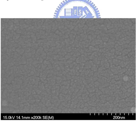
3.3.2 Scanning Electron Microscope………... 39
3.3.3 Atomic Force Microscope………... ……… 40
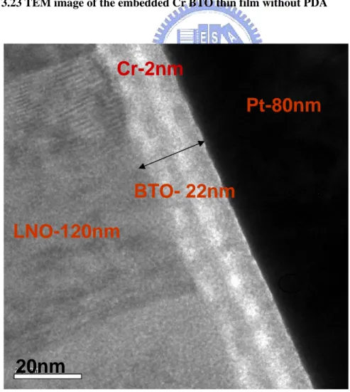
3.3.4 Transmission Electron Microscope……….. 40
3.4 Electrical Property Analyses of 2nm Cr Embedded……… 41
3.4.1 Resistive Switching Characteristics……… 41
3.4.2 Memory Test………... 42
3.4.3 Curve Fitting of Current-Voltage Plots………... 43
3.4.4 The relation between temperature and current……… 44
3.4.5 Possible mechanism……… 45
3.5 Electrical Property Analyses for 2nm Pt Embedded……… 45
3.5.2 Curve Fitting of Current-Voltage Plots………... 46 3.5.3 The relation between temperature and current……… 47
3.5.4 Possible mechanism……… 47
Chapter 4 Conclusions
4.1Conclusions ………. 83
Figure Captions
Chapter 1
Figure 1.1 A schematic of an MTJ memory cell. Arrows indicate possible directions of
magnetic movement………... 19
Figure 1.2 MRAM array………. 19
Figure 1.3 Hysteresis loop of FRAM cell capacitor……… 20
Figure 1.4 RRAM consists of a transistor and a resistor. The transistor is fabricated in the front end and the resistor in the back end……… 20
Figure 1.5 Schematic view of stacked memory layers. The cell sizes decrease from 4F2 to 4F2/n for n layers……… 21
Figure 1.6 Equivalent circuit of an array for the write operation of a given bit resistor………... 21
Figure 1.7 Equivalent circuit of an array for the reset operation of a given bit resistor………. 22
Figure 1.8 Perovskite structure. The red spheres are oxygen atoms, the deep blue are smaller metal cations and the green/blue are the larger metal cations………. 22
Chapter 2 Figure 2.1 The illustration of the experiment flow……… 30
Figure 2.2 The cross section view of conventional BTO structure……… 31
Figure 2.3 The cross section view of modified BTO structure……….. 31
Figure 2.4 The illustration of the sample preparation flow……… 32
Chapter 3
Figure 3.1 The forming curve and first cycle of pure BTO thin film without PDA…….. 48
Figure 3.2 Endurance of pure BTO thin film without PDA………... 48
Figure 3.3 Electrical properties of 10nm Cr embedded BTO thin film without PDA….. 49
Figure 3.4 Electrical properties of 10nm Cr embedded BTO thin film with PDA 500oC. 49 Figure 3.5 Electrical properties of 10nm Cr embedded BTO thin film with PDA 600oC. 50 Figure 3.6 Electrical properties of 10nm Cr embedded BTO thin film with PDA 700oC. 50 Figure 3.7 Electrical properties of 5nm Cr embedded BTO thin film without PDA…… 51
Figure 3.8 Electrical properties of 5nm Cr embedded BTO thin film with 500oC PDA... 51 Figure 3.9 Electrical properties of 5nm Cr embedded BTO thin film with 600oC PDA... 52 Figure 3.10 Electrical properties of 5nm Cr embedded BTO thin film with 700oC PDA... 52 Figure 3.11 Forming process of various Cr thicknesses in the embedded BTO thin film… 53
Figure 3.12 Resistive switching I-V curves of various Cr thicknesses in the embedded
BTO thin film……… 53
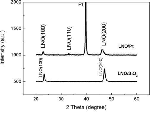
Figure 3.13 XRD pattern of LNO/Pt and LNO/SiO2 bottom electrode………... 54
Figure 3.14 XRD pattern of embedded Cr BTO thin film with different thermal
treatment……… 54
Figure 3.15 Top view SEM images of embedded Cr BTO thin film without PDA………. 55
Figure 3.16 Top view SEM images of embedded Cr BTO thin film with PDA 500oC…… 55 Figure 3.17 Top view SEM images of embedded Cr BTO thin film with PDA 600oC…… 56 Figure 3.18 Top view SEM images of embedded Cr BTO thin film with PDA 700oC…… 56 Figure 3.19 2D and 3D AFM image of the embedded Cr BTO thin film without PDA….. 57
Figure 3.20 2D and 3D AFM image of the embedded Cr BTO thin film with PDA 500oC. 58 Figure 3.21 2D and 3D AFM image of the embedded Cr BTO thin film with PDA 600oC. 59 Figure 3.22 2D and 3D AFM image of the embedded Cr BTO thin film with PDA 700oC. 60 Figure 3.23 TEM image of the embedded Cr BTO thin film without PDA………. 61
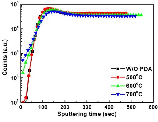
Figure 3.25 SIMS for proving the La diffusion of bottom electrode LNO 62
Figure 3.26 The statistics for forming voltage of different annealing temperatures……… 62
Figure 3.27 Forming I-V curves of different annealing temperatures……….. 63
Figure 3.28 Switching I-V curves of different annealing temperatures………... 63
Figure 3.29 Statistics of operation voltage with different annealing temperatures………. 64
Figure 3.30 The statistics of ON and OFF state resistance with different annealing temperatures……….. 64
Figure 3.31 Accumulative plots for turn-on and turn-off voltage……… 65
Figure 3.32 Switching cycles of embedded 2nm-Cr device without PDA……….. 65
Figure 3.33 Switching cycles of embedded 2nm-Cr device with PDA 500oC……… 66
Figure 3.34 Switching cycles of embedded 2nm-Cr device with PDA 600oC………. 66
Figure 3.35 Switching cycles of embedded 2nm-Cr device with PDA 700oC………. 67
Figure 3.36 Write/Erase cycles test for ON-State and OFF-state of sample without PDA.. 67
Figure 3.37 Write/Erase cycles test for ON-State and OFF-state of sample with PDA 500oC………. 68
Figure 3.38 Write/Erase cycles test for ON-State and OFF-state of sample with PDA 600oC………. 68
Figure 3.39 Write/Erase cycles test for ON-State and OFF-state of sample with PDA 700oC………. 69
Figure 3.40 Endurance comparisons of different devices……… 69
Figure 3.41 Retention test at room temperature of embedded 2nm-Cr with PDA 600 o C device……… 70
Figure 3.42 Retention test at 85oC of embedded 2nm-Cr with PDA 600oC device………. 70
Figure 3.43 Voltage stress at room temperature of embedded 2nm-Cr with PDA 600oC device……… 71
Figure 3.44 Voltage stress at 85oC of embedded 2nm-Cr with PDA 600oC device………. 71
Figure 3.45 Curve fitting at positive bias region for embedded 2nm-Cr device without PDA………... 72
Figure 3.46 Curve fitting at negative bias region for embedded 2nm-Cr device without PDA………... 72
Figure 3.47 Curve fitting at positive bias region for embedded 2nm-Cr device with PDA
600oC………. 73
Figure 3.48 Curve fitting at negative bias region for embedded 2nm-Cr device with PDA 600oC………. 73
Figure 3.49 ON-State conductivity of measurement at various temperatures……….. 74
Figure 3.50 OFF-State conductivity of measurement at various temperatures……… 74
Figure 3.51 The activation energy of ON and OFF states……… 75
Figure 3.52 Electrical property of embedded 2nm-Pt device without PDA………. 75
Figure 3.53 Electrical property of embedded 2nm-Pt device with PDA 500oC…………... 76
Figure 3.54 Electrical property of embedded 2nm-Pt device with PDA 600oC…………... 76
Figure 3.55 Electrical property of embedded 2nm-Pt device with PDA 700oC…………... 77
Figure 3.56 Statistics for resistance of ON-State and OFF-State at various temperatures... 77
Figure 3.57 Curve fitting at positive bias region for embedded 2nm-Pt device without PDA………... 78
Figure 3.58 Curve fitting at negative bias region for embedded 2nm-Pt device without PDA………... 78
Figure 3.59 Curve fitting at positive bias region for embedded 2nm-Pt device with PDA 600oC……….. 79
Figure 3.60 Curve fitting at negative bias region for embedded 2nm-Cr device with PDA 600oC……….. 79
Figure 3.61 ON-State conductivity of measurement at various temperatures for embedded 2nm-Pt device with PDA 600oC………... 80
Figure 3.62 OFF-State conductivity of measurement at various temperatures for embedded 2nm-Pt device with PDA 600oC………... 80
Figure 3.63 SIMS for proving the Pt diffusion in BTO thin film………. 81
Figure 3.64 Illustrations of conduction mechanism in embedded 2nm-Pt devices… 81 Figure 3.65 Comparison in device yield………. 82
Chapter 1
Introduction
1.1 Memories Classification
In this chapter, many kinds of memories are introduced generally. Basically, memories can be divided into two opposing categories: volatile and nonvolatile memory. In each category, there will be several kinds of memories. In this thesis, however, I would like to focus on the nonvolatile memory (NVM) and give a roughly introduction about each kind of NVMs.
1.2 Conventional Nonvolatile Memory
In 1967, D. Kahng and S. M. Sze proposed the first floating gate nonvolatile memory [1]. In recent year, NVM has been widely used in the portable devices, such as flash memory device, cell phone, digital camera, mp3 players, and personal digital assistant. Nonvolatile memory is typically used for the task of secondary storage, or long term persistent storage. The most widely used form of primary storage today is a volatile form of random access memory (RAM), meaning that when the computer is shut down, anything contained in RAM is lost. Unfortunately, most forms of nonvolatile memory have limitations that make them unsuitable for use as primary storage. Typically, nonvolatile memory either costs more or performs worse than volatile random access memory. Nonvolatile data storage can be categorized in electrically addressed systems random access memory and mechanically addressed systems hard disks, optical disc and magnetic tape. Electrically addressed systems are expensive, but fast, whereas mechanically addressed systems have a low price per bit, but are slow. Nonvolatile memory may one day eliminate the need for comparatively
slow forms of secondary storage systems, like hard disks.
Following the popularity of mobile equipments, nonvolatile memory plays an important role in the electronic industries. The nonvolatile memory should keep the stored information without power supply for a long time. [2-3]
1.2.1 Read Only Memory
The very first ROMs are hardwired devices that contain a preprogrammed set of data or instructions. The contents of the ROM have to be specified before chip production, so the actual data can be used to arrange the transistors inside the chip. Hardwired memories are still used, though they are now called masked ROMs to distinguish them from other types of ROM. The primary advantage of a masked ROM is its low production cost. Unfortunately, the cost is low only when large quantities of the same ROM are required.
1.2.2 Programmable Read Only Memory
One step up from the masked ROM is the PROM, which is purchased in an undetermined state. If you look at the contents of an undetermined PROM, you would see that the data is made up entirely of 1's. The process of writing your data to the PROM involves a special piece of equipment called a device programmer. The device programmer writes data to the device one word at a time by applying an electrical charge to the input pins of the chip. Once a PROM has been programmed in this way, its contents can never be changed. If the code or data stored in the PROM must be changed, the current device must be discarded. As a result, PROMs are also known as one-time programmable devices.
1.2.3 Mask-Programmed Read Only Memory
One of the earliest forms of nonvolatile read only memory, the
mask-programmed read only memory was rewired at the design stage to contain specific data. Once the mask was used to manufacture the integrated circuits, the data was cast in stone and could not be changed. Whatever 1s and 0s were in memory, it left the factory there for life. The mask read only memory was therefore useful only for large-volume production, such as for read only memories containing the startup code in early microcomputers.
1.2.4 Erasable and Programmable Read Only Memory
An EPROM is programmed in exactly the same manner as a PROM. However, EPROMs can be erased and reprogrammed repeatedly. To erase an EPROM, you simply expose the device to a strong source of ultraviolet light. (A window in the top of the device allows the light to reach the silicon.) By doing this, it is practically to reset the entire chip to its initial-undetermined-state. Though more expensive than PROMs, their ability to be reprogrammed makes EPROMs an essential part of the software development and testing process.
1.2.5 Ultraviolet-Erase EPROM
The original erasable nonvolatile memories were EPROM’s; these could be
readily identified by the distinctive quartz window in the centre of the chip package. These operated bt trapping an electrical charge on the gate of a filed effect transistor in order to change a 1 to 0 in memory. To remove the charge, one would place the chip under an intense short wavelength fluorescent ultraviolet lamp for 20-30 minutes, returning the entire chip to its original blank state.
1.2.6 One-Time Programmable (OTP) Read Only Memory
An OTP is electrically an EPROM, but with the quartz window physically
missing. Like the fuse PROM it can be written once, but cannot be erased. It has largely replaced PROM chips in electronic production as an EPROM with no window is inexpensive to manufacture and can e programmed using identical equipment to that used to write to the UV-window EPROM.
1.2.7 Electrically Erasable and Programmable Read Only Memory
EEPROMs are electrically-erasable-and-programmable. Internally, they are similar to EPROMs, but the erase operation is accomplished electrically, rather than by exposure to ultraviolet light. Any byte within an EEPROM may be erased and rewritten. Once EEPROM is written the new data, the new data will remain in the device forever or at least until it is electrically erased. The primary tradeoff for this improved functionality is higher cost, though write cycles are also significantly longer than writes to a RAM. So EEPROM is used for main system memory.
1.2.8 Flash Memory
Flash memory [4-6] is non-volatile computer memory that can be electrically erased and reprogrammed. It is a technology that is primarily used in memory cards and USB flash drives for general storage and transfer of data between computers and other digital products. It is a specific type of EEPROM (Electrically Erasable Programmable Read-Only Memory) that is erased and programmed in large blocks; in early flash the entire chip had to be erased at once. Flash memory costs far less than byte-programmable EEPROM and therefore has become the dominant technology wherever a significant amount of non-volatile, solid-state storage is needed. Example applications include PDAs (personal digital assistants), laptop computers, digital
audio players, digital cameras and mobile phones. It has also gained popularity in the game console market, where it is often used instead of EEPROMs or battery-powered SRAM for game save data.
Flash memory is non-volatile, which means that no power is needed to maintain the information stored in the chip. In addition, flash memory offers fast read access times (although not as fast as volatile DRAM memory used for main memory in PCs) and better kinetic shock resistance than hard disks. These characteristics explain the popularity of flash memory in portable devices. Another feature of flash memory is that when packaged in a "memory card," it is enormously durable, being able to withstand intense pressure, extremes of temperature, and even immersion in water. However, flash memory has some drawbacks including low operation speed, high operation voltage and low endurance. Furthermore, following the device scaling, the tunneling oxide will be shrunken, which leads to larger keakage current.
In addition, flash memory offers fast read access times (although not as fast as volatile DRAM memory used for main memory in PCs) and better kinetic shock resistance than hard disks. These characteristics explain the popularity of flash memory in portable devices. Another feature of flash memory is that when packaged in a "memory card," it is enormously durable, being able to withstand intense pressure, extremes of temperature, and even immersion in water.
Although technically a type of EEPROM, the term "EEPROM" is generally used to refer specifically to non-flash EEPROM which is erasable in small blocks, typically bytes. Because erase cycles are slow, the large block sizes used in flash memory erasing give it a significant speed advantage over old-style EEPROM when writing large amounts of data.
1.3 Promising Next-Generation Nonvolatile Memory
1.3.1 Ovonic Unified Memory (OUM)
OUM uses the unique behavior of chalcogenide glass, which can be switched between two states, polycrystalline and amorphous, with the application of heat. PCM cell can be constructed in a number of different ways, but there are two notable methods. In one method, diodes are used as selection elements instead of transistors. This cuts down on cost, since a diode is smaller and cheaper than a transistor. Taking this one degree further, Macronix pioneered cross-point PCM, which is composed simply of a self-aligned chalcogenide cell sandwiched between the address lines (that is, with no transistor or diode selection element). In this manner, the chalcogenide itself serves as the rectifying element so the low-resistance crystalline state is never used. Instead, the cell is manipulated between distinct amorphic states. This type of cell is very low cost since it only requires two masking steps.
1.3.2 Magnetic Random Access Memory
Magnetic random access memory (MRAM) [7-8] is a nonvolatile computer memory technology, which has been in development since the 1990s. Continued increases in density of existing memory technologies cause flash memory and DRAM to face the problems of worse performances. MRAM is, however, in a niche role in this market, and its proponents are believed that the advantages are so overwhelming that MRAM will eventually become mainstream memory.
Unlike conventional RAM chip technologies, the data in MRAM are not stored as electric charge, but by magnetic dipole polarization, in a structure of so-called magnetic tunnel junction (MTJ). The material of MTJ stack includes two magnetic layers separated by a thin dielectric barrier and a mechanism to pin the polarization of
one of the magnetic layers in a fixed direction, as shown in Figure 1.1.[9]. The polarization direction of the free magnetic layer is used for information storage. The resistance of the memory bit is either low or high, depending on the relative polarization (parallel or antiparallel) of the free layer with respect to the pinned layer. An applied field can switch the free layer between the two states. A memory device is built from a grid of such “cells”. In an MRAM array, is shown in Figure 1.2 [9], orthogonal lines pass under and over the bit, carrying current that produces the switching field. The bit is designed so that it will not switch when current is applied to just one line, but will always switch when current is flowing through both lines that cross at the selected bit.
Reading is accomplished by measuring the electrical resistance of the cell. A particular cell is (typically) selected by powering an associated transistor, which switches current from a supply line through the cell to ground. Due to the magnetic tunnel effect [10], the electrical resistance of the cell changes due to the orientation of the fields in the two plates. If the two plates have the same polarity this is considered to mean “0”, while if the two plates are of opposite polarity the resistance will be higher and this means “1”.
Data written to the memory cells can be used a variety of methods. In the simplest way, a pair of write lines, above and below the cell, arranged at right angles to each other. When current is passed through the cell, an induced magnetic field [11] is created at the junction, which the writable plate picks up. This pattern of operation is similar to core memory, a system commonly used in the 1960s. This approach requires a fairly substantial current to generate the field, however, which makes it less interesting for low-power uses, one of primary disadvantages of MRAM. Additionally, as the device is scaled down in size, there comes a time when the induced field overlaps adjacent cells over a small area, leading to potential false writes. This
problem, the half-select (or write disturb) problem, appears to set a fairly large size for this type of cell. One experimental solution to this problem was to use circular domains written and read using the giant magnetoresistive effect [12-15], but it appears this line of research is no longer active.
Another approach, the toggle mode, uses a multi-step write with a modified multi-layer cell. The cell is modified to contain an "artificial antiferromagnet" where the magnetic orientation alternates back and forth across the surface, with both the pinned and free layers consisting of multi-layer stacks isolated by a thin "coupling layer". The resulting layers have only two stable states, which can be toggled from one to the other by timing the write current in the two lines so one is slightly delayed, thereby "rotating" the field. Any voltage, less than that of the full write level, actually increases its resistance to flipping. That means that other cells located along one of the write lines will not suffer from the half-select problem, allowing for smaller cell sizes.
1.3.3 Ferroelectric Random Access Memory
Ferroelectric random access memory (FRAM) is a type of nonvolatile computer memory. It is similar in construction to dynamic random access memory (DRAM), which is currently used in the majority of a computer's main memory, but uses a ferroelectric layer to achieve nonvolatility. Although the market for nonvolatile memory is currently dominated by flash memory, FRAM offers a number of advantages, notably lower power usage, faster write speed and a much greater maximum number (exceeding 1016 for 3.3 V devices) of write-erase cycles.
The 1T-1C storage cell design in an FRAM is similar in construction to the storage cell in widely used DRAM in that both cell types include one capacitor and one access transistor. In a DRAM cell capacitor, a linear dielectric is used, whereas in
an FRAM cell capacitor, the dielectric structure includes ferroelectric material, typically lead zirconate titanate [16-17] (PZT).
As shown in the Figure 1.3[18], a ferroelectric material has a nonlinear relationship between the applied electric field and the apparent stored charge. Specifically, the ferroelectric characteristic has the form of a hysteresis loop, which is very similar in shape to the hysteresis loop of ferromagnetic materials. The dielectric constant of a ferroelectric is typically much higher than that of a linear dielectric because of the effects of semi-permanent electric dipoles formed in the crystal structure of the ferroelectric material. When an external electric field is applied across a dielectric, the dipoles tend to align themselves with the field direction, produced by small shifts in the positions of atoms and shifts in the distributions of electronic charge in the crystal structure. After the external electric field is removed, the dipoles retain their polarization state. Typically binary "0"s and "1"s are stored as one of two possible electric polarizations in each data storage cell. For example, in the figure a "1" is encoded using the negative remnant polarization "-Pr", and a "0" is encoded using the positive remnant polarization "+Pr".
Operationally, FRAM is similar to DRAM. Writing is accomplished by applying a field across the ferroelectric layer by charging the plates on either side of it, forcing the atoms inside into the "up" or "down" orientation (depending on the polarity of the charge), thereby storing a "1" or "0". Reading, however, is somewhat different than in DRAM. The transistor forces the cell into a particular state, say "0". If the cell already held a "0", nothing will happen in the output lines. If the cell held a "1", the re-orientation of the atoms in the film will cause a brief pulse of current in the output as they push electrons out of the metal on the "down" side. The presence of this pulse means the cell held a "1". Since this process overwrites the cell, reading FRAM is a destructive process, and requires the cell to be re-written if it was changed.
1.3.4 Resistance Random Access Memory
Resistance random access memory (RRAM) has great potential for the purpose to replace flash memory. The more details about RRAM will be mentioned in the next section.
1.4 Resistance Random Access Memory
It was intensively studied from the 1960s to early 1980s for device applications. RRAM has many attracting points enabling it to be easily combined with these density multiplying technologies. For examples, its simple cell structure, CMOS-friendly materials and low process temperature make it easy to add up another memory layer on top of the other ones. Even multi-level programming might be possible by controlling the set compliance current. Also, 4F2 1D1R cross-point array structure can be realized sue to its unipolarly programmable device properties. By combining multi-layer and 1D1R cross-point structure, memory density can enormously increase in the way already demonstrated in the multi-layer anti-fuse one time programmable ROM.
1.4.1 Metal-Insulator-Metal Structure
Research the physical mechanisms and electrical properties of RRAM always use the simple Metal-Insulator-Metal (MIM) structure which is not a complete memory device.
M= top electrode
I= dielectric layer (the materials have resistive switching characteristics) M= bottom electrode.
1.4.2 Operation Method
Different from conventional 1T1C memory structure, RRAM is composed of one transistor and one resistor. In order to increase packaging density, the transistor is fabricated in the front-end-process while the resistor is formed in the back-end-process, as shown in Figure 1.4[19]. The resistor is formed in metal/insulator/metal (MIM) stacked structure and also can be fabricated in the metal/insulator/metal/insulator/metal stacked array structure to increase density, as shown in Figure 1.5[20]. The RRAM cell has smaller size than that of others memory. Figure 1.6 and Figure 1.7[21] indicate the operation method of write and erase for RRAM. When a dc voltage is applied on the word line to turn on the bit transistor and a voltage pulse is applied to the bit line while the source of the bit transistor is grounded, vice versa. For the reading operation, the memory cell is selected by the word line and a reading pulse is applied to bit line to sense the leakage current while the source of the bit transistor is grounded. After that, the leakage current is compared to the reference value and the stored information is determined. RRAM has the non-destructive readout property and the memory state would not be destroyed by the read operation.
1.4.3 Introduction to Perovskite materials
The materials for RRAM can be divided into five categories, including silicon, perovskite materials, PrCaMnO3 (PCMO), polymer and binary metal oxides. In this
thesis, the focused point would be on the perovskite materials.
The perovskite structure with the chemical formula ABO3 is shown in Figure
1.8[18]. The structure is very versatile and is useful in technological applications such as ferroelectrics, catalysts, sensors, and superconductors. The general crystal structure is a primitive cube, with the A-cation in the middle of the cube, the B-cation in the
corner and the anion, commonly oxygen, in the centre of the face. The structure is stabilized by the 6 coordination of the B-cation (octahedron) and 12 of the A-cation. The packing of the ions can be thought of the A and O ions together forming a cubic close packed array, where the B ions occupy a quarter of the octahedral holes. Although the primitive cube is the idealized structure, differences in radius between the A and B cations can alter the structure to a number of different distortions of which tiling is the most common one. With perovskite tilt the BO6 octahedron twists
along one or more axes to accommodate the difference. Complex perovskite structures contain two different B-site cations. This results in ordered and disordered variants. The perovskite structure shares the property of ferroelectricity with garnet and olivine. Many superconducting ceramic materials have perovskite-like structures. In this thesis, the perovskite structure - Bi4Ti3O12 is used for the switching oxide
materials.
1.4.4 Resistive Switching Mechanisms
The basic carrier conduction mechanisms in insulating films are Schottky emission, Frenkel-Poole emission, tunneling or thermal emission, space-charge-limited current, ohmic conduction and ionic conduction. At present, in addition to the SrZrO3 (SZO) [22], SrTiO3 (STO) [23], and PrCaMnO3 (PCMO) [24]
perovskite, and many binary oxides [25] have been considered as the candidates for the RRAM device application. However, the microscopic mechanism of the resistive switching is not yet understood [26]. Although several theoretical models were proposed, they could not explain the whole experimental results of the RRAM materials. For the switching mechanisms of RRAM can be classified in detail: conduction paths, charger transfer, dipole rearrangement, phase transformation, formation of depletion, and energy gap states modulation.
I. Conduction Paths [27-35]
Combing scanning electron mircroscopy and electron and electron-beam-induced current imaging with transport measurements, it is shown that the current flowing is confined in areas localized at defects, proposed by Rossel et al. These local conduction regions are defined as the conduction paths are the also called conduction filaments. The conduction filaments are conduction channels formed in the dielectric layer to change the conductivity. The conduction filaments could be possibly composed of various kinds of point defects, such as oxygen vacancies, ionic and electronic defects. Initially, the device is in the origin-state. When applying a dc voltage or voltage pulse to the device, the electric field will line up the point defects inside the dielectric layer and form a low resistance channel for conducting electron. The first resistive switching is called as forming process. In the previous reports, Kinoshita et al. proposed that the forming process is equivalent to dielectric breakdown via performing time dependent dielectric breakdown test. Then, after forming process, the device becomes very high conductive, called on-state. When the voltage is applied to the on-state of the device, this channel will be broken and the conductivity will be switched back to low conductive state, called off-state. The voltage used to switch the device from off-state to on-state is defined as turn-on voltage, and the voltage used to switch back to off-state is defined as turn-off voltage. Moreover, the resistive switching mechanism is related to formation and rupture of the conduction paths.
II. Charge Transfer [36-38]
When defects and impurities in the insulator form energy states within energy gap, one can utilize various dopants to induce different acceptor and donor levels. The charge transfer processes via donor and acceptor levels create carriers and transport
within the insulator. After applying a voltage pulse to the device, the transitional element dopants inside the dielectric layer may change their valences. Therefore, the donor and acceptor levels are also changed. An opposite direction of pulse voltage source will help to restore the transitional element dopants to the original valence. Change transfer process via different donor or acceptor levels results in different resistance. Beck et al. proposed that the charge transfer processes via Cr3+ and Cr4+ in SZO films as studied by photocurrent and luminescence measurement appear to be a plausible mechanism for carrier creation and transport within the insulator.
III. Dipole Rearrangement [39]
The mechanism of resistive switching characteristics is mainly attributed to the materials have an inner permanent dipole moments. When a voltage pulse is applied to the device, the dipoles in a local range will be rearranged according to the electric field and form first resistance state. The disorder of the local dipole changes the resistance of the material and causes the second resistance state. In contract, applying an opposite direction voltage pulse will restore the arrangement of the dipoles and reverse the material to the first resistance state. This mechanism is usually proposed to be the origin of the conductivity change in ferroelectric and some organic materials.
IV. Phase Transformation [40]
The concept of this mechanism is that the crystallinity of the film was varied by adding electrical signal and one can know that polycrystalline film has lower resistivity than that of an amorphous one. The phase transformation mechanism is the resistive switching mechanism in OUM, utilizing the chalcogenide materials. When a voltage pulse is applied to the device, the current flows through the device will produce a thermal energy. Different gradients of temperature will lead to different
phases in the chalcogenide layer. The width of voltage pulse can be controlled to obtain the different resistance states.
V. Formation of Depletion Layer [41]
The depletion region is composed of a layer of unscreened dopant ions. Schottky barrier are formed at the interfaces between electrode and insulator. In some repots, the resistive switching devices using polymer materials as dielectric layers show that a capacitance change is achieved after applying a voltage pulse to the device. In the polymer, it is attributed that the dopants are not chemically bound to the polymer and may drift slowly under applying an electric field, resulting in the change of capacitance in the depletion layer. This phenomenon should be caused by a drift of some negatively charged ions to the interface between the top electrode and the polymer when a positive voltage is applied to the top electrode, and a reverse process will occur when a negative voltage is applied to the top electrode. The resistive switching is caused by field induced migration of some ions, leading to the capacitance change at the same time. Because of the depletion layer, there will be a displacement current which can be measured during a voltage sweep. This mechanism is mainly found in the polymer material.
1.5 Important Criteria for RRAM
I. Operation Voltage
The flash memory has the large operation voltage which is considered as a drawback for application. The large operation voltage causes the reliability issue and the chip would be required to design the circuit for ascending voltage. Therefore, the operation voltage less than 10V should be more appropriate for application.
II. Endurance
The endurance characteristics give the memory threshold voltage window, which is the difference between the threshold voltages in the programmed/written state and the erased states, as a function of the number of programming cycles. Nonvolatile memories can be programmed and erased frequently at the expense of introducing permanent tunneling oxide damage such as oxide breakdown and trap-up. This implies that the total number of program operations is limited. The damaging of the memory cell during cycling is normally referred to as "degradation" and the number of cycles the memory can withstand is called "endurance". For the nonvolatile memory with non-destructive readout such as flash memory, the endurance should be larger than 106. If the goal is to replace DRAM, the endurance should be larger than 1012. So far the best reported endurance of RRAM is only about 106.
III. Operation Speed
So far the operation time of flash memory is just about 1ms. For the goal of replacing flash memory, the operation time of RRAM should be smaller than 1ms. If the goal is to replace the SRAM or DRAM, the operation time of RRAM should be about 10ns. Of course, the faster the operation speed is, the better the performance is.
Furthermore, the operation speed of the write and erase may be not the same.
IV. Resistance Ratio
The resistance ratio of application specification should be larger than 5 at least. Generally speaking, if the resistance ratio of the device is larger, the device performance is better. The higher resistance ratio will have larger sensing margin to read the stored information. If the resistance ratio is too small, the sensor amplifier can not distinguish the stored information correctly, leading to misreading. The resistance ratio would decay due to process damages, operation times, etc. In the stage of resistive film deposition, the resistance ratio should be larger than 100.
V. Retention
When a nonvolatile memory cell can no longer hold the charges in the floating gate, it is said to have affected its retention capability. Retention is a measure of the time that a nonvolatile memory cell can retain the charges whether it is powered or non-powered. In floating gate memories, the stored charges can leak away from the floating gate through the blocking oxide or through the tunneling oxide. This leakage caused by mobile ions and oxide defects, result in a shift of the threshold voltage of the memory cell. To improve the retention characteristics of the memory cell, various improvements to the quality of the blocking and tunneling oxides become very important. Retention can be quantified by measuring or estimating the time it takes for the floating gate to discharge when it is intended to keep the information stored. The specification of the retention is too strict for all the nonvolatile memory devices. So far, the reported retention time of RRAM is about several months. If the retention time is not up to 10 years, it could be compensated by external circuit design and is applied to specific applications.
VI. Readout Disturbance
A typical memory array undergoes stresses that arise during programming and erasing commonly referred to as disturbs. The four principal memory cell disturbs that can occur in an array are dc erase, dc program, program disturb, and read disturb. The two common disturbs that can impact memory cells during programming are dc program and program disturb. Memory cell disturbs can also occur during erasing and is called dc erase. Finally, during "read" operation when the memory is read to determine the state (logic 0 or 1), memory cell disturb can also occur and is called read disturb. If the readout is destructive, the information should be written again after reading operation. However, so far the reported RRAM are all non-destructive readout. The reading time is about 10 ns and the read voltage is usually smaller than 1V. The small read voltage and short reading time would still disturb the memory states. Therefore, the readout testing is required. The specification of readout disturbance for replacing DRAM should be larger than 1012. So far the reported results are usually larger than 1012. Therefore, the readout disturbance should not be an issue for RRAM.
Figure 1.1 A schematic of an MTJ memory cell. Arrows indicate possible directions of magnetic movement [9]
Figure 1.3 Hysteresis loop of FRAM cell capacitor [18]
Figure 1.4 RRAM consists of a transistor and a resistor. The transistor is fabricated in the front end and the resistor in the back end [19].
Figure 1.5 Schematic view of stacked memory layers. The cell sizes decrease from 4F2 to 4F2/n for n layers [20].
Figure 1.6 Equivalent circuit of an array for the write operation of a given bit resistor [21].
Figure 1.7 Equivalent circuit of an array for the reset operation of a given bit resistor [21].
Figure 1.8 Perovskite structure. The red spheres are oxygen atoms, the deep blue are smaller metal cations and the green/blue are the larger metal cations.[18]
Chapter 2
Experiment Details
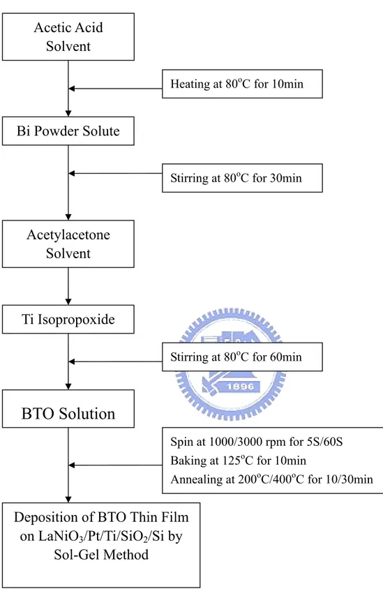
2.1 Experimental Process Flow
We focus on the resistive switching phenomenon of perovskite structure material BTi3O12 (BTO). The experimental flow is shown in Figure 2.1. At first, the resistive
properties are wished to be investigated in prepared samples. If not, the experimental parameters are going to be modified and investigate the switching characteristics again, until the suitable experiment parameters are obtained. After that, material analyses, electrical measurements and mechanisms discussion are all performed and demonstrated in the resistive films. The material analyses, such as SEM, TEM, XRD and SIMS, are used to investigate thickness, crystallization, grain size, inner components distribution, stoichiometry etc. Electrical measurements are the most important parts of the RRAM devices in the experiments. In this part, the distribution of operation voltages, resistance ratio, retention time, endurance test, and stress test are main characteristics which are important criteria of nonvolatile memories (NVMs), investigating the reliable and excellent electrical characteristics of BTO-based RRAM. Finally, because resistive switching mechanisms are unrevealed now, the various experimental conditions, such as various thicknesses, various rapid thermal annealing temperatures effects, and embedded metal speciesetc, are investigated to discuss the carrier conduction and resistive switching mechanisms. The experiment results are discussed and compared with those of other related research results. The instruments used here are also introduced in this section.
2.2 Sample Preparation
The Bi4Ti3O12 (BTO)thin films with embedded metal are mainly investigated for
resistive switching behaviors, and the memory devices are fabricated into a simple structure as shown in Figure 2.2 and Figure 2.3. One is conventional device, metal-insulator-metal structure with a buffer layer between insulator and bottom electrode. The top- and bottom-electrodes are both metallic materials, Pt used here and between them is the Bi4Ti3O12 (BTO) insulator layer and LaNiO3 (LNO) buffer.
The other is the modified device by embedding a thin metal layer within BTO film, and the structure is Pt-BTO-metal-BTO-LNO-Pt. The metal layer was deposited by thermal and electron-beam evaporation. The embedded metal is utilized to diffuse into the BTO film causing the diffusion in the BTO. Taking advantage of this structure, the electrical measurements are performed by probes directly contacting with top- and bottom-electrodes.
There are several sample preparation steps, as showed in Figure 2.4. At first, the 4 inch boron-doped (100) silicon is used as device substrates, and the sample preparation procedure is depicted clearly in the following content.
2.2.1 RCA Cleaning of Silicon Substrate
4 inch boron-doped (100) silicon substrates were cleaned by standard RCA clean, which is the industry standard process to clean and remove contaminants from wafers.
2.2.2. Furnace Oxidation of Silicon Substrate
After RCA clean, the clean Si wafers were posited in the thermal furnace as soon as possible. In the furnace, those wafers were oxidized at 950OC in O2/H2 atmosphere
insulated layer in order to avoid current leakage from the substrate.
2.2.3. Deposition of Bottom Electrode
Ti metal layer, due to the great adhesion for SiO2, was deposited on the SiO2/Si
substrates as an adhesion layer, and followed by Pt bottom-electrode deposited. Both Ti and Pt were deposited by a dual electron-beam evaporation system (EBX-10C) manufactured by ULVAC.
2.2.4. Deposition of LaNiO
3Thin Films
The LaNiO3 thin films were deposited by the rf magnetron sputtering system.
Therefore, the various recipes of the deposition process were controlled by several parameters based on the plasma theorem and the models of the thin films growth. There were many parameters including the chamber pressure, the rf power, the working temperature, the ambient conditions, and the deposition time. The temperature and the ambient conditions could have influences on the defect density, the crystallization, the conductivity, the stoichiometry, and the dielectric constant of thin films. For the accuracy of the atmosphere, the base pressure about 3x10⁻⁶ before sputtering was necessary. To achieve the expected ambient conditions, the flow rate of Ar and O2 was under the control of the MFC, and the working pressure was
controlled by the valves to reach the low pressure where the plasma was generated.
2.2.5. Rapid Thermal Annealing Process of LaNiO
3Thin Films
An as-deposited LNO thin film is performed with a post thermal treatment with rapid thermal annealing. The purpose of the post thermal treatment is to make LNO thin films crystallized with the orientation. In previous reports, the orientation of LNO has the great influences on the resistive switching properties, and better resistive
switching characteristics were obtained on the LNO with (100) orientation. In addition, LNO thin films, in this experiment, are performed with RTA at 600OC in O2
atmosphere for 60s, which have the (100) prefer-orientation. The RTA model is FE-004A made by JETFIRST. [42]
2.2.6. Deposition of Bi
4Ti
3O
12Thin Films
Stoichiometric amounts of the starting materials including bismuth acetate [Bi(OOCCH3)3] and titanium isopropoxide Ti[OCH(CH3)2]4, were dissolved in acetic
acid (CH3COOH) and acetylacetone (C5H8O2). The fabrication flow of the Bi4Ti3O12
(BTO) thin film by sol-gel method is illustrated in Fig. 2.5. Acetic acid was adopted as solvent and heating at 80 oC for 10 min to evaporate the water. Then, the bismuth acetate was added into the acetic acid. The mixture was stirred at 80 oC for 30 min to dissolve the solute into the solvent. After that, the acetylacetone was added into the above solution and then titanium isopropoxide was also added. Then, the mixture was stirred at 80 oC for 1 h to react completely to form the final solution. The Bi4Ti3O12
films were prepared by an acetate precursor sol-gel route on the LNO thin films as the resistive layer. The prepared 0.04 M precursor solution was spin-coated on the LNO/Pt/Ti/SiO2/Si substrates to form the sol-gel film. The parameter of spin-coated is
1000rpm/3000rpm for 5s/60s. Then such deposited layer was heat-treated at 125 oC for 10 min to bake residual water and then annealed at 200 oC /400 oC for 10min/30 min. The coating and heating steps were repeated to obtain the desired film thickness.
2.2.7. Post Deposition Annealing Process of Bi
4Ti
3O
12Thin Films
A post thermal treatment by using post deposition annealing is performed in as-deposited BTO thin films. The purpose of the post thermal treatment is to perform the crystallization of BTO thin films. In addition, the PDA atmosphere (oxygen or
nitrogen) and temperature (from 500℃ to 700℃) can be used to modify the characteristics of the memory devices. The PDA model is FE-004A made by JETFIRST.
2.2.8. Deposition of Top Electrode
The metal masks are utilized, while depositing top-electrodes to achieve various cell sizes easily. The diameters of the dot patterns on the metal mask are 350um, 250um, and 150um, and the electrode areas formed by those metal masks are around 9.62×10⁻⁴, 4.91×10⁻⁴, and 1.77×10⁻⁴cm2, respectively. The Pt top electrode is deposited by e-beam evaporation for top electrode.
2.3 Electrical Measurement and Material Analyses
After fabricating the complete devices, the electrical measurements and the material analyses are performed. Those electrical measurements can provide detailed information and the voltage is applied on Pt top electrode with the Pt bottom electrode grounded.
2.3.1 Current-Voltage (I-V) Measurement
The electrical measurement system consists of a probe station, an Agilent 4155C semiconductor parameter analyzer, an Agilent 8110A pulse generator, an Agilent E5250A low leakage switch, which are controlled by personal computer with the Agilent VEE software and GPIB controller.
The electrical measurement can be sorted into five items: bistable resistive switching measurement, retention test, stress test, endurance test, and other electrical phenomenon measurement. The initial four items are tested for criteria of memory
device and the last item is performed to understand the fundamental properties of the resistive switching memory devices. Moreover, the measurement of bistable resistive switching behaviors is characterized by applying a dc voltage sweeping forth and back between two specific values (in double sweeping mode in 4155C). By this method, the change of the conductivity state in the memory device can be demonstrated to confirm the memory effects induced by the mechanisms we expected.
2.3.2 X-Ray Diffraction (XRD)
Generally, thin films are classified according to the crystallization. There are three types of crystallization, such as amorphous, polycrystalline, and singlecrystalline. X-Ray diffraction analyses are used to investigate the crystal structure and the orientation of our sample. Furthermore, the relations between the crystallization and the heat treatment can be characterized from XRD results. In the experiment, the thin films show either amorphous or poly. Follow Scherrer’s formula, we could calculate the average grain size from XRD illustration:
θ λ cos 9 . 0 × × = B D
The background information of our XRD analyses is that λ=1.5405Å ( ), B is the full width at half maximum (FWHM) of the XRD peak and θ is the diffraction angle. In these analyses, X-ray is made with 0.02 degree beam divergence and operation configuration at 30KV, 20mA.
α
K
2.3.3 Atomic Force Microscopy (AFM)
The atomic force microscopy (AFM) is a very good tool to demonstrate the surface roughness and surface morphology. We use an AFM made by Digital Instruments whose model is Nano-scope III. The root mean square (RMS) value of
roughness of the film is automatically calculated by the AFM software.
2.3.4 Scanning Electron Microscopy (SEM)
Comprehensively, the surface morphology is also an important characteristics compared with those of bulk for the thin films. We could observe the surface micro-morphology and cross section image by SEM. The SEM model is S4700I with highest resolution of 15 Å made by Hitachi.
2.3.5 Transmission Electron Microscopy (TEM)
Electrons form an electron gun are accelerated to high voltages and focused on the samples by the condenser lenses. The samples are placed on a small copper grid a few millimeters in diameter. The static beam has a diameter of a few microns. The samples must be thin enough to be transparent. The transmitted and forward scattered electrons form a diffraction pattern in the back focus plane and a magnified image in the image plane. In order to study the inter-diffusion mechanics and determine the interface thickness, The Philips JEOL JEM9100 Transmission Electron Microscopy (TEM) was used to observe the interface. Furthermore, the TEM can be used to characterize the crystallized states of the films. The maximum magnification is 900000.
2.3.6 Secondary Ion Mass Spectrometer (SIMS)
It is an instrument for microscopic chemical analyses by using a beam of primary ions with energy in the range 5-20 kiloelectronvolts bombards a small spot on the surface of a sample, where the positive and negative secondary ions sputtered from the surface are analyzed in a mass spectrometer.
Resistance switching or not Yes No Conditional Modulation Analysis Electrical Characteristic Measurement Bistable Switching Reliability Test Stress Retentio XRD SEM TEM
Possible Conduction Mechanism
Results and Discussion Endurance
Material Mirco-morphology and Componential Analysis
Modification to Process
AFM Sample preparation
SIMS
Figure 2.2 The cross section view of conventional BTO structure Top electrode-PT (80nm) Pt/Ti BTO-2
Si substrate (100)
SiO
2(200nm)
LNO
BTO-1 Embedded Metal Top electrode-Pt (80nm)LNO
BTOSiO
2Si substrate (100)
Pt/TiR.C.A Clean & Oxidation
Synthesis of LaNiO3 Powder
and Preparation for Target
Deposition of LNO Bottom Electrode
RTA and Dgas for LNO Bottom Electrode
Deposition of BTO Thin Film by Sol-Gel Method
RTA for BTO Thin Films
Deposition of Pt Top Electrode
Embedded
RTA for Diffusion-doped BTO Thin Films
Deposition of the embedded metal layer by E-beam
Evaporation Preparation for BTO
Solution
Deposition of Pt/Ti buffer layer Si Substrate (100)
Acetylacetone
Solvent
Bi Powder Solute
Ti Isopropoxide
Stirring at 80oC for 60min Stirring at 80oC for 30min Heating at 80oC for 10min
Annealing at 200oC/400oC for 10/30min Baking at 125oC for 10min
Spin at 1000/3000 rpm for 5S/60S
Deposition of BTO Thin Film
on LaNiO
3/Pt/Ti/SiO
2/Si by
Sol-Gel Method
BTO Solution
Acetic Acid
Solvent
Chapter 3
Experimental Results and Discussion
3.1 Pure BTO thin film
The criteria for a perfect nonvolatile memory device includes low operation voltage, low power consumption, long retention time, small cell size, high operation speed, low cost, high endurance, non-destructive readout, and simple structure. There are few reports about the memory effects and resistive switching behaviors in the BTO thin films for RRAM applications nowadays. However, recently, reproducible resistive switching in bismuth titanate (BTO) deposited by electron cyclotron resonance sputtering was successively reported. [XX] In the previous experiment, the pure BTO thin film was deposited by Sol-Gel method and performed the bistable resistive switching characteristics. However, there are still some drawbacks of the BTO-derived memory devices. In this thesis, it is interesting to promote the properties of this kind of device, like endurance and operation voltage, which are important issues for currently CMOS process.
3.1.1 Thickness of pure BTO thin film
The thickness of the original pure BTO thin film is about 45nm ~ 60 nm. Based on the previous experimental data, the forming voltage was located at the range of -4V~ -6V. This would be a big problem for application. As we know, BTO thin film was deposited by Sol-Gel method and repeated coating for 3 times to attain the thickness wanted. Nevertheless, there is a factor needed to be taken into consideration – Roughness. While coating such thin film in repeat, it doubtlessly increases the surface roughness in the aspect of micro-investigation. For this reason, we test BTO thin film in thinner thicknesses to keep a flat surface and try to diminish
the effect of roughness. In this section, we are talking about effect of thinner switching oxide on electrical properties. The BTO thin film is finished by coating for 2 times and its equivalent thickness is about 20 nm.
3.1.2 Forming process
Before any resistive switching is performed, the device is initially at an original-state (O-state) with higher resistance than OFF-state. In Figure 3.1, the voltage sweeps close to -4V and then a sudden increase in the conduction current is observed and limited at the current compliance of 20 mA, switching the device to ON-state. The forming process means a high DC bias is applied on the memory device to switch it from original-state to ON-state. During the forming process, the leakage current shows a hysteretic phenomenon in I-V curve with the double sweeping mode in Agilent 4155C.
3.1.3 Operation mode and voltage
After forming process, the memory device remains at ON-state. Then, we need a positive voltage to switch the memory device back to the OFF-state and this is what we call turn-off process. If the memory is switched back to the ON-state, this is a turn-on process. In previous research, even though BTO thin film belongs to non-polar switching, the best mode is located at negative turn-on and positive turn-off mode. From now on, in this thesis, we only sweep for this best mode to investigate the electrical properties. The range of the operation voltage is located at -1.2V ~ -3.8V, but depicts a larger variation.
3.1.4 Memory test for endurance
In nonvolatile memory, there is an important indication for using – Endurance. Figure 3.2 depicts the endurance test for pure BTO thin film. This is an unacceptable result. The switching cycles are less than 10. Therefore, post deposition annealing is brought in to solve such issue.
3.1.5 Thermal effect of post deposition annealing
As we know, annealing is helpful for repairing the crystalline and then improves the electrical performance. Unfortunately, it seems that post annealing does not give any promotion in this memory device, but leads to failure in the end. It is deduced that post annealing make grain become larger with high temperature and then increases the leakage current dramatically. However, thickness of BTO thin film is about 20~30nm. After post annealing at higher temperature, voltage drives thin film break down easily.
3.1.6 Summary for thinner pure BTO thin film
From these investigations of electrical properties, there are some disadvantages of BTO thin film. First, the unstable turn-on voltage increases the difficulty for RRAM applications. Miss read error between turn-on and turn-off voltage would be a serious problem in real operation. Second, reliability test for endurance is very poor, which is not suitable for applications. Third, we tried to improve its electrical properties with post annealing, but failed. That is to say that thinner BTO film could not tolerate such high temperature. Therefore, in the next section, we have a little change on structure by embedding a metal layer in between. Some interesting phenomenon are investigated and discussed later.
3.2 The effect of embedded metal in BTO thin film
Recently, many reports about the embedded perovskite thin films for non-volatile memory are proposed for RRAM application were investigated, and many kinds of embedded metal materials have been investigated and Liu et al., and Nb-doped SrTiO3 films by Xiang et al. Based on the research of perovskite material SrZrO3 with
embedded metal, electrical properties such as operation voltage and endurance are greatly improved. BTO thin film, as known a type of perovskite structure, it is quite interesting for us to test embedded metal on it. Description about details will be referred in the following sections.
3.2.1 Materials for embedded metal
There have been many materials tested for embedded metal in perovskite
structure, such as Pt, Pd, Mo, Cr, and Cu. However, it seems that device with Cr embedded has the better properties than else. It is known that Cr is a low work function metal in comparison to high work function metal Pt. In the thesis, we focus on these two different metals and give a comparison between them.
3.2.2 The effect of thermal treatment
There is an important process in this thesis, named post deposition annealing, which is abbreviated as PDA. The device will experience a high temperature process (500oC, 600oC, 700oC) in N2 ambient for 30 seconds before depositing top electrode.
The object is to dismiss the thermal stress remained in metal materials and further to enhance the quality of thin films. It is worthy to be mentioned that the embedded metal diffuses in BTO thin film with the help of thermal treatment, and then the resistive switching property is investigated and discussed.
![Figure 1.1 A schematic of an MTJ memory cell. Arrows indicate possible directions of magnetic movement [9]](https://thumb-ap.123doks.com/thumbv2/9libinfo/8254589.171831/32.892.174.722.118.608/figure-schematic-arrows-indicate-possible-directions-magnetic-movement.webp)
![Figure 1.6 Equivalent circuit of an array for the write operation of a given bit resistor [21]](https://thumb-ap.123doks.com/thumbv2/9libinfo/8254589.171831/34.892.163.729.518.986/figure-equivalent-circuit-array-write-operation-given-resistor.webp)