國立交通大學
電子工程學系 電子研究所碩士班
碩 士 論 文
寬頻矽基板覆晶片結構及低功率基底趨
動混頻器之設計
Design of Broadband Si Carrier Flip-Chip
Structure and Low-Power Bulk-Driven Mixer
研 究 生 : 李俊興
指導教授 : 郭建男 教授
寬頻矽基板覆晶片結構及低功率基底趨
動混頻器之設計
Design of Broadband Si Carrier Flip-Chip
Structure and Low-Power Bulk-Driven Mixer
研 究 生 : 李俊興 Student : Chun-Hsing Li
指導教授 : 郭建男 Advisor : Chien-Nan Kuo
國 立 交 通 大 學
電子工程學系 電子研究所碩士班
碩 士 論 文
A Thesis
Submitted to Department of Electronics Engineering & Institute of Electronics College of Electrical Engineering
National Chiao Tung University For the Degree of
Master In
Electronic Engineering July 2007
Hsinchu, Taiwan, Republic of China
寬頻矽基板覆晶片結構及低功率基底趨動混頻器之設計
學生 : 李 俊 興 指導教授 : 郭 建 男 教授
國立交通大學
電子工程學系 電子研究所碩士班
摘要
本篇論文提出一個適用於毫微米波頻段之無凸塊覆晶片結構,以及高效能、 低功率射頻積體電路之設計。 本論文所提之覆晶片技術,利用金金熱壓合技巧,使得覆晶片結構能夠提供 從晶片上之微帶線到戴具上之共平面帶線之間連續的特徵阻抗及平順的電流流 動。參數最佳化顯示,此覆晶片結構之結構參數對於頻率響應並不敏感。量測結 果顯示,頻率到 50GHz 之前,具有 1.7dB 的插入損耗,及 15dB 的返迴損耗。此 覆晶片結構具有寬頻的特性,並且不需要額外的匹配網路。 電壓控制振盪器之設計,乃利用該覆晶片技術,整合微機電之高品質因素電 感,及 CMOS 晶片,分別設計二個操作於 5GHz 之電壓控制振盪器,以達成低功率, 高效能的目的。其中一個電壓控制振盪器,設計為具有高的優劣評比,在功率消 耗僅 1.03mW 情況下,其優劣評比為 191.2dB,頻率調整範圍為 7.9%;另一個電 壓控制振盪器,設計為具有寬的頻率調整範圍,在功率消耗僅為 1.08mW 情況下,其頻率調整範圍為 20.2%,優劣評比為 188dB。操作電壓皆為 1V。 混頻器之設計,應用於無線近身網路,乃利用 LO 基底趨動之電路架構,結 合切換級及轉導級於單一顆電晶體,以達成低電壓,電功率之目的。並且利用變 形之 Volterra 級數進行基底趨動混頻器之最佳化設計,發現電壓轉換增益和三 階互調乘積的本質來源分別源自於二階和四階非線性電流。量測結果顯示,當基 底趨動混頻器操作於 1.4 GHz 及 1V 之操作電壓下,具有 16dB 的電壓轉換增益, -0.5dBm 的第三階交會點,18.1dB 的返迴損耗,及 19.65dB 的雜訊指數,其等待 功率消耗為 0.25mW,操作功率消耗為 0.69mW。
Design of Broadband Si Carrier Flip-Chip Structure and
Low-Power Bulk-Driven Mixer
Student: Chun-Hsing Li Advisor: Prof. Chien-Nan Kuo
Department of Electronics Engineering & Institute of Electronics
National Chiao-Tung University
ABSTRACT
This thesis proposes designs of a bump-less flip-chip structure applicable to millimeter-wave frequency, and radio frequency (RF) integrated circuit with low power and high performance.
The proposed flip-chip structure using Au-Au thermo-compression technique to make the flip-chip structure provides continuity of characteristic impedance from the on-carrier CPW line to the on-chip microstrip line, as well as smooth current flow. Parameter optimization further indicates that the structural parameters in transition are insensitive to the frequency response. Measurement results show that return loss is better than 15dB and insertion loss smaller than 1.7dB up to 50GHz. The transition structure has broadband performance without any external matching network.
Flip-chip technique is employed to integrate with high-quality (Q) MEMS inductor and CMOS chip to design two VCOs operating in 5 GHz for the purpose of high performance and low power consumption. One of the two VCOs is designed with high figure-of-merit (FOM). Under power consumption of 1.03mW, the VCO has FOM of 191.2dB and tuning range of 7.9 %. The other is designed in wide tuning range. The VCO has tuning range of 20.2% and FOM of 188dB consuming only
1.08mW. The supply voltage is 1V in these two VCOs.
As for mixer design at the application of wireless body area network (WBAN), a bulk-driven architecture is adopted to merge switching stage and transconductance stage into a single transistor for the objectives of low voltage and low power operation. Variant Volterra series is also used for the optimization of bulk-driven mixer. The insight of nonlinear operation of bulk-driven mixer is gained that the intrinsic conversion gain and the third-order inter-modulation product (IM3) originate from the second-order and fourth-order nonlinear currents, respectively. The bulk-driven mixer operates in 1.4 GHz under supply voltage of 1V. The measurement results show that the voltage conversion gain is 16dB, the input return loss is 18.1dB, the IIP3 is -0.5dBm, and the NF (DSB) is 19.65dB. The power consumption is 0.25mW in standby mode and 0.69mW in operating mode.
誌謝
得以順利完成此篇論文,首要感謝的是我的指導教授郭建男教授這兩年來的悉 心指導,使我在射頻積體電路設計及微波領域中有所了解,並且學習到嚴謹的研 究態度與方法。此外,感謝鄭裕庭老師在系統封裝計劃中給予我很多的指導。在 此向老師們獻上最深的敬意。 感謝昶綜、鈞琳、明清、鴻源、子元、子倫、益民學長們的不吝指導,在許多 方面給予我非常大的幫助;感謝一起研究、一同奮鬥、互相鼓勵的宗男、燕霖, 以及易耕、煥昇、昱融、培翔、信宇、名伽、家瑋學弟們。由於有了你們,實驗 室就像一個溫馨的大家庭,非常感謝大家這兩年來的照顧。另外還要感謝國家晶 片中心在晶片製作上所提供的協助。 最後,要特別感謝我的家人給我的栽培與支持,以及燕霖的陪伴與打氣,使我 能順利快樂地度過碩士這段生涯。還有很多其他要感謝的人,在此一併謝過。 李俊興 九十六年 七月CONTENTS
ABSTRACT (CHINESE)
………...…...iABSTRACT (ENGLISH)
………...iiiACKNOWLEDGEMENT
………...vCONTENTS
...…...viTABLE CAPTIONS
... viiiFIGURE CAPTIONS
...ixChapter 1 Introduction
...11.1 Motivation
...11.2 Thesis
Organization
...4Chapter 2 Broadband Flip-Chip Interconnect for Millimeter-Wave
Silicon Carrier System-on-Package
...62.1 Introduction
...62.2 CPW to Microstrip Line Transition Structure Design
...92.2.1 Transmission Line Design ...10
2.2.2 Transition Structure Design ...13
2.2.3 Detuning Effect...16
2.2.4 Calibration Method ...17
2.3 Measurement Results and Discussion
...242.3.1 Measurement Results of the Microstrip Line...24
2.3.2 Measurement Results of the CPW ...25
2.3.3 Measurement Results Using TRL Calibration ...26
2.3.4 Trouble Shooting...29
2.3.5 Measurement Result Using Multi-Line De-embedding Method .31
Chapter 3 A Low Power 5GHz Voltage-Controlled Oscillator
Utilizing SoP Technique
...333.1 Introduction
...333.2 VCO
Circuit
Design
...343.2.1 MEMS Inductor Design Flow...37
3.2.2 The Design of VCO with a High FOM...39
3.2.3 The VCO with a Wide Tuning Range ...48
3.3 The Layout of the Chip and the Carrier
...52Chapter 4 Design of the Low Power and Low Voltage Bulk-Driven
Mixer
...554.1 Introduction
...554.3 Low Power Bulk-Driven Mixer Design
...724.3.1 Large Signal Analysis ...73
4.3.2 AC Response...75
4.3.3 Individual Response...82
4.3.4 Current Mirror Bias Circuit ...84
4.3.5 Matching Circuit ...85
4.4 Measurement
Results
...864.4.1 On-Wafer Measurement Setup...86
4.4.2 Measurement Results...87
4.5 Re-Tapeout of the Bulk-Driven Mixer
...93Chapter 5 Summary and Future Work
...975.1 Summary
...975.2 Future
Work
...98References
...99Appendix A Fundamental of Phase Noise
...102Vita
...109TABLE CAPTIONS
Table 3.1. The summary of MOS varactor of group 1 and group 2………...40
Table 3.2. Summary of post-simulation result of high performance VCO………...47
Table 3.3. The summary of the characteristic of the varactors………..48
Table 3.4. Performance summary of the wide tuning range VCO………51
Table 3.5. Summary of SoP versus SoC………52
Table 4.1. Second-order nonlinear current at w1± w2 and 2w2……….67
Table 4.2. Third-order nonlinear current for response at 2w1± w2………...68
Table 4.3. Third-order nonlinear current for response at 3w2………...68
Table 4.4. Fourth-order nonlinear current for response at |2w1+w2+ w3|…………..70
Table 4.5. Fourth-order nonlinear current for response at 3w2± w2|……….71
Table 4.6 Comparison of the proposed bulk-driven mixer with the prior arts……..93
Table 4.7 Summary of the circuit performance of the re-tapeout bulk-driven mixer………...96
FIGURE CAPTIONS
Fig. 1.1. SoP solution...2 Fig. 2.1. The transition structures: (a) staggered bumps. (b) locally matching
technique. (c) high impedance compensation…………...7 Fig. 2.2. The test structure for characterization of the proposed bump-less flip-chip
transition from CPW line on the Si carrier to microstrip line on the chip fabricated in a standard 0.18 um CMOS process……….9 Fig. 2.3. The microstrip line structure in standard 0.18um CMOS technology, (a)
cross-section view. (b) top view…...10 Fig. 2.4. Frequency response of characteristic impedance of the microstrip line…11 Fig. 2.5. The CPW structure in carrier. (a) cross-section view (b) top view……….12 Fig. 2.6. Frequency response of characteristic impedance of the CPW…………...13 Fig. 2.7. Top view of the transition structure from CPW to the microstrip line. The
electrical performance is evaluated by sweeping the parameters, Gap and Length, by an EM simulator………..……….14 Fig. 2.8. HFSS simulation results of the test structure. The reference plane is
de-embedded to the location as shown in Fig. 2.19, the same as that in TRL measurements……….15 Fig. 2.9 The microstrip line in flipped condition. The silicon carrier detunes the
characteristic of the microstrip line………16 Fig. 2.10 Analysis of detuning effect of the microstrip line under consideration
indicates that the line impedance is deviated around 2-Ω………..17 Fig. 2.11 Block diagram of a general measurement setup………18 Fig. 2.12 Block diagram and signal flow graph for the THRU connection………..18
Fig. 2.13 Block diagram and signal flow graph for the REFLECT connection……19 Fig. 2.14 Block diagram and signal flow graph for the LINE connection…………20 Fig. 2.15 Multi-line for de-embedding………..22 Fig. 2.16. Micrograph of the microstrip line fabricated by standard CMOS 0.18um
technology………..24 Fig. 2.17. Measurement results of the microstrip line: (a) return loss. (b) insertion
loss………..25 Fig. 2.18 Measurement results of the CPW: (a) characteristic impedance. (b) alpha
(c) beta………26 Fig. 2.19 Pictures of flip-chip structure. (a) on-wafer probing. (b) SEM photo of flip-chip structure. (c) Bonding interface in transition structure shows 2um
misalignment………..27 Fig. 2.20. Reference planes of the flip-chip test structure by TRL measurements and
EM simulations………27 Fig. 2.21. Comparison between simulation and measurement data, (a) return loss
and (b) insertion loss. Simulation is based on initial assumption of silicon conductivity of 10S/m………..28 Fig. 2.22 Variation of characteristic impedance of CPW with different gap width..29 Fig. 2.23 Comparison between simulation and measurement data, (a) return loss and
(b) insertion loss. Simulation data with revised the CPW line dimensions and the substrate conductivity (Sx1_Sim_75 S/m Si) agree well with measurement data………...30 Fig. 2.24 Measurement results using multi-line de-embedding method. (a) return
loss. (b) insertion loss……….31 Fig. 3.1. Block diagram demonstrates the integration by SoP technique…………..33 Fig. 3.2 VCO using the flip-chip technique………..34
Fig. 3.3 VCO topology using a conventional LC cross-coupled pair. All CMOS transistors are to make VCO have lower flicker noise and thermal noise contributed to the phase noise………35 Fig. 3.4 VCO topology using a conventional LC cross-coupled pair………...35 Fig. 3.5 Co-simulation of Spectre RF and the MENS inductor from HFSS and
Designer………...37 Fig. 3.6 The layout of the MENS inductors. (a) inductance of 5nH at 5GHz with
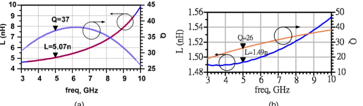
differential Q of 43 used in the VCO with a high FOM. (b) inductance of 1.5nH at 5GHz with differential Q of 37 used in the VCO with a wide tuning range………...38 Fig. 3.7 The inductance value and the Q of the MENS inductors (a) used in the
VCO with a high FOM. (b) used in the VCO with a wide tuning
range………...39 Fig. 3.8 The impedance and the Q of the LC tank under different tuning voltages. (a)
the impedance (b) the Q………...41 Fig. 3.9. The FOM of the VCO with a high FOM versus the finger number of the
switching transistors at different corner cases. (a) TT. (b) SS. (c) FF……42 Fig. 3.10. The dependence of the output phase noise on Cf under different corner
cases………...43 Fig. 3.11. (a) The oscillation frequency. (b) The output power of the high FOM
VCO before and after the output buffer………...44 Fig. 3.12. (a) the phase noise at 1MHz offset. (b) The FOM versus the tuning
voltage………..44 Fig. 3.13. The oscillation frequency and the output power versus the tuning voltage. (a) The oscillation frequency. (b) The output power………46 Fig. 3.14. The phase noise and the FOM versus the tuning voltage, (a) the phase
noise at 1MHz offset. (b) the FOM………..46
Fig. 3.15. Phase noise. SoP versus SoC………47
Fig. 3.16. The impedance and the Q of the LC tank under different tuning voltages. (a) the impedance (b) the Q. ………..49
Fig. 3.17. (a) the oscillation frequency (b) the output power, versus the tuning voltage. ………49
Fig. 3.18. The phase noise and the FOM versus the tuning voltage, (a) phase noise at 1MHz offset. (b) the FOM. ……….50
Fig. 3.19. (a) The oscillation frequency. (b) The output power……….50
Fig. 3.20. The phase noise and the FOM versus the tuning voltage. (a) the phase noise at 1MHz offset. (b) the FOM. ………51
Fig. 3.21. Phase noise. SoP versus SoC………51
Fig. 3.22. The chip and the carrier layout. The layout outside the red square is the carrier layout. ………...53
Fig. 3.23. Measurement setup for the on-wafer measurement………..54
Fig. 4.1. Single-balanced Gilbert Mixer. ………56
Fig. 4.2. Applications of WBAN on the medical service………57
Fig. 4.3. Single-balanced bulk-driven mixer. ……….58
Fig. 4.4. The half circuit of the bulk-driven mixer for the nonlinearity analysis…60 Fig. 4.5. The equivalent circuit for the nonlinear analysis………..61
Fig. 4.6. The equivalent circuit for the first-order response………63
Fig. 4.7. The equivalent circuit for the second-order nonlinear response………...65
Fig. 4.8. The proposed low power and low voltage bulk-driven mixer…………..72
Fig. 4.9. The half circuit of the bulk-driven mixer for the nonlinearity analysis…76 Fig. 4.10. The comparison of the simulation and the calculation results of the first-order response at the frequencies of wRF1 and wLO.……….76
Fig. 4.11 The comparison of the simulation and the calculation results of the second-order nonlinear response at the frequencies of wRF1-wRF2 and wRF1+wRF2………...77 Fig. 4.12 The comparison of the simulation and the calculation results of the
second-order nonlinear response at the frequencies of wRF1-wLO and 2wRF1. ………...77 Fig. 4.13. The comparison of the simulation and the calculation results of the
third-order nonlinear response………..78 Fig. 4.14 The comparison of the simulation and the calculation results of the
fourth-order nonlinear response at the frequency of the IM3…………..78 Fig. 4.15. Comparison of the simulation and the calculation results of the first-order response………79 Fig. 4.16. Comparison of the simulation and the calculation results of the s
econd-order response………79 Fig. 4.17. Comparison of the simulation and the calculation results of the
second-order response………..80 Fig. 4.18. Comparison of the simulation and the calculation results of the third-order response………80 Fig. 4.19. Comparison of the simulation and the calculation results of the
fourth-order response………...80 Fig. 4.20. Nonlinear mixing to the DC at the drain node. This DC offset at the VDS
will increase the consumed drain current………81 Fig. 4.21. Comparison of calculation and simulation results in operation current…82 Fig. 4.22 The individual contribution to the voltage conversion gain………83 Fig. 4.23. The individual contribution to the IM3……….83 Fig. 4.24. IIP3 versus VGS under different corner cases. (a) use voltage to bias. (b)
use current mirror to bias………..84
Fig. 4.25. The diagram of the current mirror bias circuit………..85
Fig. 4.26. Measurement setup for the on wafer measurement………..86
Fig. 4.27. PCB Layout………...86
Fig. 4.28. Micrograph of the bulk-driven mixer………87
Fig. 4.29. The S11 measurement results. (a) LO is off. (b) LO is applied…………88
Fig. 4.30. The measurements of the conversion gain, the IM3 gain, and the IIP3 versus VGS. (a) voltage conversion gain. (b) the IM3 gain. (c) the IIP3..88
Fig. 4.31. The measurements of the conversion gain, and the IIP3 versus VGS. (a) voltage conversion gain. (b)IIP3………..89
Fig. 4.32. The measurements of the conversion gain, and the IIP3 versus the LO power. (a) voltage conversion gain. (b)IIP3………...90
Fig. 4.33. The measurements of the conversion gain versus the IF frequency…...90
Fig. 4.34. The measurements of the conversion gain versus the IF frequency…...91
Fig. 4.35. The measurements of the DSB NF versus the IF frequency……….92
Fig. 4.36. The measurements of the IF and the IM3 versus the RF power……….92
Fig. 4.37 The output buffer……….94
Fig. 4.38. The simulation results……….94
Fig. 4.39. The simulation results……….95
Fig. 4.40. The simulation results……….95
Fig. 4.41. The simulation results……….95
Fig. 5.1. Mixer topology for twice downconversion……….98
Fig. A.1. Influence of strong interference on dynamic range of receiver, (a) a strong interference adjacent to desired signal (b) practical spectrum in VCO output (c) impact of interference on the desired signal………102 Fig. A.2. The spectrum of the phase noise. The 1/f3 region is mainly contributed
by the flicker noise and the 1/f2 region is dominated by thermal
noise………...103 Fig. A.3. An equivalent systems for excess amplitude and phase response in phase
noise analysis………104 Fig. A.4. Evolution of circuit noise into phase noise………..106
Chapter 1
Introduction
1.1 Motivation
The growing demand of wireless communications has driven many emergent commercial applications. The trend of RF front-end circuit design for these applications is leading to Silicon (Si) CMOS technology for low cost. Much attention is paid to the applications demanding low power consumption, such as wireless body area networks (WBAN) [1], to extend lifetime of battery. Besides, supply voltage shall be low in these applications.
Although CMOS technology has an advantage of low cost, its silicon substrate is very lossy so that it is hard to build on-chip passive components with high-quality. To tackle the issue of Si lossy substrate, the System-on-Package (SoP) technique has been very attractive [2]. Fig. 1.1 demonstrates the SoP technique. Instead of building everything on a single chip, modules of RF transceiver components are designed and fabricated in separate dies, and then fully integrated onto a single carrier as a multi-chip module. SoP also integrates high-quality passive components, such as high Q MEMS inductor, filter, and antenna, onto the carrier. Using Si substrate can low
down the cost and increase the circuit integration.
The most essential part of SoP is the flip-chip interconnection between the CMOS chip and the carrier. This transition structure shall have good return loss and low insertion loss covering a wide-frequency range so that it does not influence CMOS chip performance. This thesis proposes the design of a bump-less broadband flip-chip transition structure for high frequency applications. Its electrical performance is tested by connecting transmission lines on a Si carrier and on a chip circuit fabricated in a standard 0.18µm CMOS process. Chip-carrier assembly is realized by Au-Au thermal compression bonding. With near zero bump height, the impedance variation is so small that the structure provides very good interconnection of good return loss and
Carrier
CMOS Wafer
Carrier
Interconnect is critical!
low insertion loss.
On-chip inductor is a key passive component in VCO design. However, the lossy substrate degrades the quality factor (Q) of an on-chip inductor. Hence VCO using an on-chip inductor usually consumes large power to compensate the loss from LC tank. To conquer the lossy substrate, we use the SoP technique to integrate CMOS technology with high-Q MEMS inductors to design two VCOs operating in 5GHz. Thanks to the high-Q MEMS inductor, the VCOs feature in high performance under low power consumption.
Gilbert mixer is usually used to down-convert RF signal to intermediate frequency (IF) in low-IF receiver. However, with the fast development of CMOS technology, the supply voltage is reduced to lower level. This reduction of supply voltage makes the Gilbert mixer hard to realize because of stack-up of two transistors. In order to operate in low supply voltage, mixer with cascode topology should be avoided. A good candidate for low voltage operation is the bulk-driven mixer which takes the advantage of MOSFET with inherent four terminals [3]. The bulk-driven mixer can then be used at the application of WBAN, which demands low supply voltage and low power consumption.
The thesis proposes a low power and low voltage bulk-driven mixer demonstrating high conversion gain and good linearity for the application of wireless body area
network (WBAN). Volterra series is used to analyze the nonlinearity of bulk-driven mixer. The insight of nonlinear operation of bulk-driven mixer is gained that the mixer belongs to the type of weakly nonlinear mixer. This insight is different from the prior arts claiming that bulk-driven mixer is a type of switching mixer [4-6]. The individual contribution from each nonlinear source to conversion gain and linearity is obtained to decide the optimal bias condition while the trade-off between conversion gain and linearity is taken into account.
1.2 Thesis Organization
In Chapter 2 we discuss the design of broadband flip-chip interconnect for millimeter-wave Si carrier system-on-package. This discussion includes transmission line design, transition structure design, calibration method, and the measurement results.
In Chapter 3 two VCOs are designed by using the SoP technique to integrate a CMOS chip with a high-Q MEMS inductor. The design procedure of MEMS inductor and VCOs, simulation result, and measurement consideration are discussed.
In Chapter 4 low power and low voltage bulk-driven mixer is designed. This chapter includes the overview of the fundamental of nonlinearity analysis using variant Volterra series, comparison of simulation results and calculation results, individual nonlinear contribution, how to decide the optimal bias condition, input
matching mechanism, bias circuit, and measurement results. Finally Chapter 5 is the conclusion and future work.
Chapter 2
Broadband Flip-Chip Interconnect for
Millimeter-Wave Silicon Carrier
System-on-Package
2.1 Introduction
In the development of advanced microwave and millimeter-wave systems, the interconnect design is an essential part of the system electrical performance. As far as circuit design is concerned, the interconnection shall provide good return loss and low insertion loss over the signal frequency range. Of the available multi-chip packaging techniques, the flip-chip technique appears better than the wire-bonding technique for microwave and millimeter-wave packaging due to less and more reproducible parasitic effects [7]. It has been shown in numerous articles that the electrical performance of the conventional wire bond leads to an increase in return loss and insertion loss as the frequency or interconnection distance is increased. The flip-chip interconnect is often employed for connection because of the advantages of low parasitic element since the short interconnection length, the low assembly cost, and
the high reproducibility, as compared to the conventional wire bond. When the flip-chip technology is used, there are two main issues that determine the characteristics of a flip-chip monolithic microwave integrated circuit (MMIC): detuning of the circuit on chip due to its proximity to the motherboard and the reflection at the bump interconnect.
Most flip-chip technology adopts a soldering bump structure [8, 9]. Signal propagation inevitably encounters discontinuity. Operated at low frequencies, the flip-chip interconnect can be still considered as a simple transition of no significant impact on electrical performance in terms of return loss and insertion loss. This gives great freedom to circuit design and system integration. As to the millimeter-wave
(a) (b)
(c)
Fig. 2.1. The transition structures: (a) staggered bumps. (b) locally matching technique. (c) high impedance compensation.
modeling on parasitic and incorporated into circuit design.
Many transition structures have been proposed for the design at millimeter-wave frequency, like those as shown in Fig. 2.1[9-11]. The basic idea is that of compensation, i.e., reducing parasitic capacitance at the transition by adding an inductive counterpart. Three approaches are investigated here: staggered bumps, a locally matching technique, and an on-carrier solution employing a high-impedance line section. As to the staggered bumps in Fig. 2.1(a), compensation is achieved by staggering center conductor and ground bumps. The center conductor of the chip is elevated and the field concentrated in the air region, which leads to a decrease in capacitance. The clear disadvantage, however, is that the interconnection now consumes additional expensive chip area. Moreover, this approach is not compatible with common chip layouts, but requires a customized chip design. In brief, this approach is effective, but not generally recommendable.
Fig. 2.1(b) shows the locally matching technique. The ground conductor is retreat by ∆ to reduce the parasitic capacitance. The typical value of ∆ for good return loss is around 100um which increase the chip area, and thus raise the cost.
In the case of the high impedance compensation technique as indicated in Fig. 2.1(c), it is clear that the return loss is improved at low frequency band only. The high impedance line which contributes more parasitic inductance will degrade the high
frequency performance, that is, it is usually narrow band in principle.
These three compensation techniques require impedance matching to compensate the parasitic inductance and capacitance due to the soldering bump and the bumping pad, respectively. Nevertheless, matching optimization causes much time consumption and very often limited bandwidth. In this chapter, bump-less flip-chip interconnect by using Au-Au thermo-compression technique for the applications at millimeter-wave frequency band is discussed. This flip-chip interconnect has the advantages of easy design, no external matching network, small area, and broadband performance.
2.2 CPW to Microstrip Line Transition Structure Design
Transition of CPW to microstrip line is widely used in packages, on wafer measurement of microstrip based MMIC, and it also interconnects in hybrid circuits
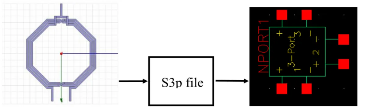
Fig. 2.2. The test structure for characterization of the proposed bump-less flip-chip transition from CPW line on the Si carrier to microstrip line on the chip fabricated in a standard 0.18 um CMOS process.
including both microstrip and CPW. So CPW to microstrip line transition is adopted to test the bump-less flip-chip technology up to millimeter-wave frequency. The test structure as shown in Fig. 2.2 is designed connecting transmission lines, a microstrip line fabricated in a 0.18 µm CMOS chip and two CPW lines built on a silicon carrier. Bump-less contacts apply Ni/Au deposited layers for chip bonding. In this design, EM signal will be transmitted from one CPW line on the silicon carrier to the other via two flip-chip interconnects and the microstrip line. Essentially this might be considered as the worst scenario of possible transitions. As signal loss through the microstrip line is very low, the symmetric structure design provides a full investigation on the electrical performance of the flip-chip interconnects.
2.2.1 Transmission Line Design
The design target of a transmission line is to decide the physical dimension corresponding to 50Ω characteristic impedance for the measurement purpose.
(i) Microstrip Line
M
6M
1SiO2
W
6.52um
2.34um
PASS
4
=
r
ε
SiO2
M
1M
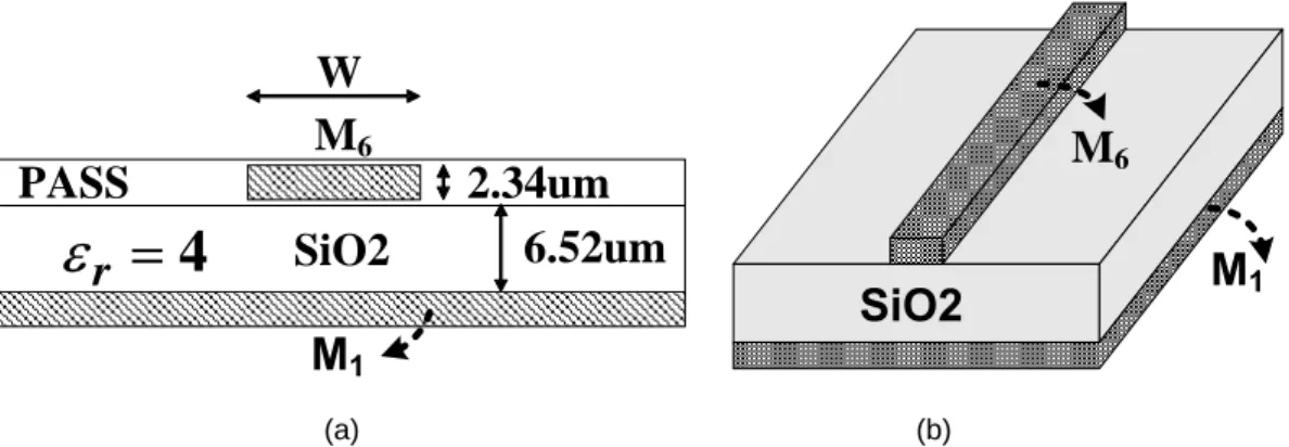
6 (a) (b)Fig. 2.3. The microstrip line structure in standard 0.18um CMOS technology, (a) cross-section view. (b) top view.
Fig. 2.3 shows the cross-section view and top view of a microstrip line fabricated in standard 0.18um 1P6M CMOS technology. The microstrip line consists of the top metal layer (M6) as the signal line and the bottom metal layer (M1) as the ground plane. The only adjustable parameter is the center width of signal line which is set as 10.5um to obtain 50Ω characteristic impedance. The EM simulation result of Zo versus frequency is shown in Fig. 2.4. As indicated from the plot, Zo is dispersive at low frequency range. This phenomenon can be understood from the equation of characteristic impedance, (2-1). It is found that dispersion in low frequency is caused by the existent dielectric loss and the conductor loss. If the dielectric and conductor is perfect, i.e. no loss, the characteristic impedance will remain constant over the signal frequency. Although Zo deviates from 50Ω at low frequency, this does not mean that return loss degrades too. Keep in mind that the S parameter is defined for an infinite
0 20 40 60 80 100 48 50 52 54 56 Zo (Ohm) freq (GHz)
jwC
G
jwL
R
Z
o+
+
=
(2-1)(ii) Coplanar Waveguide (CPW)
The cross-section view and top view of a CPW are shown in Fig. 2.5. The CPW consists of three conductors which center metal is signal line and the other two are ground layer. The CPW metal is made of electroplated Cu of 5um thickness. The design parameters for 50Ω line impedance are the width of center metal and the gap between signal line and ground line. The signal width is set as 10.5 um, the same as the signal width of microstrip line, to have continuous line impedance at the transition. Hence the only changeable parameter is the dimension of the gap. “gap” is set as 7.2um to have 50Ω characteristic impedance. The simulation result of Zo is shown in Fig. 2.6 which indicates that Zo at high frequency is not close to 50Ω. It is since an error in simulation setup, but this does not affect the return loss too much. After removing the error in setup, the gap ought to be 8um to own 50Ω line impedance.
Silicon
SiO2W
2.1um
5um
gap
SiO2 Si3N4Cu
400um
9
.
11
=
r
ε
(a) (b) Fig. 2.5. The CPW structure in carrier. (a) cross-section view (b) top view.The frequency dependence at low frequency is different from the case in the microstrip line. This is since that the conductor loss is greater than the dielectric loss at low frequency in microstrip line; however, in the CPW, the loss from silicon substrate is larger than the conductor loss. Consequently, from (2-1), the Zo of the microstrip line and the CPW will approach infinity and zero, respectively, at zero frequency.
2.2.2 Transition Structure Design
After decision of the physical structure of the microstrip line and the CPW, the transition of CPW to microstrip line needs to be carefully designed to have continuous electromagnetic filed and smooth current flow. The grounds are designed in the shape as shown in Fig. 2.7. The connection of ground references also goes through the M6 metal as the chip is flipped. Vias are therefore required to connect the M6 ground pads to the M1 ground layer in the microstrip line on the CMOS chip. Those ground pads
0 20 40 60 80 100 36 38 40 42 44 46 48 50 Zo (Ohm) freq (GHz)
not only provide the connection but also strengthen mechanical joint. Although near-zero bump height provides smooth transition between two transmission signal lines, inevitable structural discontinuity still exists which would result in extra power loss due to the formation of different propagation modes. Furthermore, the physical discontinuity in the transition between the microstrip and the CPW lines would also raise leading reactive effects which will increase the return loss and insertion loss of signal transmission at high frequencies.
In order to mitigate the problem, the M6 ground pads are selected in a tapered trapezoidal shape and placed in some distance from the signal line to avoid extra capacitive coupling between the microstrip line and the reference ground. The shape of CPW grounds is also tapered near the interface to have better smooth current and continuous filed distributions in order to reduce signal power loss. The parasitic inductances due to current crowding in the ground pads help compensate the parasitic capacitance so that the overall line impedance can still keep on the 50Ω. It is
10.5um 20um 12.75um 32.75um 12um 7.2um 30um 10.5um 20um 12.75um 32.75um 12um 7.2um 30um
Fig. 2.7. Top view of the transition structure from CPW to the microstrip line. The electrical performance is evaluated by sweeping the parameters, Gap and Length, by an EM simulator.
understood that those two parameters of the distance between the signal line and the M6 ground pads of the microstrip line, Gap, and the distance from the tapered corner to the interface, Length, might be critical for good transition performance. Simulations have been conducted by sweeping those two parameters for the value of Gap from 7.2um to 12um, and Length from 10um to 50um. It turns out that the return loss under all conditions varies only within a limited level over the frequency up to 80GHz. This indicates the great advantage of the proposed chip assembly technique that it provides easy transition design for very high-frequency applications. In this design, the Gap and Length geometric parameters are chosen as 12um and 40um, respectively, such that the return loss is the best result of the simulated cases. The tapered angle is therefore around 6.8 degrees. Fig. 2.8 is the plot of the simulation results by HFSS EM simulator, showing the transition structure including two transitions and one microstrip line can provide better than 23dB return loss and 0.9 dB
Fig. 2.8. HFSS simulation results of the test structure. The reference plane is de-embedded to the location as shown in Fig. 2.20, the same as that in TRL measurements.
insertion loss up to 100GHz.
2.2.3 Detuning Effect
Although the bum-less flip-chip interconnect can provide good electric performance, the detuning effect should be carefully concerned if there are reactive components in the CMOS chip. The detuning effect that any circuit on the chip might be affected by the additional lossy substrate or metal on the Si carrier in close vicinity after the chip is flipped and mounted. Since the bump height is near zero in this technique, there exists only thin passivation and air between the chip circuit and the substrate. The circuit electrical performance might be detuned significantly. As to the microstrip line in the flipped condition as shown in Fig. 2.9, the carrier substrate causes extra distributed capacitance and the line impedance is expected to be lower. EM simulations help characterize the detuning effect and the results are shown in Fig.
Fig. 2.9. The microstrip line in flipped condition. The silicon carrier detunes the characteristic of the microstrip line.
2.10. The simulation results tell that although the return loss is somewhat degraded, it is still better than 23dB up to 100 GHz. Further study indicates that the line impedance deviates about 2-Ω.
2.2.4 Calibration Method
To measure the device under test (DUT), cables and high frequency probes are inevitably used to link the DUT to equipment. Besides, the Ground-Signal-Ground (GSG) pad is placed to connect the DUT so that it is possible to make an on-wafer measurement. These interconnections and pads contribute undesired loss and phase delay so they will impact the accuracy of DUT measurement. Consequently, calibration is required to remove these non-ideal effects. THRU-RELECT-LINE (TRL) calibration and multi-line de-embedding method are used to characterize the flip-chip interconnection. The major difference of these two methods is the system
Fig. 2.10. Analysis of detuning effect of the microstrip line under consideration indicates that the line impedance is deviated around 2-Ω.
characteristic impedance for measurement which is frequency dependent in TRL and fixed to 50Ω for multi-line de-embedding method.
(i) TRL Calibration Method [12, 13]
TRL calibration is most often performed when a high level of accuracy is demanded. It does not have calibration standards in the same connector type as the DUT and the standards are easy to manufacture and characterize. Block diagram shown in Fig. 2.11 represents general measurement setup. These non-ideal effects are lumped together in a two-port error box in Fig. 2.11. So a calibration procedure is needed to characterize the error box. The TRL calibration does not rely on known standard loads, but uses three simple connections to characterize the error box
⎥ ⎦ ⎤ ⎢ ⎣ ⎡ D C B A ⎥ ⎦ ⎤ ⎢ ⎣ ⎡ ' ' ' ' D C B A −1 ⎥ ⎦ ⎤ ⎢ ⎣ ⎡ D C B A ⎥ ⎦ ⎤ ⎢ ⎣ ⎡ m m m m D C B A
Fig. 2.11. Block diagram of a general measurement setup.
⎥ ⎦ ⎤ ⎢ ⎣ ⎡ D C B A −1 ⎥ ⎦ ⎤ ⎢ ⎣ ⎡ D C B A
[ ]
Tcompletely. These standards are THRU, REFLECT, and LINE.
Fig. 2.12 shows the block diagram and signal flow graph for THRU connection. Using basic decomposition rules we can get the S-parameters at the measurement plane in terms of S-parameter of the error box, as indicated in (2-2) and (2-3).
22 2 22 22 2 12 11 2 22 22 2 12 2 22 11 0 1 1 11 1 1 ) 1 ( 2 T S S S S S S S S S a b T a = − + = − + − = = = (2-2) 12 2 22 2 12 0 2 1 12 1 1 T S S a b T a = − = = = (2-3) By symmetry and reciprocity, we have T22=T11 and T21=T12, respectively. A zero-length THRU is more accurate because it has zero loss and no characteristic impedance. The THRU standard is to set the desired reference plane for the measurement.
The reflect connection is shown in Fig. 2.13. The arrangement effectively isolate the two measurement ports, so that R12=R21=0. The signal graph can be easily reduced to show that ⎥ ⎦ ⎤ ⎢ ⎣ ⎡ D C B A −1 ⎥ ⎦ ⎤ ⎢ ⎣ ⎡ D C B A [ ]R
22 22 2 12 11 0 1 1 11 1 2 S R S S a b R L L a − Γ = Γ + = = = (2-4) By symmetry we have R22=R11. The Reflect standard can be anything with a high reflection, such as open or short. However, the Reflect standards must have same Γ, reflection coefficient, on both test ports.
Fig. 2.14 shows the Line connection. The signal graph can show that
22 2 22 2 2 12 22 11 0 1 1 11 1 2 L e S e S S S a b L l l a = − + = = = −−γγ (2-5) 21 2 22 2 2 12 0 2 1 12 1 1 L e S e S a b L l l a = − = = = − γ−γ (2-6) By symmetry and reciprocity we have L22=L11 and L21=L12, respectively. The characteristic impedance of line must be of the same impedance as the THRU standard and its length cannot be the same as the THRU standard. The disadvantage of TRL calibration is the limited bandwidth. The LINE standard must be an appropriate electrical length for the frequency range, that is, at each frequency, the phase difference between the THRU and the LINE should be greater than 20 degrees
⎥ ⎦ ⎤ ⎢ ⎣ ⎡ D C B A −1 ⎥ ⎦ ⎤ ⎢ ⎣ ⎡ D C B A [ ]L rl o e Z , − l rl e− rl e−
and less than 160 degrees. This means in practice that a single LINE standard is only usable over an 8:1 frequency range (Frequency Span/Start Frequency). Therefore, for broad frequency coverage, multiple lines are required.
With equations, (2-2 to 2-6), the S-parameter of the error boxes can be derived, as well as unknown reflection coefficient, ΓL, and the propagation factor, e−γL. After the S-parameter of the error box is acquired, the S-parameter is transformed into the transmission matrix so we are able to get the transmission matrix of DUT by (2-7).
⎥ ⎦ ⎤ ⎢ ⎣ ⎡ ' ' ' ' D C B A = −1 ⎥ ⎦ ⎤ ⎢ ⎣ ⎡ D C B A ⎥ ⎦ ⎤ ⎢ ⎣ ⎡ m m m m D C B A −1 ⎥ ⎦ ⎤ ⎢ ⎣ ⎡ D C B A (2-7)
(ii) Multi-Line De-embedding Method [14]
Any measurement is limited by an inherent flaw due to the test pads and interconnect are required to access the DUT. Multi-line de-embedding method uses two transmission line with different length and its symmetric property to remove the effect of test pad discontinuity.
Consider two transmission line test structure of length
1
l and l2, wherel1<l2
(Fig. 2.15). If properly designed, the structures will be symmetric about y axis. Symmetric property means that swapping port 1 and port 2 will not change the resulting S, Z, or Y matrices.
Swap function swaps port 1 and port 2 as indicated in (2-8). ⎥ ⎦ ⎤ ⎢ ⎣ ⎡ = ⎟⎟ ⎠ ⎞ ⎜⎜ ⎝ ⎛ ⎥ ⎦ ⎤ ⎢ ⎣ ⎡ 11 21 12 22 22 12 21 11 a a a a a a a a Swap (2-8)
Transmission line can be decomposed into a cascade of 3 two port network, two pads and intrinsic device. Consequently the transmission matrix of test structure
i
l ,
t li
M , can be represented by the following product:
2 1 li P P t li M M M M = (2-9) where 1 P
M represents the intrinsic line segment of structure, Mli represents the left
pad, andMP2 represents the right pad. First, multiply t l
M 2with the inverse of Mlt1
1 2 2 1 2− ≡ ×[ ]− t l t l h l l M M M = MP1Ml2Ml−11MP−11≡ MP1Ml2−l1M−P11 (2-10) where we define h l l
M 2− 1as the hybrid “structure” and Ml2 l− 1as a line segment of
length
2
l -l1. Assuming that the left pad can be modeled as a lumped admittance YL, we have ⎥ ⎦ ⎤ ⎢ ⎣ ⎡ = 1 0 1 1 L P Y M (2-11)
This is referred as a lumped pad assumption. The hybrid structure can be expressed in terms of Y parameters, as a parallel combination of intrinsic transmission line and the parasitic lumped pad.
⎥ ⎦ ⎤ ⎢ ⎣ ⎡ − + = − − L L l l h l l Y Y Y Y 0 0 1 2 1 2 (2-12)
Because of symmetry of test structure, we can swap the Y parameters of hybrid structure to remove the contribution from test pad so that we can get the intrinsic Y parameters of transmission line with length
2 l -l1. 2 ) ( 2 1 1 2 1 2 h l l h l l l l Y Swap Y Y − = − + − (2-13)
Assume the transmission matrix of lossy transmission line can be modeled as
⎥ ⎦ ⎤ ⎢ ⎣ ⎡ = − D C B A Ml l 1 2 ⎥ ⎦ ⎤ ⎢ ⎣ ⎡ − − − − = − ) ( cosh ) ( sinh ) ( sinh ) ( cosh 1 2 1 2 1 1 2 1 2 l l l l Z l l Z l l C C γ γ γ γ (2-14)
We can extract the characteristic impedance (Zo) and propagation constant (γ) of the transmission line using
C B ZC = (2-15) 1 2 1 cosh l l A − = − γ (2-16)
ABCD parameters of transmission line can be gained by transforming the
1 2 l
l
Y −
pad is also easily derived, so is its transmission matrix.
After getting the ABCD matrices of transmission line and pads, ABCD of DUT is then acquired by the following equations where Measured
DUT
M is obtained after SOLT
calibration. 1 1 1 1 − − − − × × × × = Measured PAD CPW DUT PAD CPW DUT M M M M M M (2-17)
2.3 Measurement Results and Discussion
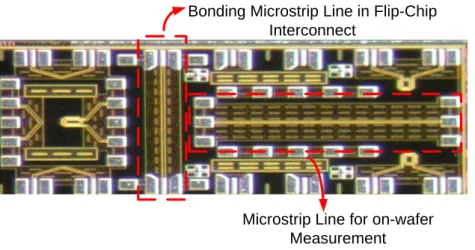
The chip micrograph is shown in Fig. 2.16, including the bonding microstrip line in flip-chip interconnect, a microstrip line for an on-wafer measurement, and other test structure.
2.3.1 Measurement Results of the Microstrip Line
The measurement results of the on-chip microstrip line are shown in Fig. 2.17. The return loss of the microstrip line is kept low over the frequency band. The insertion
Microstrip Line for on-wafer Measurement
Bonding Microstrip Line in Flip-Chip Interconnect
loss is around -0.4dB up to 50 GHz. The measurement results include the effects of the GSG test pad. This measurement results show that the line impedance of the microstrip line is closed to 50Ω and the line loss is small.
2.3.2 Measurement Results of the CPW
Multi-line de-embedding method is adopted to extract the characteristic impedance and propagation constant of the CPW. The measurement results including characteristic impedance and propagation constant are shown in Fig. 2.18 indicating that the Zo is deviated from 50Ω and more dependent on frequency than the simulation results. This is due to under-estimate the conductivity of silicon substrate. In the initial design, the substrate conductivity is set as 10 S/m. However, if the conductivity is adjusted to around 75 S/m, the simulation results agree well with the measurement results. The deviation of Zo in the CPW will cause serious effects on the TRL measurement because Zo in the measurement system is defined by the line
0 10 20 30 40 50 -38 -36 -34 -32 -30 -28 -26 -24 -22 -20 S 11& S 22 (dB ) freq (GHz) S11 S22 0 10 20 30 40 50 -0.7 -0.6 -0.5 -0.4 -0.3 -0.2 -0.1 0.0 S2 1&S1 2 (d B) freq (GHz) S21 S12 (a) (b) Fig. 2.17. Measurement results of the microstrip line: (a) return loss. (b) insertion loss.
impedance of the CPW. And the higher conductivity of silicon substrate will increase more insertion loss in the flip-chip interconnect.
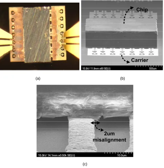
2.3.3 Measurement Results Using TRL Calibration
Fig. 2.19 shows the SEM pictures of the entire flip-chip structure and the bonding interface. The enlarged SEM picture of Fig. 2.19(c) shows 2µm misalignment in the bonding interface at the transition. It is due to the function loss of interlocking in this case since Zn/Ni/Au layers on the Al pad were over-plated to make its surface above the passivation. The issue can be further resolved with better process control.
0 10 20 30 40 50 32 36 40 44 48 52 Zo ( O hm ) freq (GHz) Measured Sim_Si 75 S/m 0 10 20 30 40 50 0 100 200 300 400 500 600 al pha ( n eper s/ m ) Freq (GHz) Measure Sim_ Si 75 S/m (a) (b) 0 10 20 30 40 50 0 500 1000 1500 2000 2500 bett a ( radia ns/m) Freq (GHz) Measure Sim_Si 75 S/m (c)
Fig. 2.20. Reference planes of the flip-chip test structure by TRL measurements and EM simulations. Carrier Chip (a) (b) 2um misalignment (c)
Fig. 2.19. Pictures of flip-chip structure. (a) on-wafer probing. (b) SEM photo of flip-chip structure. (c) Bonding interface in transition structure shows 2um misalignment.
Misalignment may cause some effects in return loss and insertion loss due to local refection in the discontinuity.
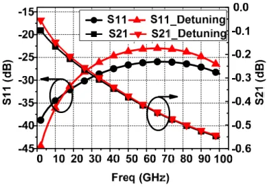
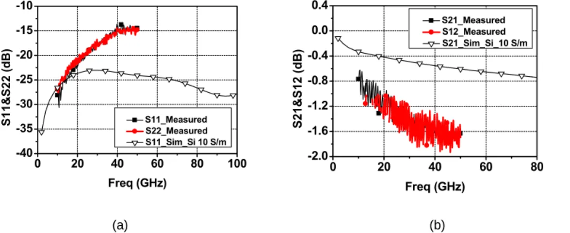
On-wafer probing measurements are conducted to characterize the electrical performance of the flip-chip test structure. The TRL calibration technique is applied to move the reference plane of measurement to the location close to the transition interface, as shown in Fig. 2.20. The chip is measured only up to 50GHz due to the equipment limit. The measured data is plotted in Fig. 2.21 showing that the flip-chip interconnects exhibits an insertion loss less than 1.7 dB and a return loss better than 15dB up to 50GHz, including the transmission loss of CPW and microstrip line. The contact resistance of the flip-chip bonding is verified by DC measurement of the test structure. It is as low as 0.7Ω including two CPW lines with the length of 200um, two contact resistances, and one THRU line on the chip. Discrepancy from the simulation results and the measurement results mainly come from the under-estimation of silicon
0 20 40 60 80 100 -40 -35 -30 -25 -20 -15 -10 S1 1&S2 2 (dB) Freq (GHz) S11_Measured S22_Measured S11_Sim_Si 10 S/m 0 20 40 60 80 -2.0 -1.6 -1.2 -0.8 -0.4 0.0 0.4 S21&S12 ( d B ) Freq (GHz) S21_Measured S12_Measured S21_Sim_Si_10 S/m (a) (b)
Fig. 2.21. Comparison between simulation and measurement data, (a) return loss and (b) insertion loss. Simulation is based on initial assumption of silicon conductivity of 10S/m.
conductivity in the carrier. The misalignment and the contact resistance in the transition interface may contribute additional insertion loss, which is not included in EM simulation.
2.3.4
Trouble Shooting
As seen in Fig. 2.21, simulation and measurement data appear different levels. After investigations, the difference might be due to two factors, process variation of CPW line and underestimation of its substrate conductivity.
(i) Process Variation
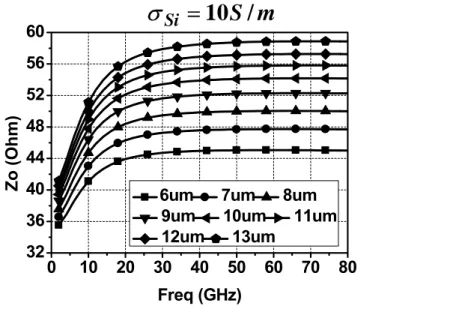
Process variation causes the CPW line width become wider as 11.7um so that the gap size changes to 6.75um which causes Zo deviate from 50Ω. Smaller gap width means higher capacitive coupling between the signal line and the ground line resulting in a lower characteristic impedance. The dependence of Zo on the frequency under
m
S
Si=
10
/
σ
0 10 20 30 40 50 60 70 80 32 36 40 44 48 52 56 60 Zo (Ohm) Freq (GHz)6um 7um 8um
9um 10um 11um
12um 13um
different gap size as signal width is fixed to 10.5um is shown in Fig. 2.22. This process variation may cause 2~3Ω variation in Zo. This small variation does not affect the return loss too much if the level of Zo is still closed to 50Ω.
(ii) Silicon Conductivity Issue
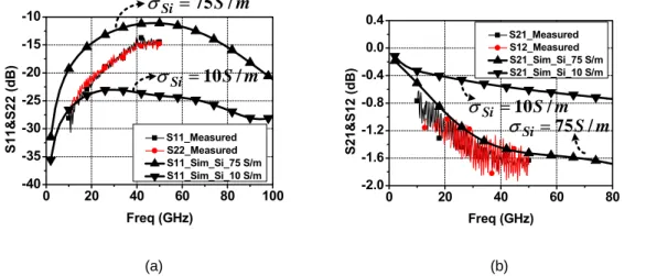
2~3Ω variation in Zo does not affect the overall response of the flip-chip interconnection very much. The main reason for the discrepancy in Fig. 2.21 is because we under-estimate the silicon conductivity. From the previous discussion of the measurement results of the CPW, the conductivity of the Si substrate is extracted as 75 S/m, much higher than the initial assumption of 10 S/m. This higher silicon conductivity will cause Zo change a lot and become more dispersive. And it also contribute more signal loss to flip-chip interconnect due to the EM fields on the lossy substrate. Zo of the measurement system in TRL calibration is set by the standard of
m S Si =75 / σ 0 20 40 60 80 100 -40 -35 -30 -25 -20 -15 -10 S1 1&S2 2 (dB) Freq (GHz) S11_Measured S22_Measured S11_Sim_Si_75 S/m S11_Sim_Si_10 S/m m S Si=10 / σ 0 20 40 60 80 -2.0 -1.6 -1.2 -0.8 -0.4 0.0 0.4 S21& S 1 2 ( d B) Freq (GHz) S21_Measured S12_Measured S21_Sim_Si_75 S/m S21_Sim_Si_10 S/m m S Si =75 / σ S m Si =10 / σ (a) (b)
Fig. 2.23. Comparison between simulation and measurement data, (a) return loss and (b) insertion loss. Simulation data with revised the CPW line dimensions and the substrate conductivity (Sx1_Sim_75 S/m Si) agree well with measurement data.
CPW line so that this higher silicon conductivity will cause the TRL measurement results worse. This is because Zo of the CPW is deviated from 50Ω very much, but Zo of the microstrip line is kept around 50Ω. Fig. 2.23 shows the revised simulation results with the silicon conductivity set to 75 S/m. Given the new dimensions and the substrate conductivity, revised simulation data of the insertion loss agree well with measured data. The return loss curves appear in a better similar trend. Nevertheless, the return loss is worse and the insertion loss is higher than the original design.
2.3.5 Measurement Result Using Multi-Line De-embedding Method
Multi-line de-embedding method is also adopted to test the transition structure. The system characteristic impedance is set to 50Ω over the signal frequency, common condition in the S-parameter measurement. The measured data is plotted in Fig. 2.24 showing that the flip-chip interconnects exhibits an insertion loss less than 3 dB and a return loss better than 16dB up to 50GHz, including the transmission loss of
0 10 20 30 40 50 -40 -35 -30 -25 -20 -15 -10 S11 (dB ) freq (GHz) Sim
Measured SimMeasured
0 10 20 30 40 50 -4 -3 -2 -1 0 S21 (dB) freq (GHz) (a) (b)
Fig. 2.24. Measurement results using multi-line de-embedding method. (a) return loss. (b) insertion loss.
CPW and microstrip line. The measured insertion loss by multi-line de-embedding method is different from that using TRL calibration. The result using TRL calibration is more reliable than that using multi-line de-embedding method because the reference plane is specifically defined to the place we desired and any non-ideal effect, such as discontinuity of pad, and any interconnects for measurement, can be removed. As for the multi-line de-embedding method, there may be a concern to make a lumped pad assumption in (2-11), especially at high frequency. And the process of calculation may contain numeric errors to impact the final results. However, using more calculation methods to characterize DUT helps understand more on the electrical properties of the flip-chip interconnect.
In other words, as to the transition structure designed in this chapter, it indeed has good broadband performance for low return loss and low insertion loss suitable for high frequency applications. This structure is easily realized without any external matching network. With good process control and accurate modeling, it is believed that the return loss could be better than 15 dB and the insertion loss could be lower than 2dB up to 100GHz, applicable to millimeter-wave circuits.
Chapter 3
A Low Power 5GHz Voltage-Controlled
Oscillator Utilizing SoP Technique
3.1 Introduction
The SoP (System-on-Package) has been attractive for RF circuit and system integration in recent years. As shown in Fig. 3.1, instead of building everything on a single chip, modules of RF transceiver components are designed and fabricated in separate chips, and then fully integrated onto a chip-carrier. Inasmuch as the implementation of high performance active and passive components without having any material and fabrication limitations, a miniaturized RF system can be realized with more design flexibility for better circuit performance.
This chapter introduces the development of a wafer-level SoP solution for 5GHz VCO using the combination of MEMS and flip-chip packaging technologies as shown in Fig. 3.2. The flip-chip interconnect has been designed and verified by the measurement as discussed in Chapter 2. The core circuit is fabricated in a standard 0.18µm CMOS process. High-performance micromachined inductors are designed, modeled, and fabricated on a silicon substrate, which also acts as a chip-carrier. Chip-carrier integration is realized by Au-Au thermal compression flip-chip bonding, introduce in chapter 3, which provides very good interconnection. On-chip circuit and on-carrier components are co-developed to achieve the required performance. More detailed information about the process and MEMS inductor can be read at [15]. The discussion in this chapter focuses on the VCO circuit design.
3.2 VCO Circuit Design
In the conventional VCO design using on-chip inductor, the VCO usually consumes larger power to compensate the high low from the LC tank. The one the benefits of using MEMS inductor is that we can design the VCO to have the same circuit
performance under lower power consumption as compared to the VCO using a low-Q inductor. This is because, as shown in Fig. 3.4, the required transconductance can be small to compensate the loss from the MEMS inductor. Besides, the MEMS inductor
m
g
/
2
−
Fig. 3.4. VCO topology using a conventional LC cross-coupled pair.
Fig. 3.3. VCO topology using a conventional LC cross-coupled pair. All CMOS transistors are to make VCO have lower flicker noise and thermal noise contributed to the phase noise.
can still have a high Q even if its inductance value is low. This property of low inductance but still high Q can make us design a width tuning range VCO under low power consumption. So we design two VCOs in this thesis to catch the two benefits discussed above.
One of the two VCOs is designed to feature in high FOM. The FOM is defined in (3-1) where P is the VCO’s core power consumption, wo is the oscillation frequency, ∆w is the offset frequency, and L(∆w) is the phase noise at the offset frequency of ∆w. The fundamental of the phase noise can be seen from Appendix A.
] ) ( 1 ) log[( 10 2 P w L w w FOM o ∆ ∆ = (3-1) The other is designed to have a high tuning range. All the power consumption of the two VCOs shall be kept low. The VCO topology used to integrate with the MEMS inductor is shown in Fig. 3.3 which is a conventional LC VCO. M1 and M2 provide the negative impedance to compensate the energy loss from the LC tank. We adopt a single switching pair to make the VCO be enable to operate at low supply voltage. Choosing PMOS topology is to have lower flicker noise and thermal noise contributing to the output phase noise [16]. M3 and M4 compose a current mirror to bias the VCO circuit. Using current mirror for the bias is to make the VCO more robust to process variation. We also add an additional Vc pad if we want to investigate the VCO performance under changes of bias current. M5 and M6 are common-source
output buffer used for the measurement purpose.
3.2.1 MEMS Inductor Design Flow
In the first place, we discuss how to design and simulate a MEMS inductor. We make use of Ansoft Designer and HFSS to layout the MENS inductor. Designer and HFSS can export the layout to a gds file. Spectre RF is for the circuit simulation. As shown in Fig. 3.5, the simulation results of inductor are exported as touch stone files (SNp files) which are import to Spectre RF by using an N-port Data item. As to the packaging issue, the package inevitably contributes some parasitic effect which should be included into the simulation. The designed flip-chip interconnect in Chapter2 shows a good return loss at 5GHz. Hence the parasitic effect of the interconnect is small such that the interconnect is likely transparent. We only need to take the contact resistance (~0.3Ω) into account to observe the degradation of Q in the MEMS inductor.
A symmetric inductor with center tap is adopted to give a higher Q and save the chip area. The required inductance value is roughly estimated according to the