Reducing Ni residues of Metal Induced Crystallization Poly-Si with a Simple Chemical Oxide Layer
Ming-Hui Lai and YewChung Sermon Wu
Department of Materials Science and Engineering, National Chiao Tung University, Hsinchu 300, Taiwan, Republic of China
The high leakage current is the most important issue of MIC-TFT. Ni residues in the MIC-TFT is the major cause of the leakage. In this study, a chemical oxide layer was used to avoid excess of Ni atoms into a-Si layer during MIC process. The process is simple and without extra thermal annealing. It was found that the Ni concentration of poly-Si film with chemical oxide layer was much less than that of conventional MIC poly-Si film. As a result, the leakage current was improved.
Introduction
Low-temperature polycrystalline silicon thin-film transistors (LTPS-TFTs) have attracted considerable interest for their use in active-matrix liquid crystal displays (AMLCD). For commercial manufacturing, Ni-metal-induced crystallization (MIC) is optimum technology of LTPS due to low cost, large area, low temperature (~500 ) and
short time for crystallization (0.5 - 5 h). However, Ni and NiSi2 residues are easy to
increase the leakage current and shift the threshold voltage [1]-[2]. Recently, several studies have demonstrated the reducing of Ni contamination; however, the on current of poly-Si films decreased [3].
In this study, a chemical oxide layer was used to avoid excess of Ni atoms into a-Si layer during MIC process. The manufacture processes were very simple and without extra thermal annealing.
Experimental
N-type self-alignment poly-Si TFTs were investigated in this study. A 100-nm-thick undoped α-Si layer was deposited onto a 500-nm-thick oxide-coated Si wafer by low pressure chemical vapor deposition (LPCVD) system. The 5-nm-thick cap oxide layer was formed by a simple chemical method [4]. A 5-nm-thick Ni film was then deposited and subsequently annealedat 500°C for 6 h in N2 to form poly-Si films. To reduce the Ni
contamination, the remained Ni film and chemical oxide layer were then removed by wet etching. The islands of poly-Si regions were defined by Reactive ion etching (RIE). Next, a 100-nm-thick gate insulator was deposited by PECVD. Then a 100-nm-thick poly-Si film was deposited as the gate electrode by LPCVD. After defining the gate, self-aligned
30 keV phosphorous ions were implanted at a dose of 5 × 1015 cm-2 to form the
source/drain and gate. Dopant activation was performed at 600°C in N2 ambient for 12 h.
It is worthy to note that manufacture processes were very simple and without extra thermal annealing. This method is very compatible with MIC processes. It just added a simple step that a-Si coated sample was immersed in chemical solution for a short time before depositing the Ni film.
ECS Transactions, 33 (5) 157-159 (2010) 10.1149/1.3481230 © The Electrochemical Society
157 ecsdl.org/site/terms_use) unless CC License in place (see abstract). address. Redistribution subject to ECS terms of use (see
140.113.38.11
RESULTS AND DISCUSSION
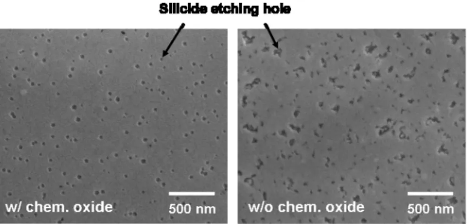
Figure 1 displays the silicide etching holes after MIC. Note that silicide-etching solutions only remove the Ni silicide not the α-Si. These holes were residues of the Ni silicides that had been etched away by a silicide-etching solution. As shown in Fig. 1, Ni concentration of poly-Si film with chemical oxide layer was much less than that of conventional MIC poly-Si film. Figure 2 shows the ID–VG transfer characteristics at a
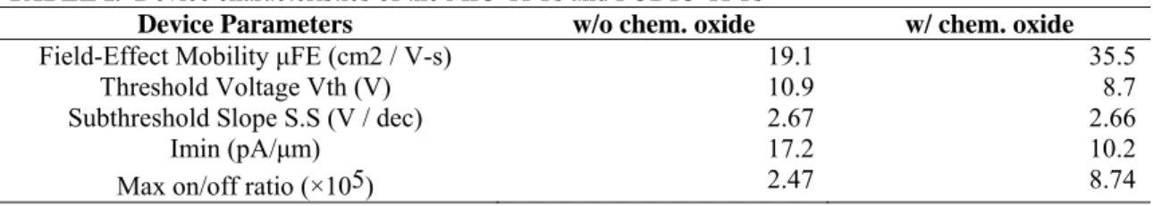
drain bias of 5 V for 10 × 10 μm2 devices. The measured and extracted key device
parameters are summarized in Table I. The threshold voltage (Vth) is defined at a
normalized drain current of IDS = (W/L) × 100nA at VDS = 5V. The field-effect mobility
(μFE) is extracted from the maximum value of transconductance at VD = 0.1V. The
electrical characters of MIC-TFTs with chemical oxide were significantly improved. It was attributed to lower Ni concentration in the MIC poly-Si films with chemical oxide layer, as shown in Fig. 1. It is known that Ni-related defects might degrade electric performance because the trap states introduced include dangling bonds and strain bonds [5]. Chemical oxide layer reduced content of Ni into channel layer during MIC annealing process to decrease Ni-related defects. Therefore, the carrier mobility increases due to lower impurity scattering of Ni-related defects.
Summary
The chemical oxide layer was used to avoid excess of Ni atoms into a-Si layer during MIC process which was very simple and without extra thermal annealing. The only extra step was immersed a-Si sample in chemical solution before depositing the Ni film. The electrical performance of MIC-TFTs with chemical oxide layer was significantly improved. It was attributed to lower nickel concentration in the MIC poly-Si films with chemical oxide layer.
Fig. 1 The silicide etching holes after metal induced crystallization of poly-Si with and without chemical oxide layer.
ECS Transactions, 33 (5) 157-159 (2010)
158 ecsdl.org/site/terms_use) unless CC License in place (see abstract). address. Redistribution subject to ECS terms of use (see
140.113.38.11
Fig. 2 Typical IDS-VGS transfer characteristics and
filed-effect mobility.
TABLE I. Device characteristics of the MIC-TFTs and FODIC-TFTs
Device Parameters w/o chem. oxide w/ chem. oxide
Field-Effect Mobility μFE (cm2 / V-s) 19.1 35.5
Threshold Voltage Vth (V) 10.9 8.7
Subthreshold Slope S.S (V / dec) 2.67 2.66
Imin (pA/μm) 17.2 10.2
Max on/off ratio (×105) 2.47 8.74
Acknowledgments
This project was funded by Sino American Silicon Products Incorporation and the NSC of the ROC under Grant No. 98-2221-E-009-041-MY3. Technical supports from the National Nano Device Laboratory, Center for Nano Science and Technology and the Nano Facility Center of the National Chiao Tung University are also acknowledged.
References
1. P. J. van der Zaag, M. A. Verheijen, S. Y. Yoon, and N. D. Young, Appl. Phys.
Lett., 81, 3404 (2002).
2. G. A. Bhat, H. S. Kwok, and M. Wong, Solid State Electron., 44, 1321 (2000). 3. C. M. Hu, Y. C. Sermon Wu and C. C. Lin, IEEE Electron Device Lett., 28, 1000
(2007).
4. B. M. Wang and Y. C. Sermon Wu, Electrochem. Solid-State Lett., 12, J14 (2009). 5. C. P. Chang and Y. C. Sermon Wu, IEEE Electron Device Lett., 30, 130 (2009).
ECS Transactions, 33 (5) 157-159 (2010)
159 ecsdl.org/site/terms_use) unless CC License in place (see abstract). address. Redistribution subject to ECS terms of use (see
140.113.38.11