行政院國家科學委員會補助專題研究計畫
□ 成 果 報 告
■期中進度報告
奈米世代 MOSFET 關鍵製程技術之研發(2/3)
計畫類別:■ 個別型計畫 □ 整合型計畫
計畫編號:NSC 92-2215-E-009-025
執行期間:92 年 08 月 01 日至 93 年 07 月 31 日
計畫主持人:羅正忠
共同主持人:葉清發
計畫參與人員: 陳永裕、陳添富、蕭智文、王碩晟。
成果報告類型(依經費核定清單規定繳交):■精簡報告 □完整報告
本成果報告包括以下應繳交之附件:
□赴國外出差或研習心得報告一份
□赴大陸地區出差或研習心得報告一份
□出席國際學術會議心得報告及發表之論文各一份
□國際合作研究計畫國外研究報告書一份
處理方式:除產學合作研究計畫、提升產業技術及人才培育研究計畫、
列管計畫及下列情形者外,得立即公開查詢
□涉及專利或其他智慧財產權,□一年□二年後可公開查詢
執行單位: 交通大學電子工程研究所
中 華 民 國 93 年 07 月 13 日
中文摘要 近年來,以氧化鋁為主的高介電材料已經逐漸取代傳統的閘極二氧化矽層,原因在於 氧化鋁跟複晶矽閘極的相容性很高,且熱穩定性及微縮能力也很傑出。在計畫的第二年, 我們研究以氧化鋁作為電晶體的閘極絕緣層,並使用快速熱退火技術來改善薄膜的電性與 降低熱預算。此外,在進行後續熱處理的過程當中,矽跟高介電材料之間很容易成長出原 生氧化層,因而大幅提高介電層的等效氧化層厚度,為了解決這個問題,我們也嘗試在沈 積氧化鋁之前,先將矽基板表面以800 度 1 小時的氨氣處理來抑制原生氧化層的成長。 在氧氣環境下的快速熱退火處理能夠有效地降低閘極漏電流,也會促進介面氧化層的 成長,相對地,氮氣熱退火處理能夠填補氧化鋁薄膜內的斷鍵,並小幅降低表面粗糙度, 此外,氨氣表面處理可以有效提高高介電氧化鋁薄膜的可靠度,藉著等效能障高度的提升, 閘極漏電流也可以明顯地降低。 此外,我們接續第一年的成果,針對無塵室內來自空氣濾網當中的硼污染進行研究, 目前使用的高效率空氣濾網多由玻璃纖維所製造,當它們在長時間使用下遭遇到氫氟酸的 侵蝕時,就會放出硼離子,進而造成奈米元件的特性漂移。利用長時間之 HF 蒸氣的加速 實驗和晶圓暴露實驗,輔以TDS-APIMS 和 SIMS 量測,即可觀察到包括各種有機分子團和 硼離子在HF 蒸氣下的增加情況,又使用 PTFE 材質的空氣濾網則能夠有效地防止硼污染。 Abstract
Recently, MOSFETs with high-k gate dielectrics have been studied intensively and Al2O3 is
a promising candidate because of its compatibility with the poly-Si gate process and relatively superior scalability. In the second year of this proposal, we utilized rapid thermal annealing technique to improve the quality of high-k film and reduce the thermal budget. Besides, a native oxide layer would easily formed at Si/Al2O3 interface during RTA process, resulting in significant
increase of effective oxide thickness (EOT) and therefore we applied a NH3 treatment at 800
degree C for 1 hr prior to Al2O3 deposition to suppress the growth of native oxide layer.
From the experimental data, it is obviously that O2 penetration would induce the increase of
the interfacial layer during RTA process. However, for samples with RTA in a N2 ambient, the
void-defect of sputtered Al2O3 film would be eliminated and the surface roughness after
annealing also reduced. The dielectric reliability was enhanced with NH3 pre-treatment. The
conduction mechanism in Al2O3 thin film is dominated by Schottky conduction which occurred in
the insulators with fewer defects and a more perfect metal-insulator interface. Samples after NH3
treatment have higher barrier high to reduce the gate leakage current.
Besides, following the results of this proposal in the 1st year, we investigated the possible boron contamination from various HEPA and ULPA filters. Most commercial ULPA filters are made of glass-fiber, which may corrode in an acid vapor environment and release boron ions, resulting in the electrical property shifts of nano-devices. Through long term acceleration experiments and wafer exposure experiments in an bench with HF vapor, the increase of organic molecular and boron ions due to filter corrosion can be observed. The usage of PTFE ULPA filter can effectively prevent the boron contamination.
I. Introduction
Recently, MOSFETs with high-k gate dielectricshave been studied intensively and Al2O3 is
a promising candidate because of its compatibility with the poly-silicon gate process and relatively superior scalability. As the dielectric constant of Al2O3 is higher than SiO2, it will
provide a significant increase in capacitance without scaling down the oxide thickness. Rapid thermal Annealing (RTA) is a short time processing technique that can contribute to reduce the thermal budget, low levels of surface roughness, and improve film qualities. Generally, there are many methods to passivate the Si surface such as surface nitridation, nitrogen-contained ambient annealing, or nitride deposition as the bottom layer. Nitridation of the Si surface using NH3
treatment before the deposition of high-k materials has been shown to be effective in achieving the low EOT and preventing the boron penetration. However, this technique results in higher interface charges, which leads to higher hysteresis and reduced channel mobility. In this report, we studied the effect of suppressing interfacial layer growth by NH3 surface treatments. The NH3
treatmentwould nitridize the Si surface to form a silicon nitride layer. Silicon nitride is a superior barrier for H2O and oxygen, and it can suppress oxygen to diffuse into Si substrate.
The cleanness of a clean room environment must be tightly controlled to achieve high-yield and high-performance ULSI manufacturing. Recently developed filters, such as HEPA and ULPA filters, effectively eliminate traditional contamination. However, the controllability of airborne molecular contamination (AMC) using present cleanroom technologies has not yet been validated because AMC is a kind of atomic or molecular level gas-phase contamination like organic and inorganic ones. In the near future, especially in the nanodevice era, contamination by organic compounds, inorganic ions and trace doping impurities in air in a cleanroom may dominate the characteristics, reliability, and even yield of devices. Acid vapor generated from the cleaning process is another important issue. Most commercial ULPA filters are made of glass-fiber, which may corroded in an acid vapor environment. Contaminants in a ULPA filter corroded by acid vapor will be released into the cleanroom air and adsorbed onto the surface of wafers, degrading the manufactured devices. Technologies for eliminating AMC from the manufacturing environment must be developed to solve these problems completely. Therefore, the development of a new filter material, which has minimal AMC and is resistant to acid vapor corrosion, is important to the fabrication of high-performance devices.
II. Experiments
(A) Al2O3 Gate Dielectrics Using Rapid Thermal Annealing Technology
The 6-inch P-type Si (100) wafers are cleaned by the RCA cleaning process. The high-k material Al2O3 was then deposited by reactive sputtering in Ar/O ambient. After Al2O3 deposition,
a high temperature post deposition annealing is performed at 750 ℃ , 850 ℃ and 950 ℃ respectively for 30 sec by RTA Rapid Thermal Annealing (RTA). In our experiment, the gate electrode formations were used the Physical Vapor Deposition (PVD) systems. We deposit the TiN film (2000Å ) as the top gate electrode and the thermal evaporation system to deposit the Al film( 5000Å ) as the backside contact. The cross-sectional view and total experimental procedures of the structure were shown in Fig. 1. At last the Capacitance-Voltage (C-V) and Current-Voltage (I-V) characteristics were measured by HP-4284 and HP-4156C systems. The capacitance equivalent thickness (CET) was extracted from C-V curve.
(B) Al2O3 Gate Dielectrics using NH3 Surface Nitridation Technology
First, the 6-inch P-type Si(100) wafers were cleaned with standard RCA clean. The samples were divided into two groups. One was without any surface treatment before Al2O3 deposition,
and the other was with a NH3 surface treatment before Al2O3 deposition. The NH3-treatment is
performed in high temperature furnace, 800℃ for 1 hour. After NH3-treatment, a SiNX layer(~10
Å) was deposited. Al2O3 dielectric was then deposited various thickness (30Å, 40Å, and 50Å) by
reactive sputtering in the Ar/O (ratio = 24/1) ambient. After Al2O3 deposition, a high temperature
post deposition annealing was performed at 900℃ in the O2 or N2 ambient. Finally, the gate
electrode formation was performed by the Physical Vapor Deposition (PVD) systems. We deposited the TiN film (2000Å ) as the top gate electrode and the thermal evaporation system to deposit the Al film ( 5000Å ) as the backside contact. The cross-sectional view and total process flow were shown in Fig. 10. The Capacitance-Voltage (C-V) and Current-Voltage (I-V) characteristics were measured by HP-4284 and HP-4156C systems, respectively. The capacitance equivalent thickness (CET) was extracted from C-V curve. In order to study the conduction mechanism in the Al2O3 film, the current-voltage characteristics with various temperature were
measured at room temperature (RT), 50℃, 75℃, 100℃, and 125℃, respectively.
(C) Evaluation of AMC through Air Sampling
A specially controlled and fabricated clean bench (CB) was set up in a clean room of class 10k. Figure 19(a) schematically depicts the CB. Clean room air, from the air inlet of the CB, was initially filtered through a filter module that included inorganic and organic ion chemical filters, before flowing through the main filter, which was designed to be changeable. Two main filters were used, the NEUROFINE PTFE filter (PTFE) and the glass-fiber ULPA filter (GF). The air flow rate and turnover rate inside the CB were set to 0.4 m/s and 5 %, respectively. The exposure experiments were conducted in a 1ppm HF vapor environment.
Figure 19(b) presents the air sampling tools, Impinger and TENAX, which were equipped with a flow meter and a pump. The flow rate and sampling time of Impinger were 2 L/min and 24-72 hrs while those of TENAX were 100 mL/min and 5 hrs. Impingers collected mainly both metals and boron elements. These were analyzed using an inductively coupled plasma mass spectrometer (ICP-MS). Organic substances were collected by a TENAX (a kind of absorbent) tube, and quantitatively analyzed by gas chromatograph mass spectrometer (GC-MS). The air in the CR was also analyzed for comparison. Table 2 summarizes the air sampling experimental conditions.
(D) Evaluation of AMC through Wafer Sampling
The AMC absorbed on the surfaces of actual 6” P-type (100) Si wafers was analyzed for each filter module. After standard RCA cleaning, wafers were divided into two parts, and exposed to the air in the CR and the CB for 24-72 hrs. The metal contaminants on these wafer surfaces were analyzed using total reflection X-ray fluorescence (TRXRF), while the organic contaminants were analyzed by thermal desorption system–atmospheric pressure ionized mass spectrum (TDS-APIMS). For comparison, the contamination of a wafer not exposed to any environment was evaluated as a control. Table 3 is the summary of wafer sampling experimental conditions.
III. Results and Discussion
(A) Al2O3 Gate Dielectrics Using Rapid Thermal Annealing Technology
After the Al2O3 deposition, the following processes may go through many high temperature
treatments during the VLSI fabrication. Such high-temperature treatments are likely to change the morphology and properties of thin films. Fig. 2 and Fig. 3 shows the high frequency (100kHz) capacitance-voltage (C-V), and Fig. 4 shows the CET of Al2O3 samples (without surface
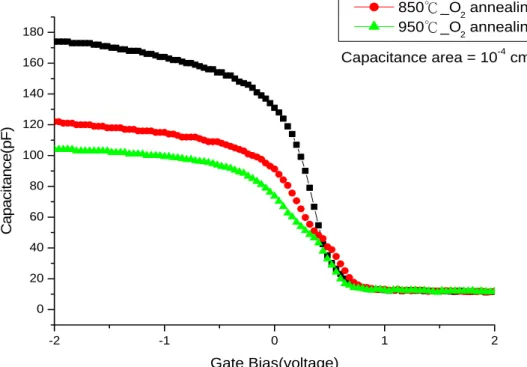
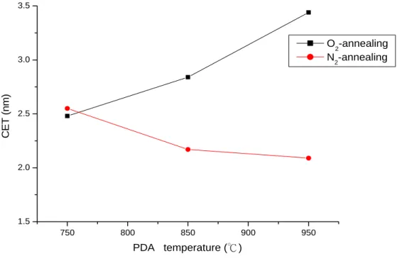
treatment) after various post deposition annealing (PDA) temperature at 750℃, 850℃, 950℃ in the O2 or N2 ambient. The capacitance of Al2O3 samples annealing in an O2 ambient decreases
with the increasing annealing temperature. Therefore, the CET increases after annealing in an O2
ambient. This is because an O2 penetration will induce the increasing of the interfacial layer at
Al2O3/Si-substrate and higher annealing temperature increasing will speed up interface layer
growth rate. On the contrary, the capacitance of Al2O3 samples annealing in a N2 ambient is
increasing when annealing temperature increases. Therefore, the CET decreases after annealing in a N2 ambient. The void-defects generated after the sputtered Al2O3 formation and it could be
densified followed a RTA process in a N2 ambient. The current density (J) in the J-E curve was
defined by J = I / A, where A is the area of capacitor. The CET determined by the C-V measurement.
Fig. 5 shows the J-E characteristics of Al2O3 film with RTA process in an O2 ambient. It
shows that the thicker Al2O3 film will resist large leakage current, and the lower leakage current
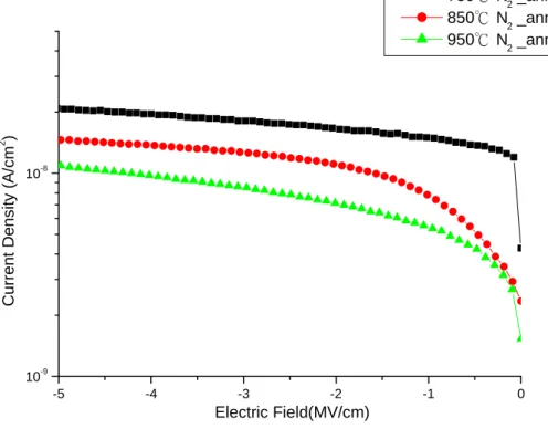
was observed. However, the thicker dielectric thickness will reduce capacitance and the driving current. Fig. 6 shows the J-V characteristics of the fabricated Al2O3 film with RTA in a N2
ambient. The capacitor can have a lower leakage current with thinner CET. This is due to RTA process in a N2 ambient can improve Al2O3 film by eliminating void-defect. Fig. 7 shows J versus
PDA temperature in the O2 and N2 ambient. Obviously, higher PDA temperature can reduce
leakage for both annealing ambient. Consequentially, the sputtered Al2O3 film can be improved
after a N2 RTA process. If the leakage current density in the oxide (Jox) is kept constant during
the stress test (implying that the applied current is held constant), the stress time to breakdown becomes the variable. The length of stress time tBD elapsed until dielectric breakdown occurred.
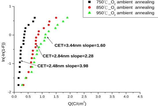
The time-to-breakdown behavior of a group of oxide samples under such test conditions is referred to as time-dependent dielectric breakdown (TDDB). The Weibull plot of charge to breakdown for Al2O3 samples with various PDA temperature in an O2 ambient is shown in Fig. 8.
Obviously, distribution of the samples with thinner CET is better than others. However, the level of the charge to breakdown is lower than we expect. Fig. 9 shows the Weibull plot of charge to breakdown for Al2O3 samples with various PDA temperature in a N2 ambient. For various PDA
temperatures, their distribution and charge to breakdown are almost the same and they are not dependent on Al2O3 thickness. This means that the interfacial layer determines the breakdown of
the whole stack.
(B) Al2O3 Gate Dielectrics Using NH3 Surface Nitridation Technology
Figure 11 shows the comparisons of the C-V curves of the samples with and without surface treatment after PDA 900℃ in an O2 ambient. It is clear that samples with a NH3 treatment had
higher capacitance at strong accumulation than samples without a NH3 treatment. The CET of
of interfacial layer. In Fig. 11, we can also found the C-V curves shift negatively after NH3
nitridation can be observed due to the nitridation-induced fixed positive charges. Since positive fixed charges in conventional NH3 nitridation film is due to N–H bonds at the interface. Fig. 12
shows the comparisons of the C-V curves of the samples with or without surface treatment after PDA 900℃in a N2 ambient. We still can find that the CET of Al2O3 filmis effectively reduced
after NH3 treatment. However, the amount of the C-V curves shift negatively after NH3 nitridation is decreasing. The reason is due to that PDA in a N2 ambient will enhance the
magnitude of fixed charge in Al2O3 film Fig. 13 shows the variation of deposited thickness
(measured by ellipsometer ) versus CET after PDA 900℃in an O2 ambient. The NH3 treatment
can effectively reduce the CET despite the initial oxide thickness, which shows the excellent CET scalability of this nitridation process. Because the presence of Si3N4 layer can effectively
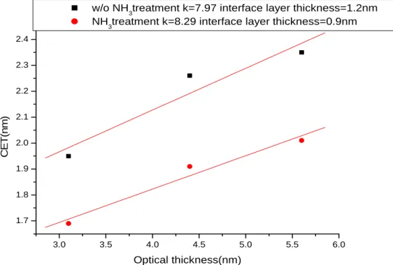
suppress the diffusion of oxygen species into the high-k/Si substrate interface. Without surface nitridation, Al and O atoms are easier to react with Si and are likely to form additional silicon dioxide and/or aluminum silicate layer with relatively lower k value. Fig. 14 shows the variation of Al2O3 thickness versus capacitance equivalent thickness (CET) after PDA 900℃ in a N2
ambient. We can see almost the same result in an O2 ambient as in a N2 ambient, except in a N2
ambient with higher k value. Figure 15 (a) and (b) show the relationship of gate leakage current versus gate bias after PDA 900℃ in the O2 and N2 ambient, respectively. The NH3 –treatment
samples show lower leakage current even with thinner CET. It is postulated that the NH3-treatment can improve the quality of interface between high-k and silicon substrate and
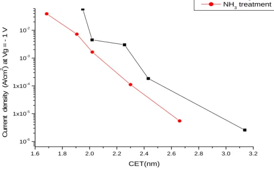
effectively reduce the leakage current. Fig. 16 shows the curve of Current density versus CET curves at Vg = -1V with NH3 treatment and without NH3 treatment. It is clear that NH3 treatment
can effectively reduce leakage current. Fig. 17(a) and (b) show the Weibull plots of the charge to breakdown (QBD) of Al2O3 samples with nearly the same CET after PDA 900℃ in theO2 and N2
ambient, respectively. The samples with NH3 treatment shows more charge to breakdown (QBD).
Thus, we suspect that surface nitridation may effectively reduce the concentration of oxygen vacancies during PDA due to its capability to suppress oxygen diffusion. On the other hand, the stronger Si-N bonds bring a stronger interface layer. When part of voltage drop across the Si3N4
interfacial layer in samples, the voltage drop across the Al2O3 film is lower than expectance and
the influence of the electric field stress is not as severe as the un-NH3 treatment Al2O3 samples.
As the result, it will enhance the QBD for NH3 treated Al2O3 samples.
It is important to study the conduction mechanisms of leakage current in Al2O3 film to
improve its electrical and dielectric properties. Typically, two possible effects are in the metal-insulator interface, one is Schottky effect, the other is Frenkel-Poole effect. The Schottky-Richardson emission generated by the thermionic effect is caused by the electron transport across the potential energy barrier via field-assisted lowering at a metal-insulator interface. The leakage current equation is:
⎟ ⎟ ⎠ ⎞ ⎜ ⎜ ⎝ ⎛ − = T k E T A J B s s φ β 12 2 * exp where 2 1 0 3/4 ) ( πε ε
βs = e , A* effective Richardson constant,φ
can find the slope of the leakage current equation. T k slope T k T A E T k J B s B s B s β φ β = ⎥ ⎦ ⎤ ⎢ ⎣ ⎡ − + = ln( ) ln * 2
The Frenkel- Poole (F-P) emission is due to field-enhanced thermal excitation of trapped electrons in the insulator into the conduction band. The leakage current equation is:
⎟
⎟
⎠
⎞
⎜
⎜
⎝
⎛
−
=
T
k
E
J
J
B PF FPφ
β
12 0exp
where J0 =σ0E is the low-field current density, σ0 the low-field conductivity, 2
1 0 3
FP
=
(
e
/
πε
ε
)
β
,e the electronic charge,ε0 the permittivity of free space,ε the high
frequency relative dielectric constant, T absolute temperature ,E the applied electric filed, KB the
Boltzmann constant,φPF the contact potential barrier. We can find the slope of the leakage current
equation. T k slope T k J E T k J B FP B PF B FP β φ β = ⎥ ⎦ ⎤ ⎢ ⎣ ⎡ − + = ln( ) ln 0
From the equations as shown above, leakage current behaviors of insulate films can be investigated further on the leakage current density (J)-electric field (E) characteristics such as ln J vs. E1/2 plots. The plot of the nature log of leakage current density versus the square root of the applied electric field was observed. It is found that the leakage current density is linearly related to square root of the applied electric field. The linear variations of the current correspond either to Schottky emission or to Frenkel-Poole conduction mechanism. For trap states with Coulomb potentials, the expression is virtually identical to that of the Schottky emission. The barrier height,
however, is the depth of the trap potential well, and the quantity β is larger than in the case of FP
Schottky emission by a factor of 2. Distinction between the two processes can be done by comparing the theoretical value of β with the experimental one obtained by calculating the slope of the curve ln J-E1/2. The dielectric constant of Al
2O3 is 7.63 at PDA O2 ambient and 8.29 at
PDA N2 ambient extracted by Fig. 20, the theory β values are 4.40×10⁻²³ for Frenkel-Poole and
2.20×10⁻²³ for Schottky after PDA in an O2 ambient and the theory β values are 4.22×10⁻²³ for
Frenkel-Poole and 2.11×10⁻²³ for Schottky after PDA in a N2 ambient. Table 1 (a) and (b) shown
the experimental β and Schottky barrier high of Al2O3 samples with NH3 and without NH3
treatment after PDA 900℃in an O2 ambient and after PDA 900℃in a N2 ambient, respectively.
Fig. 18 (a) and (b) show the conduction mechanism fitting of Al2O3 samples with NH3 and w/o
NH3 treatment after PDA 900℃in an O2 ambient and after PDA 900℃ in a N2 ambient,
conduction.
(C) Pre- and Post-corroded Fiber Structure in HF Vapor Environment
Figure 20 shows the fiber structure of PTFE-fiber and glass-fiber after the HF vapor corrosion. The pre- and post-corroded fiber structure of PTFE did not reveal any difference and this meant the PTFE-fiber was resistive for HF vapor. On the contrary, the fiber structure of glass-fiber shown in Fig. 20(b) displayed the serious degradation in HF vapor environment. The glass-fiber was inevitable to be corroded due to the strong reduction of HF to glass. It is worthy to notice that the corrosion of glass-fiber may release the boron and organic contaminants contained in glass-fiber ULPA filter, thus causing the degradation of device characteristics. Therefore, the PTFE ULPA filter is suitable to be used in acid vapor environment.
(D) Air Sampling Results in HF Vapor Environment
Figure 21 is the ICP-MS analysis results of metals and boron for different filter modules in HF vapor environment. The PTFE and the glass-fiber ULPA filter can effectively filter the metals including Na, K, Ca, Mg and Al. The CB with the PTFE and the GF ULPA filter, however, showed higher concentration of Fe ions than CR. It was suggested that the steel construction of clean bench corroded by HF vapor, releasing the Fe ions to air. Besides, the CB with GF filter showed large concentration of boron than the CB with PTFE filter. This may due to the corrosion of glass-fiber in HF vapor, releasing the boron atoms contained in glass-fiber as mentioned above. The detail analysis results of ICP-MS are listed in Table 4.
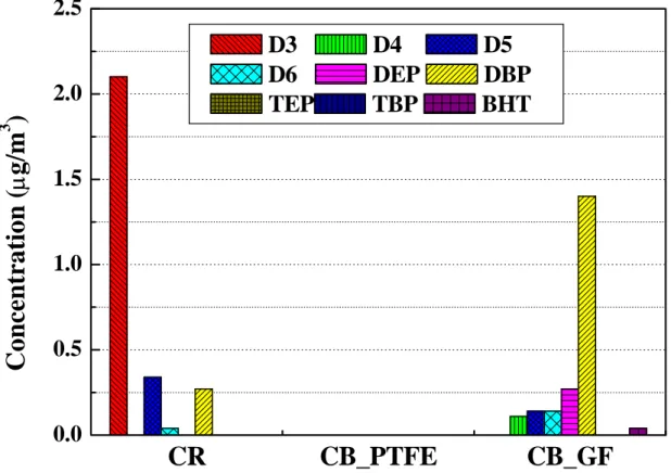
The organic compounds were considered to be another contamination the glass-fiber will release in HF vapor. Figure 22 shows the analysis results of GC/MS. It was found that all the organic contaminants were removed in the CB with PTFE filter. But for the CB with GF filter, high concentration of organic contaminants appeared. According to our study in Chapter 2, these organic contaminants may come from the binder in GF ULPA filter. In HF vapor environment, the degradation of glass-fiber will release more organic contaminants as show in Fig. 22. Table 5 shows the detail analysis results of GC/MS.
IV. Conclusion
In this thesis, characteristics and reliability of Al2O3 gate dielectrics with pre-deposition
NH3 treatment and rapid thermal annealing in O2 and N2 ambient have been investigated. Several
important phenomena were observed and summarized as follows. PDA can effectively reduce leakage current. For the samples with PDA at O2 ambient, the interfacial layer increases with the
higher PDA temperature. It is obviously that O2 penetration will induce the increasing of the
interfacial layer at Al2O3/Si-substrate and higher annealing temperature will speed up interface
layer growth rate. For samples with PDA in a N2 ambient, the void–defect of sputtered Al2O3 film
will be eliminated. The as deposited Al2O3 film shows larger roughness, and after PDA it will
become smoother. However, with higher PDA temperature, surface rough will slightly increase. The surface NH3 treatment can lower the CET value and reduce the leakage current. In
addition, the dielectric reliability was enhanced with NH3 treatment. The low Weibull slope of
Al2O3 film may result from sputter-induced defects causing weak spots. Significant process
improvements are necessary to enhance dielectric quality, such as MOCVD, ALCVD. The conduction mechanism in Al2O3 film was investigated by the various temperature measurement
and fitting. The conduction mechanism in Al2O3 thin film is dominated by Schottky conduction
which occurred for insulators with fewer defects and a more perfect metal-insulator interface. Samples after NH3 treatment will have higher barrier high to reduce the leakage current.
The qualitative and quantitative analyses of AMC in the CB with different filter module in HF vapor environment were investigated. The experimental results showed that the GF ULPA filter will release boron and organic contaminants in HF vapor environment, while the PTFE ULPA filter still maintained low concentration of contaminants. The effects of the materials from which air filters are made on device characteristics were also investigated. The glass-fiber ULPA filter released AMC when exposed in an HF vapor environment. These contaminants included organic compounds and boron trace dopants and degraded the device characteristics. In contrast, the HF vapor did not affect the PTFE ULPA filter. These results suggested that the PTFE fiber can be a good ULPA filter material for providing a very clean environment.
計畫成果自評 本計畫為三年期計畫,依原訂計畫第二年目標,本計畫完成了奈米級閘極介電層關鍵製程 技術之研發以及奈米級微污染分析防治,相關論文仍在投稿當中。在奈米級閘極介電層關 鍵製程技術之研發方面,開發出未來奈米元件用之高介電常數 Al2O3閘極介電層,並研究 其特性及最佳化條件,此高介電氧化鋁薄膜經過NH3的前處理及N2 RTA 製程退火處理, 可獲得最佳電性,適用於未來的奈米元件製程;最後在奈米級微污染分析防治方面,我們 以氫氟酸加速實驗檢驗了目前無塵室空氣濾網的適用性,並採用新開發之 PTFE 濾網來控 制無塵室中之硼微污染跟有機污染。本計畫未來一年將以前兩年為基礎,繼續進行氧化鋁 和臭氧水製程之奈米閘極絕緣層跟無塵室微污染對於奈米元件之影響等相關研究。
1
. RCA clean and LOCOS Si-SubstrateSi-Substrate Al2O3
3
. RTA treatment N2/ 5 slm/30 sec orO2/ 5 slm/30 sec 750℃ 850 , ℃ ,950℃
2
. Al2O3 deposition ( 60Å )by Reactive Sputter
4
. Top electrode formation TiN-2000 Å & Backside contact formation Al -5000ÅAl2O3
Si-Substrate
TiN
Al2O3
Si-Substrat
Fig.1 Process flows of experimental samples Al
-2 -1 0 1 2 0 20 40 60 80 100 120 140 160 180 Capacitance area = 10-4 cm2 C apac it ance( pF) Gate Bias(voltage) 750℃_O2 annealing 850℃_O2 annealing 950℃_O2 annealing -2 -1 0 1 2 0 20 40 60 80 100 120 140 160 180 200 750℃_N2 annealing 850℃_N2 annealing 950℃_N2 annealing Capacitance area = 10-4 cm2 Gate Bias(voltage) Capacitan ce(pF)
Fig.2 The C-V curves of Al2O3 samples annealing in an O2 ambient
750 800 850 900 950 1.5 2.0 2.5 3.0 3.5 O 2-annealing N 2-annealing CE T ( n m) PDA temperature (℃) -4 -3 -2 -1 0 10-8 750℃_O2 annealing 850℃_O2 annealing 950℃_O2 annealing Cur rent De nsit y ( A /c m 2 ) Electric Field(MV/cm)
Fig. 4 The CET of Al2O3 samples after various post annealing temperature
750℃, 850℃,950℃
Fig. 5 The J-E curves of Al2O3 samples with various PDA temperature in an O2
-5 -4 -3 -2 -1 0 10-9 10-8 C u rr ent Density (A /cm 2 ) Electric Field(MV/cm) 750℃ N2 _annealing 850℃ N2 _annealing 950℃ N2 _annealing 750 800 850 900 950 1.0x10⁻⁸ 1.2x10⁻⁸ 1.4x10⁻⁸ 1.6x10⁻⁸ 1.8x10⁻⁸ 2.0x10⁻⁸ 2.2x10⁻⁸ 2.4x10⁻⁸ J(A /cm 2 ) @ V g = -1V PDA temperture( ℃ ) O2ambient annealing N 2ambient annealing
Fig. 7 The J at Vg= -1 V of Al2O3 samples with various PDA temperature
Fig. 6 The J-E curves of Al2O3 samples with various PDA temperature in a N2
0.0 0.5 1.0 1.5 2.0 2.5 3.0 3.5 4.0 4.5 -2 -1 0 1 CET=3.44nm slope=1.60 CET=2.84nm slope=2.28 CET=2.48nm slope=3.98 ln (-l n (1 -F )) Q(C/cm2) 750℃_O 2 ambient annealing 850℃_O2 ambient annealing 950℃_O2 ambient annealing 0 1 2 3 4 5 6 7 8 9 -3 -2 -1 0 1 750℃_N 2 ambient annealing 850℃_N2 ambient annealing 950℃_N2 ambient annealing CET=2.09nm slope=0.63 CET=2.17nm slope=0.62 CET=2.55nm slope=0.57 ln(-ln(1-F)) Q(C/cm2)
Fig. 9 The Weibull plot shows the charge to breakdown Q (C/cm2) of Al2O3
samples with various PDA temperature in a N2 ambient.
Fig. 8 The Weibull plot versus the charge to breakdown Q (C/cm2) of Al2O3
‘
1
. RCA clean Si-Substrate2
. Without treatment Si-Substrate Si-Substrate2
. NH3 1hr 800℃ treatment Si-Substrate Al2O3 Si-Substrate Al2O33
. Al2O3 deposition( 30,40,50Å ) SiNX4
. RTA treatment N2/ 5 slm/ 30sec orSi-Substrate Al2O3
3
. Al2O3 deposition( 30,40,50Å )Si-Substrate
5
. Top electrode formation TiN -2000 Å pattern contact Al2O3 TiN SiNX Al2O3 Si-Substrate TiN Al2O3 Si-SubstrateFig.10 Process flows of experimental samples Si-Substrate
SiNX
SiNX
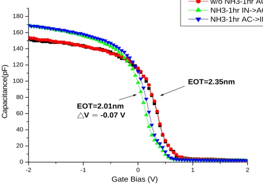
-2 -1 0 1 2 0 20 40 60 80 100 120 140 EOT=3.14nm EOT=2.66nm △V = -0.04 V w/o NH3-1hr IN->AC w/o NH3-1hr AC->IN NH3-1hr IN->AC NH3-1hr AC->IN Gate Bias (V) C a paci ta n c e (p F) -2 -1 0 1 2 0 20 40 60 80 100 120 140 160 180 EOT=2.01nm △V = -0.07 V EOT=2.35nm Gate Bias (V) C apa ci ta nce (p F ) w/o NH3-1hr IN->AC w/o NH3-1hr AC->IN NH3-1hr IN->AC NH3-1hr AC->IN
Fig. 11: C-V curve of Al2O3 sample with surface treatment compare to Al2O3 sample
without surface treatment after PDA 900℃in an O2 ambient
Fig. 12: C-V curve of Al2O3 sample with surface treatment compare to Al2O3 sample
3.0 3.5 4.0 4.5 5.0 5.5 6.0 1.6 1.8 2.0 2.2 2.4 2.6 2.8 3.0 3.2 CET (nm ) Optical thickness(nm)
w/o NH3treatment k=6.56 interface layer thickness=1.4nm
NH3treatment k=7.63 interface layer thickness=1.1nm
3.0 3.5 4.0 4.5 5.0 5.5 6.0 1.7 1.8 1.9 2.0 2.1 2.2 2.3 2.4 w/o NH
3treatment k=7.97 interface layer thickness=1.2nm
NH
3treatment k=8.29 interface layer thickness=0.9nm
CET
(n
m
)
Optical thickness(nm)
Fig. 14: CET versus Optical thickness of Al2O3 sample with surface treatment compare to
Al2O3 sample without surface treatment after PDA 900℃in a N2 ambient
Fig. 13: CET versus Optical thickness of Al2O3 sample with surface treatment compare to
-4 -2 0 10-7 10-6 1x10⁻⁵ 1x10⁻⁴ 10-3 10-2 C u rre n t D e n s it y (A /c m 2 ) Electric Field(MV/cm) w/o NH3treatment NH3 treatment -4 -2 0 10-8 10-7 10-6 1x10⁻⁵ 1x10⁻⁴ 10-3 10-2 10-1 w/o NH3treatment NH3 treatment C u rre n t D e n s it y (A /c m 2 ) Electric Field(MV/cm)
Fig. 15(a): The gate leakage current density (J) versus electric field (E) curves for NH3
nitrided and w/o NH3 nitrided after PDA 900℃in an O2 ambient
Fig. 15(b): The gate leakage current density (J) versus electric field (E) curves for NH3
1.6 1.8 2.0 2.2 2.4 2.6 2.8 3.0 3.2 10-6 1x10⁻⁵ 1x10⁻⁴ 10-3 10-2 C u rr e n t d e n s ity ( A /c m 2 ) a t V g = - 1 V CET(nm) w/o NH3 treatment NH3 treatment 0 2 4 6 8 10 12 14 16 -2.0 -1.5 -1.0 -0.5 0.0 0.5 1.0 CET=2.30nm CET=2.43nm CET=2.02nm CET=2.09nm ln (-ln (1 -F )) QBD(C/cm2)
w/o NH3 treatment slope=1.67927 w/o NH3 treatment slope=1.21684 NH3 treatment slope=1.1456 NH3 treatment slope=0.76316
Fig. 17 (a)The weibull plot shows charge to breakdown for Al2O3 samples with NH3
and w/o NH3 treatment at PDA after PDA 900℃in an O2 ambient
Fig. 16 Current density at Vg = -1Vversus CET curves for NH3 treatment and
2 4 6 8 10 12 14 16 18 20 22 24 26 28 -2.5 -2.0 -1.5 -1.0 -0.5 0.0 0.5 1.0 CET=1.95nm CET=2.26nm CET=1.69nm CET=1.95nm w/o NH 3 treatment slope=1.1456 w/o NH 3 treatment slope=0.44363 NH3 treatment slope=0.92516 NH 3 treatment slope=0.13322 ln (-ln( 1-F )) Q BD(C/cm2)
w/o NH3 treatment With NH3 treatment
βexp Schottky barrier high βexp Schottky barrier high 25℃ 1.88*10-23 0.71ev 2.37*10-23 0.97ev
50℃ 2.18*10-23 0.72 ev 2.37*10-23 1.06ev 75℃ 2.48*10-23 0.70 ev 2.49*10-23 1.13ev 100℃ 2.59*10-23 0.74 ev 2.59*10-23 1.20ev 125℃ 2.71*10-23 0.70 ev 2.71*10-23 1.28ev
w/o NH3 treatment With NH3 treatment
βexp Schottky barrier high βexp Schottky barrier high 25℃ 1.93*10-23 0.73 ev 1.98*10-23 0.83ev
50℃ 1.83*10-23 0.65 ev 2.15*10-23 0.89ev 75℃ 2.04*10-23 0.69 ev 2.32*10-23 0.96ev 100℃ 2.13*10-23 0.72 ev 2.45*10-23 1.03ev 125℃ 2.01*10-23 0.77 ev 2.61*10-23 1.10ev
Fig. 17 (b)The weibull plot shows charge to breakdown for Al2O3 samples with NH3
and w/o NH3 treatment at PDA after PDA 900℃in a N2 ambient
Table. 1(a) The experimental β and Schottky barrier high of Al2O3 samples with
NH3 and w/o NH3 treatment after PDA 900℃in a O2 ambient
Table.1(b) The experimental β and Schottky barrier high of Al2O3 samples with
0.2 0.4 0.6 0.8 1.0 1.2 1.4 1.6 1.8 2.0 -25 -20 -15 -10 -5
CET=3.14nm schottky effective barrier high=0.73ev
CET=2.66nm schottky effective barrier high=1.126ev
Schottky emission dominated
ln (J ) E1/2(MV/cm)1/2 w/o NH 3treatment RT w/o NH3treatment 50。C w/o NH3treatment 75。C w/o NH 3treatment 100 。 C w/o NH3treatment 125。C NH 3treatment RT NH3treatment 50。C NH 3treatment 75 。 C NH 3treatment 100 。 C NH3treatment 125。C 0.4 0.6 0.8 1.0 1.2 1.4 1.6 1.8 2.0 -13 -12 -11 -10 -9 -8 -7 -6 -5 -4 -3 -2
Schottky emission dominated
CET=2.35nm schottky effective barrier high=0.72ev
CET=2.01nm schottky effective barrier high=0.96ev
E1/2(MV/cm)1/2 ln (J ) w/o NH3treatment RT w/o NH3treatment 50。C w/o NH3treatment 75。C w/o NH3treatment 100。C w/o NH3treatment 125。C NH3treatment RT NH3treatment 50。C NH3treatment 75。C NH3treatment 100。C NH3treatment 125。C
Fig.18(a) The conduction mechanism fitting of Al2O3 samples with NH3 and w/o
NH3 treatment after PDA 900℃in an O2 ambient
Fig.18(b) The conduction mechanism fitting of Al2O3 samples with NH3 and w/o
TABLE 2
Summary of Air Sampling Experimental Conditions
ContaminationType
Sampling Equipments
Flow Rate Sampling Time Analysis Method Organic Compounds TENAX Tube 100 mL/min. 5 hrs GC/MS (Gas Chromatograph Mass Spectrometer) Metals & Boron
Impinger 2 L/min. 72 hrs ICP-MS
(Inductively Coupled Plasma Mass
Spectrometer) Bench Condition
Filter module: 1. PTFE ULPA filter + Chemical filter 2. Glass-Fiber ULPA filter + Chemical filter Air flow rate: 0.4 m/s
Turnover rate: 5% Temperature: 23 ℃ 1ppm HF Vapor
TABLE 3
Summary of Wafer Sampling Experimental Conditions
Contamination Type Exposing Location Exposing TimeAnalysis Method Elements
Organic Compounds
24 hrs TDS-APIMS
(Thermal Desorption System – Atmospheric Pressure Ionized Mass Spectrum) D3, D4, D5, D6, DEP, DBP, TEP, TBP, BHT Metals CR and CB 72 hrs TRXRF (Total Reflection X-Ray Fluorescence) Na, K, Ca, Mg, Fe, Ti, V, Cr, Mn, Co, Ni, Cu, Zn Filter module: 1. PTFE ULPA filter + Chemical filter
2. Glass-Fiber ULPA filter + Chemical filter Air flow rate: 0.4 m/s
Turnover rate: 5% Temperature: 23 ℃ 1ppm HF Vapor
TABLE 4
Air Sampling Results of Metals and Boron in HF Vapor Environment
Metals & Boron (µg/m3) CR DetectionLimit CB_PTFE
Detection
Limit CB_GF
Detection Limit
Inlet Filter - Chemical Filter Chemical Filter
Main Filter - PTFE Filter Glass-Fiber Filter
Na 0.25 0.002 <0.004 0.004 <0.002 0.002 K 0.006 0.004 <0.004 0.004 <0.004 0.004 Ca 0.004 0.004 <0.004 0.004 <0.004 0.004 Mg <0.004 0.004 <0.004 0.004 <0.004 0.004 Al <0.004 0.004 <0.004 0.004 <0.004 0.004 Fe <0.004 0.004 0.008 0.004 0.05 0.004 B 0.024 0.0008 0.0036 0.0008 0.062 0.0009
TABLE 5
Air Sampling Results of Organic Compounds
in HF Vapor Environment
Organic Compounds (µg/m3) CR Detection
Limit CB_PTFE
Detection
Limit CB_GF
Detection Limit
Inlet Filter - Chemical Filter Chemical Filter
Main Filter - PTFE Filter Glass-Fiber Filter
D3:C6H18O3Si3 2.1 0.03 <0.03 0.03 *1 0.03 D4:C8H24O4Si4 <0.07 0.07 <0.07 0.07 0.11 0.07 D5:C10H30O5Si5 0.34 0.03 <0.03 0.03 0.14 0.03 D6:C12H36O6Si6 0.04 0.03 <0.03 0.03 0.14 0.03 DEP:C12H14O4 <0.03 0.03 <0.03 0.03 0.27 0.03 DBP:C16H22O4 0.27 0.22 <0.22 0.22 1.4 0.22 TEP:C6H15O4P <0.03 0.03 <0.03 0.03 <0.03 0.03 TBP:C12H27O4P <0.03 0.03 <0.03 0.03 <0.03 0.03 BHT:C15H24O <0.03 0.03 <0.03 0.03 0.04 0.03
Fig. 19(a) Schematic diagram of specially designed clean bench with the HF vapor.
Fig. 19(b) Air sampling equipments used for the evaluation of metals and organic
contaminations.
NEUROFINE
PTFE Fiber Glass Fiber
Pre-corroded
Post-corroded
Pre-corroded
Post-corroded