國 立 交 通 大 學
電子工程學系 電子研究所碩士班
碩 士 論 文
對於電化學沉積的氧化亞銅/二氧化鈦塊材異質接面
特性的研究
Characterization of Electrochemically Deposited Cu
2O/TiO
2Bulk Hetero-Junction
研 究 生:許文朋
指導教授:簡昭欣 教授
對於電化學沉積的氧化亞銅/二氧化鈦塊材異質接面
特性的研究
Characterization of Electrochemically Deposited Cu
2O/TiO
2Bulk Hetero-Junction
研 究 生:許文朋 Student:Wen-Peng Hsu
指導教授:簡昭欣 Advisor:Chao-Hsin Chien
國 立 交 通 大 學
電子工程學系 電子研究所碩士班
碩 士 論 文
A Thesis
Submitted to Department of Electronics Engineering & Institute of Electronics
College of Electrical Engineering and Computer Engineering
National Chiao Tung University
In Partial Fulfillment of the Requirements
For the Degree of
Master
In
Electronics Engineering
September 2009
Hsinchu, Taiwan
中華民國九十八年九月
i
對於電化學沉積的氧化亞銅/二氧化鈦塊材異質接面
特性的研究
研究生:許文朋
指導教授:簡昭欣 教授
國立交通大學
電子工程學系
電子研究所碩士班
摘要
由於染料敏化太陽能電池的低製造成本以及較短的能源償還期特性,對於能源的應 用來講它是一種很吸引人的選擇。但是封裝膜的劣化所造成的電解液漏液的問題是很難 避免的。為了要進一步改善染料敏化電池長期使用的穩定性,固態材料或許可以用來替 代液態的電解液層。在這篇論文中,氧化亞銅被用來當作電洞傳輸層而且很成功的形成 氧化亞銅/二氧化鈦塊材異質接面。 首先,用電化學沉積法將氧化亞銅沉積在奈米多孔狀的二氧化鈦膜中。由於沉積 條件是和我們所要沉積上去的物質的表面特性息息相關,所以不容易找到最佳的沉積條 件。因此,材料分析扮演了一個很重要的角色。藉由X-光光電子儀以及X-射線繞射光 譜儀,我們可以從各種沉積條件中去找出最佳的條件。此外,藉由掃描電子顯微鏡我們 可以觀察到沉積的速率。我們相信所有的材料分析技術可以幫助我們成功地去行形成氧 化亞銅/二氧化鈦塊材異質接面。ii 接著,藉由光電量測以及電阻抗儀,我們研究了這個塊材異質接面的基本特性。由 我們得到的結果中,復合機制被認為是限制這個接面表現的主要原因。在運用到染料敏 化太陽能電池之前,對於復合中心數量的抑制是很重要的。因此,我們測試了很多條件 以進一步的減少復合電流。藉由電阻抗儀的量測,我們從復合機制對於頻率的響應去研 究復合機制的變化,並試著找到最好的方法來改善接面的表現。 對於氧化亞銅/二氧化鈦塊材異質接面有了初步的了解後,我們做了一些進階的量測 來研究這個接面的其他特性。首先,藉由提高溫度來檢驗這個接面對於溫度的相依性。 接著,用不同的衰減片來調整光的強度,並研究這個接面在不同照光強度下的影響。最 後,我們分析接面對於電壓的響應,並由電阻抗儀的結果來得到我們所要的莫特-蕭特 基圖。藉由莫特-蕭特基的結果,我們可以得到平帶電壓並且構建出完整的能帶模型。 在本論文中,我們藉由電化學沉積法以及適當的沉積條件,成功地形成了氧化亞銅 /二氧化鈦塊材異質接面。並且由直流的電流-電壓量測和交流的電阻抗儀量測來觀察這 個接面的特性。儘管將氧化亞銅沉積在吸附染料的二氧化鈦上還未完成,現在對於氧化 亞銅/二氧化鈦塊材異質接面的研究仍對我們未來研究有很大的幫助。基於這篇研究的結 果,我們相信只要能夠將氧化亞銅應用在染料敏化太陽能電池上,有著較佳長期使用穩 定性的固態染料敏化太陽能電池就可以實現。
iii
Characterization of Electrochemically Deposited Cu2O/TiO2 Bulk Hetero-Junction
Student:Wen-Peng Hsu Advisors:Dr. Chao-Hsin Chien
Department of Electronics Engineering & Institute of Electronics
National Chiao Tung University
Abstract
Dye-sensitized solar cell (DSSC) is an attractive candidate for solar application owing to its properties of low cost and shorter payback time. But the leakage of electrolyte caused by the degradation of sealant is hard to avoid. To further improve the long term stability of DSSC,
solid-state material may be a good substitute for liquid electrolyte layer. In this thesis, Cu2O
was used as a hole conductor and the Cu2O/TiO2 bulk hetero-junction is successfully formed.
In the beginning, the electrochemical deposition method is used to deposit the Cu2O
layer onto the nano-porous TiO2 film. Since the deposition conditions are dependent on the
surface properties of matter on which we deposited, it is not easy to find the best condition of deposition. As a result, material analysis plays an important role in the experiment. With the help of XPS and XRD analyses, we can find the best condition from variety of conditions. Besides, with the SEM technique, the deposition rate of material can be investigated. It is
believed that all of the techniques of material analysis can help us to form the Cu2O/TiO2 bulk
hetero-junction successfully.
Next, characteristics of the bulk hetero-junction are investigated with photo-electrical measurements and electrical impedance spectroscopy (EIS). With the results we obtained, it is
iv
though that the recombination mechanism limits the performance of junctions. It is critical to inhibit the number of recombination centers before applying to DSSC. As a result, many conditions are tested in order to further eliminate the recombination current. With the EIS measurement, we can investigate the variation of recombination mechanism form its frequency response and then find the better way to improve the junction performance.
With the basic understanding of the bulk hetero-junction, some advanced measurements are performed to investigate the other characteristics of the junction. First, temperature dependence of junction is examined with the elevated temperatures. Second, optical condition of junctions is observed with different neutral density filters. Finally, the voltage response of junction is analyzed and the Mott-Schottky plot is obtained with the EIS results. With the Mott-Schottky result, the flat-band voltage is obtained and the complete model of band energy can be constructed.
In this thesis, the Cu2O/TiO2 bulk hetero-junction is form successfully with
electrochemical deposition method and suitable deposition conditions. And the characteristics of the junction are investigated by the measurement of DC IV and AC EIS techniques.
Although deposition of Cu2O on dyed-TiO2 is not accomplished, the research of Cu2O/TiO2
bulk hetero-junction now will be a good help in the future study. Based on this research, it is believed that solid-state DSSC with better long term stability can be achieved with application
v
誌謝
在這兩年的研究所生活中,由於有很多人的協助,才能讓我順利完成我目前的研究, 非常感謝你們。首先要感謝我的指導老師簡昭欣教授,您在課業以及研究上給予我最大 的協助,並適時地幫我們指點迷津,也教導我們待人處事的道理,更會不時關心我們的 生活狀況,您是我研究所生活中的一大支柱。 其次要感謝實驗室的大家,明瑞學長、志彥學長、兆欽學長、家豪學長、宇彥學長 等各位實驗室學長,謝謝你們教我使用各種儀器設備,以及在專業知識上給予我適時援 助,使我的研究能夠順利進展;政庭、宗佑、柏錡、耀陞各位同學,謝謝你們陪我度過 研究所的生活,以及對於我課業跟研究方面上的幫忙,讓我在研究的路過程更加無往不 利,才能有今日的成果。 再來要感謝提供我實驗中所使用器材的一些前輩,奈米中心的陳悅婷小姐、林聖欽 先生、陳聯珠小姐等人,以及NDL的沈奕伶小姐、姚潔宜小姐、周棟煥先生、黃文賢先 生等人,讓我做實驗的過程中沒有阻礙。張簡鵬崇學長、李美儀學姐,非常謝謝你們在 電化學方面的協助以及指導,讓我的實驗跟量測可以順利完成。 另外在研究所的生活中,也要感謝別間實驗室同學們的幫忙以及照顧,除了課業上 的切磋以及研究方面的討論外,還有課外上的活動,例如打球、聚餐等,都讓我的研究 所生活增添了很多額外的樂趣,也讓我認識了更多的同學。有了這麼多同學的陪伴以及 鼓勵,讓我的研究所生活更加多采多姿。 最後,我要感謝在我的人生以及求學的路上全心全力支持我的父母,沒有你們對我 的細心呵護以及辛苦拉拔,我也不會有今日的成就。真的很感謝你們在求學路上對我的 支持,你們是我經濟跟精神上最強大的後盾,讓我沒有後顧之憂地專注在我的學業上。 在未來的日子裡,你們永遠是我的支柱,謝謝你們!vi
Contents
Abstract (Chinese)……….…..….i Abstract (English)……….…....iii Acknowledge………..v Contents………..vii Table Captions………...viii Figure Captions………..………....viii Chapter 1 Introduction………1Chapter 2 Experimental Methods………..………....7
2.1 Materials and equipments used in fabrication……….….7
2.2 Equipments for material characterization………....8
2.3 Electrochemical deposition experiments……….….9
2.4 Photo-electrical measurements………….………9
2.4.1 Current-voltage (I-V) measurement……….9
2.4.2 Electrical impedance spectroscopy (EIS)………..………..10
Chapter 3 Electrochemical Deposition and Material Analyses………...11
3.1 Deposition conditions…………..……….11
3.1.1 Cu2O deposition mechanism………11
3.1.2 Cu2O deposition methods…………..………..12
3.1.3 Cu2O deposition conditions..………...13
vii
Chapter 4 Junction Characterizations
4.1 Fabrication process...………26
4.2 Photo-electrical analyses………..28
4.2.1 Basic characteristics of junction.……….28
4.2.2 Effect of other factors………..30
4.2.3 Effect of vacuum annealing……….33
Chapter 5 Advanced Measurements………..………50
5.1 Temperature dependence………..50
5.2 Illumination intensity dependence………...………...51
5.3 Voltage response –Mott-Schottky(M-S)………...………53
Chapter 6 Summary and Outlook………..64
References………66
viii
Table Cptions
Table 1.1 Energy payback time of different type solar cells. [1, 2] p.5
Table 5.1 The ND filters we used and its transmittances with relative neutral density. p.58
Figure Captions
Chapter 1 Introduction
Fig.1.1 Basic structure of DSSC. [4] p.5
Fig.1.2 Basic structure of solid-state DSSC. [9] p.6
Chapter 2 Experimental Methods
Chapter 3 Electrochemical Deposition and Material Analysis
Fig.3.1 Equipment of electrochemical deposition. p.17
Fig.3.2 Deposition curve of two kinds of methods: (a) galvanostatic (b) potentiostatic. P.18
Fig.3.3 (a) Voltage profiles with different deposition current density in bath solution of pH 10.
(b) Voltage profiles with different current pH value at the current density
10μA/0.25cm2. p.19
Fig.3.4 SEM images of as depositing nano-porous samples at 10μA/0.25 cm2 for 6
hours (pH 10), and the identified Cu2O regions were indicated in the figures. p.20
Fig.3.5 The voltage-time variations at different current levels with samples of P25
TiO2, 20nm TiO2 thin film, and the selected substrates, (1) 200μA/cm2 ITO,
(2) 300μA/cm2 FTO, (3) 300μA/cm2 ITO, and (4) 500μA/cm2 ITO. p.20
Fig.3.6 SEM images of as depositing nano-porous samples at 300μA/cm2 for 6 hours
(pH 14), and the identified Cu2O regions were indicated in the figures. p.21
Fig.3.7 The (a) XPS, and (b) XRD result at deposition current density of 300μA/cm2 for 2
ix
Fig.3.8 The (a) XPS and (b) XRD result at bath solution of pH14 for 2 hours with different
current levels of (1) 40μA/cm2, (2) 80μA/cm2, (3) 200μA/cm2, (4) 300μA/cm2, and
(5) 400μA/cm2. p.23
Fig.3.9 The (a) XPS and (b) XRD result at current density of 300μA/cm2 and bath solution of
pH14 for 2 hours with different vacuum annealing conditions of (1) without anneal, (2) 100℃ 15minutes, (3)200℃ 15minutes, (4) 200℃ 15minutes in N2 0.3 torr, and
(5) 300℃ 15 minutes. p.24
Fig.3.10 SEM cross-sections and top views with different deposition time of
(a)(b) 15 minutes, (c)(d) 30 minutes, (e)(f) 150 minutes. p.25
Chapter 4 Junction Characterizations
Fig.4.1 Fabrication flow of Cu2O/TiO2 bulk hetero-junction. p.26
Fig.4.2 The complete Au/Cu2O/TiO2/TCO junction structure for measurement and the
SEM cross-sectional image with indicated corresponding layers. p.36
Fig.4.3 Forward and reverse current-voltage characteristics of the typically fabricated junction:
Cu2O 300μA/cm24hr, P25 TiO2 1.5 μm, 20nm sputtered TiO2 at elevated temperatures.
Inserted picture is the enlarged reverse part. p.36
Fig.4.4 (a) Forward and reverse current-voltage characteristics in log scale of junctions, and (b) 1sun illuminated current-voltage characteristics of junctions with three different
Cu2O depositing conditions: (1) 28μA/0.09cm2 4hrs, (2) 28μA/0.09cm2 6hrs, and
(3) 28μA/0.09cm2 8hrs. All bottom layers were P25 TiO2 1.5 μm, 20nm sputtered
TiO2. p.37
Fig.4.5 Impedance results of junctions with three different Cu2O depositing conditions:
(1) 28μA/0.09cm2 4hrs, (2) 28μA/0.09cm2 6hrs, and (3) 28μA/0.09cm2 8hrs.
All bottom layers were P25 TiO2 1.5 μm, 20nm sputtered TiO2. All the samples were
x
100kHz to 1mHz. p.38
Fig.4.6 (a) Dark current and (b) photocurrent to voltage characteristics of junction with
different annealing temperatures of TiO2 : (1) 375℃ 3 hours (b) 450℃ 2 hours. p.39
Fig.4.7 (a) Dark current and (b) photocurrent to voltage characteristics of junctions fabricated on different substrates:
(1) ITO: 20 Ω/, (2) FTO1: 10 Ω/, and (3) FTO2: 30 Ω/. p.40
Fig.4.8 (a) EIS phase and (b) Nyquist plot of junctions fabricated on different substrates:
(1) ITO: 20Ω/, (2) FTO1: 10 Ω/, and (3) FTO2: 30 Ω/. p.41
Fig.4.9 (a) Dark current and (b) photocurrent to voltage characteristics of junctions with
different Cu2O deposition time of (1) 3 hours, (2) 4 hours, and (3) 6 hours. p.42
Fig.4.10 (a) EIS phase and (b) Nyquist plot of junctions with different Cu2O deposition time
of (1) 4 hours, (2) 6 hours, and (3) 8 hours. p.43
Fig.4.11 (a) Dark current and (b) photocurrent to voltage characteristics of junctions with or without dye absorption: (1) without dye absorption, (2) with N3 dye absorption, and
(3) with N719 dye absorption. p.44
Fig.4.12 (a) EIS plot and (b) Nyquist plot of junctions with or without dye absorption:
(1) without dye absorption, (2) with N3 dye, and (3) with N719 dye. p.45
Fig.4.13 (a) Dark current and (b) photocurrent to voltage characteristics of junctions fabricated with different bath solutions of
(1) pH 14.7, (2) pH 14, and (3) pH 12. p.46
Fig.4.14 (a) EIS phase and (b) Nyquist plot of junctions fabricated with different pH values of
(1) pH 14.7, (2) pH 14, and (3) pH 12. p.47
Fig.4.15 (a) Dark current and (b) photocurrent to voltage characteristics of junctions with different vacuum annealing temperatures of (1) 100℃, (2) 200℃, and (3) 300℃ for
xi
Fig.4.16 (a) EIS phase, (b) Nyquist plot, and (c) Nyquist plot of junctions with different vacuum annealing temperatures of (1) 100℃, (2) 200℃, and (3) 300℃ for 30
minutes. p.49
Chapter 5 Advanced measurements
Fig.5.1 Forward and reverse current to voltage characteristics of junctions with elevated
temperatures: (1) 298K, (2) 308K, (3) 318K, (4) 328K, and (3) 338K. p.55
Fig.5.2 LogJ to reciprocal temperature plot of junctions in (a) forward bias, and
(b) reverse bias region with elevated temperatures: (1) 298K, (2) 308K, (3) 318K,
(4) 328K, and (3) 338K. p.56
Fig.5.3 (a) EIS phase and (b) Nyquist plot of junctions with elevated temperatures:
(1) 298K, (2) 308K, (3) 318K, (4) 328K, and (3) 338K. p.57
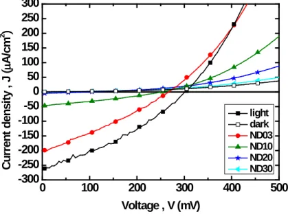
Fig.5.4 Photocurrent to voltage characteristics of junctions under varied illumination
intensities. p.58 Fig.5.5 (a) EIS phase and (b) Nyquist plot of junctions under varied illumination
intensities. p.59
Fig.5.6 Photocurrent to voltage characteristics of junctions with different Cu2O deposition
time of (a) 8 hours, (b) 6 hours, and (c) 4 hours under varied
illumination intensities. p.60 Fig.5.7 Fig.5.7 (a) EIS phase and (b) Nyquist plot of junctions with positive voltages from 0V
to +0.6V, and (c) Mott-Schottky plot extracted from the EIS results. p.61
Fig.5.8 (a) EIS phase and (b) Nyquist plot of junctions under 0.2V bias. p.62
Fig.5.9 Mott-Schottky plot of junctions extracted from (a) middle frequency region and (b)
1
Chapter 1
Introduction
The demand of energy grows up very rapidly in recent years. Nearly everything that can make our life convenient is energy consuming, for example, machines, vehicles and electrical equipments. Although there are so many ways to produce energy, it is always insufficient and polluted. For instance, one of the major methods is the direct burning of fossil fuel, which can make serious air pollution by discharging carbon oxide and carbon dioxide. Except fossil fuel, nuclear power may be a more efficient way to produce energy, but it is very difficult to handle the nuclear waste. In the present, low pollutant producing, source abundant and non-expensive are the basic requirements for the new era energy. To produce energy sufficiently but not destroying our environment is an urgent issue.
One of the possible technologies for energy is the solar cell, which is a device that converting energy of sunlight to electricity directly. For the abundance, inexhaustibility of solar energy, and the least pollution production in the operation of solar cells, the photovoltaic device is a promising candidate for energy production in the future.
The working principle of the conventional solar cell is based on the properties of a p-n junction structure. Incident photons interact with electrons in the semiconductor bulk and cause the excitation of electrons to the conduction band. The build-in potential in the depletion region of the p-n junction causes separation of electrons in the conduction band and holes in the valence band. When electrons and holes are separated and drifted out of depletion region, each one will transport to corresponding electrode by diffusion because of the concentration gradient induced in the bulk material. Briefly speaking, the operation of a solar cell includes three major stages, absorption separation and transportation.
2
Although it is possible to attain sufficiently high light conversion efficiency in conventional semiconductor p-n junction structures, the contrary high cost in material purification limits the payback time seriously. The other disadvantage of silicon solar cells is the use of toxic chemicals in manufacture. To obtain a photovoltaic component better in terrestrial use, new architecture with less material consuming is required. The remarkable energy conversion efficiency achieved in dye-sensitized solar cell (DSSC) has demonstrated the possibility to gain high photovoltaic performance in relatively low material cost with a different solar energy harvesting architecture. Table1.1 [1, 2] are lists of the energy payback time of different solar cells; it is obvious that the payback time for DSSC is much shorter than other solar cells; just as mentioned before.
Dye sensitized solar cell, proposed by M.Grätzel at 1991 [3], works different from conventional structures. The basic structure of the device is shown as Fig.1.1 [4], the specially designed dye molecule, as the major light absorber, are on one side chemically absorbed on the surface of titanium dioxide deposited on TCO (transparent conducting oxide) glass
substrate while the other side is immersed in I- / I3 -electrolyte with catalytic Pt or carbon layer
as the counter electrode. Upon light absorption from TCO side, the electron at the ground state of the dye is excited to the excited states. After that, the electron in the excited state
inject ultra fast to the conduction band of TiO2. The injected electrons will diffuse in the TiO2
layer due to the concentration gradient before reaching the anode of the cell. The left hole in
the ground state of dye will be reduced by I- / I3 -ionic electrolyte.
However, there are severe problems for present DSSCs such as solvent evaporation, dye degradation, and seal imperfection in the encapsulation of liquid electrolyte in these cells. Several solid state materials are proposed to replace the liquid redox electrolyte to solve these
problems that limited the efficiency of dye-sensitized solar cells. For example, RT molten
salts [5], conducting organic polymer [6], polymer gel electrolyte [7] and p-type semiconductors [8] are suitable as hole conductor in cells. There are some criteria for these
3
materials, such as transparency in visible spectrum, good conductivity to hole, and proper
method to deposit in the nano-porous TiO2 structure. The basic structure of solid-state DSSC
is shown in Fig.1.2 [9], it is similar to liquid DSSC except for the replace of liquid electrolyte to solid-state material.
Since the TiO2 thickness for DSSC should be over several micrometers, there are not many suitable processes to deposit the hole conductor on the nano-porous film to form the hetero-junction well. Solvent removal method and the electrochemical deposition method are
the two common ways to fill the pores of the TiO2.
Solvent removal method is a way that a p-type semiconductor is usually dissolved in a
suitable solvent and filled into nano-porous TiO2 film by dipcoating or spicoating. After that,
the sample was heated to evaporate the solvent. It is a relatively easy way to deposit materials such as CuSCN [10], CuI [11], and spiro-OMeTAD [12], and the performance of solid-state DSSC used these materials are already demonstrated. However, forming a good contact with
the dyed TiO2 particles by this method is very hard since dye may detach from the TiO2
surface in deposition process, and lead to the low efficiency of solid-state DSSCs.
Electrochemical deposition method is normally more material restricted and is dependent on both the characteristics of deposited material and the surface properties of the material on which it is deposited. Therefore, if we want to fill the porous structure well, the best
deposition condition must be found. For example, it has been showed the growth of CuInSe2
within porous TiO2 was controllable by using modified electrolyte compositions [13]. Besides,
CuSCN was already reported to be electrochemically deposited onto dye adsorbed ZnO by
this method and the efficiency was 1.5% [14], and it was also deposited onto TiO2
nano-crystalline surface with demonstrating p-n hetero-junction characteristics [15,16].
Cuprous oxide (Cu2O) is an appropriate p-type material in solar energy application
because it is direct band gap, abundant in element on the earth, and is non-toxic. Although
4
methods highly limited its use. Direct oxidation of copper metal cannot be applied to other
substrates. In spite of oxidation, another method was proposed to deposit Cu2O nano-particle
onto ZnO nanowire, and the photovoltaic characteristics are observed on the all oxide
composed hetero-junction [17].However, the reported ZnO thickness with this method was
still less than 3 um.
In this thesis, we have applied he electrochemical deposition method to directly deposit
Cu2O onto nano-porous TiO2 film. By applying appropriate constant current level, we were
able to control the growth rate of Cu2O within the nano-porous network and Cu2O was
successfully filled the TiO2, which its thickness is more than 5μm. Most important of all, the
whole fabrication flow is quite simple and is environmentally benign. The measured electrical characteristics of this all oxide composed hetero-junction had shown the similar behavior with the conventional p-n junctions. By applying different measurement techniques we explored the preliminary knowledge about this bulk hetero-junction composed by two wide band-gap oxides.
5 Table 1.1
Table 1.1 Energy payback time of different type solar cells. [1, 2]
6
7
Chapter 2
Experimental Methods
2.1 Materials and equipments used in fabrication
Used materials and chemicals Substrate
Glass/ITO 7 Ω/□
Glass/FTO 10 Ω/□
Glass/FTO 20 Ω/□
Glass/FTO 30 Ω/□
TiO2 nano-crystalline powder
TiO2 P25 Degussa
Ingredient of TiO2 paste
Alpha terpineol SHOWA
Ethyl cellulose SHOWA
Acetic acid SHOWA
Chemicals of electrochemical deposition
Cupric sulphate SHOWA
Lactic acid SHOWA
8
Equipments in device fabrication
Microprocessor pH Meter (SUNTEX SP-2200)
Atmospheric Anneal Furnace (KH Union Co., Ltd)
Backend Vacuum Annealing Furnace (Best Champion Technology Co., Ltd)
Sputtering System (Ion Tech Microvac 450CB)
E-gun Evaporator (ULVAC EBX-8C)
2.2 Equipments for characterization of materials
Surface Profiler (Dektak 3030)
Scanning Electron Microscope (Hitachi S-4000)
High-Resolution Scanning Electron Microscope
& Energy Dispersive Spectrometer (Hitachi S-4700I)
X-Ray Diffractometer (PANalytical X'Pert Pro (MRD))
9
2.3 Electrochemical deposition experiments
Electrochemical deposition is an attractive method for preparing a variety of materials. It offers the advantages of low cost and high purity. A wide range of oxide
semiconductors such as TiO2 [18], ZnO [19], and CdO [20] were also synthesized by
this method. Besides, there are many studies on electrochemical deposition of Cu2O
films [21-28]. The Cu2O film can be synthesized in a three-electrode system
containing CuSO4-based aqueous solution by two kinds of methods - galvanostatic
method and potentiostatic method.
For the application to solid-state DSSC, it is necessary to find the best condition
to fill the porous TiO2 well to for a good contact. Even for the static current condition,
it was not always possible to obtain a fully filled bulk hetero-junction; similar to the
electrochemical deposition of CuInSe2 onto TiO2 nano-particle or nano-tube proposed
before [28], it was observed that the applied condition apparently influenced the pore-filling ability. With different conditions, we can achieve the different deposition mechanism, which is related to the ambipolar diffusion of ions with the nano-porous films.
2.4 Photo-electrical measurements
2.4.1 Current-voltage (I-V) measurement
The basic I-V measurement included two parts - the light source and the electrical measuring system. The solar simulator consists of Newport Oriel 96000 150W Xe lamp and AM1.5G filter 81094; the optical power of incident light was measured by
10
the thermopile detector 818P-010-12 and calibrated to 100mW/cm2before measuring.
The electrochemical potentiostat / galvanostat EG&G model 273A was connected to the device in two probing modes to characterize the I-V properties.
2.4.2 Electrical impedance spectroscopy (EIS) [29- 31]
The setup of EIS measurement was basically the same as the I-V measurement system, except that EG&G model 1025 Frequency Response Detector was connected to the electrochemical potentiostat / galvanostat EG&G model 273A. In the EIS measurement, small voltage oscillation signals with constant amplitude and different
frequencies V0eiωt were applied, and the corresponding current responses
I(ω)ei(ωt+φ) were analyzed. Then the impedance Z(ω) = V0eiωt
I(ω)ei(ωt+φ)= Z0(ω)eiφ,
where φ is the phase difference, can be acquired. Electrical impedance spectroscopy
measures the variation of impedance at different frequencies, so it is a trace of the variation of the impedance of measured sample.
Normally, the measurement for DSSC was done under the standard illumination with DC bias applied. The value of the DC bias was selected to be the open-circuit voltage of the measured device so that the device was under the static condition, i.e. there was almost no DC current when the measurement was proceeding. If not specially claimed, the conditions for EIS measurement in the experiment were always that the AC amplitude was of 5mV descending from 500 kHz to 0.01 Hz and DC bias equaled to open-circuit voltage.
11
Chapter 3
Electrochemical Deposition
and Material Analysis
The reason of why we want to fabricate solid-state DSSC had been introduced in
chapter1. Electrochemical deposition method seems to be a good way to deposit Cu2O on the
surface of nano-porous TiO2 film to form a bulk hetero-junction. However, the best condition
of electrochemical deposition must be found before using Cu2O as a hole collector. In this
chapter, the details of deposition condition and related material analyses are examined. All
these results can help us to not only find the best condition for Cu2O deposition but also
understand the properties of Cu2O with different deposition condition. It can provide the
meaningful reference to the later works.
3.1 Deposition conditions
3.1.1 Cu
2O deposition mechanism
The possible reaction during Cu2O deposition can be described by the following
equations:
2Cu2+ + 2e-1 + 2OH- → Cu2O + H2O (1)
Cu2+ + 2e-1 → Cu (2)
Cu2O + 2e-1 + 2H+ → 2Cu + H2O (3)
It is obvious that equation (1) and equation (3) are pH dependent, at lower bath pH value the metallic Cu may form according to reaction(3). The films deposited at
12
pH 7 is a compisite of Cu2O and Cu; while the film deposite at bath pH value larger
than 9 is pure Cu2O. It means that with higher OH- concentration the Cu2O could be
deposited easily. Besides, with the the the bath pH increased from 9 to 13, the prefered
Cu2O orientation also changed from (200) to (111). And all the results mentioned
above corredponded to the previously proposed paper [32, 33]. According to these results discussed before, it is obvious that the pH value of solution is an important
factor in the synthesis of Cu2O.
3.1.2 Cu
2O Deposition methods
To electrochemically deposit Cu2O onto the TiO2 nano-particle, the solution was
referenced to previously proposed one [21]: 0.4M cupric sulphate, 3M lactic acid, and sodium hydroxide was added to modify the pH value. The deposition was carried out at the set temperature in the standard three electrode configuration, as shown in Fig.3.1, Ag/AgCl be the reference electrode whereas Pt be the counter electrode, and the applied bias were controlled by the potentiostat.
Two types of electrochemical deposition methods, galvanostatic method and potentiostatic method, were both examined in our experiment. Fig.3.2. (a) shows the monitored deposition voltage profiles at constant current level. The voltage drastically change at the early initial stage and afterward became neatly steady for each
deposition processes. It is easy to control the deposited Cu2O thickness by the static
deposition rate estimated from galvanostatic method. Compared with it, the potentiostatic method with constant voltage level shows the time dependent deposition current profiles, as shown in Fig.3.2 (b); and it is hard for us to control the deposition process.
13
3.1.3 Cu
2O deposition conditions
Even with the current static approach, a fully filled BHJ was not always accomplished; similar to the previously proposed electrochemical deposition of
CuInSe2 onto TiO2 nano-particle or nano-tube [13], the applied pH value of solution
(solution composition) did influence the pore-filling ability of the deposited material. Fig.3.3 (a) shows the voltage profiles in bath solution with pH10, it is shown that the spontaneous potential oscillation is observed. It is a normal phenomenon in the alkaline Cu(II)/taetrate and lactate system when applying current level to electrochemical deposition [36, 37], and was caused by the variations in pH close to the electrode surface during the oscillation process. When spontaneous potential
oscillation is observed, both Cu and Cu2O are deposited. The oscillation period is
effected by pH value and temperature. Besides, the current density also decides when the oscillation happened. A high current density favors Cu deposition and a low
current density favors Cu2O deposition. As shown in fig.3.3 (a), we can get static
deposition voltage when the applying current density is lower enough. Fig.3.3 (b) shows the voltage profiles with different pH value but the same current level
(28μA/0.09cm2). As the pH increased, the voltage shifted to more negative value,
which was due to the pH dependent deposition mechanism.
Although we can get static deposition rate with lower enough current density in
solution with pH10, the deposition rate is too low to fill the nano-porous TiO2 film.
Beside, instead of plainly cumulative deposition from the bottom to the top, the Cu2O
also appeared on the top portion of nano-porous TiO2; therefore, the formation of a
complete bulk hetero-junction cannot be achieved, as shown in Fig.3.4. As a result, we use the solution with higher pH value, which we can apply the higher current density
14 and hence get higher deposition rate.
Fig.3.5 shows the voltage profiles at different current levels at solution with pH10. We found that the magnitude of voltage was closely related to the applied
current level; larger current level, higher voltage and Cu2O deposition rate were
observed if all the other deposition conditions were kept the same. In addition, different substrates did not lead to different results. This is due to the presence of an
intentionally deposited condensed TiO2 layer on top of the substrates, which could
prevent the formation of reversed leakage path and shunt resistance lowering arising
from the direct contact of Cu2O with the substrates. As a result, negligible difference
in the deposition can be anticipated if the distinct substrates had similar sheet
resistance. This result also helped us justify whether or not the Cu2O/TCO junction
was formed. If there was unwanted great shunt leakage paths in the complete structure, it will become an ohmic junction instead of a rectified junction. Fig.3.6 shows the
cross sectional SEM images of the film deposited with pH 14. The growth of Cu2O
starting from the bottom of TiO2 was obviously observed, and the growth rate was
found to be nearly constant and around 20nm/min.
3.2 Material Analyses
Once a well filled junction was obtained, the material analyses are needed to be conducted in order to characterize the physical properties of the deposited film. Fig.3.7
shows the XPS and XRD results of the sample prepared with 300μA/cm2 for 2 hours
with 1.5μm porous TiO2 and 20nm sputtered TiO2 barrier layer on the ITO substrate.
Three different pH values, 12.9, 14, and 14.7, are adapted as the solution pH value.
15
952.0eV and 932eV respectively, which agree well with the reported values for the cuprous oxide [38,39], and the CuO-related shake satellites were weak for samples with pH12.9 and pH14. We noted that when pH value reaches to 14.7, the obvious
CuO-related shake satellites appear. Under this condition, we cannot get pure Cu2O
film. From the XRD diffraction spectra in Fig.3.7 (b), we obviously observed the
major Cu2O crystalline peaks without Cu or CuO peaks appearing. Besides, the
sample with pH14 shows the strongest dominant Cu2O (111) orientation. The TiO2
anatase peak of the host layer below Cu2O also could be found in the spectra, the rutile
phase of P25, however, was relatively weak so that this phase was not be easily identified in the figure.
Fig.3.8 shows the XPS and XRD results at pH14 for 2 hours with different
current level ranges from 40μA/cm2 to 400μA/cm2. For samples with current density of
40μA/cm2, 80μA/cm2 and 200μA/cm2, the CuO-related shake satellites were very
obvious in Fig.3.8 (a). And their XRD results in Fig.3.8 (b) showed weak Cu2O
orientation, which corresponded to the XPS results. Samples with current densities of
300μA/cm2 and 400μA/cm2 showed the Cu2O characteristics in the XPS results.
Therefore, their dominant Cu2O (111) orientation is obviously strong. Even through,
the (111) orientation of sample with 300μA/cm2 was larger than the 400μA/cm2 one.
As a result, from the XPS and XRD result discussed before, the deposition
conditions with pH12.9 or pH14 and current density of 300μA/cm2 may be the best
condition to deposit pure Cu2O on the nano-porous TiO2 films.
According to the previously proposed paper [40], vacuum annealing of CuO bulk
can make the surface of CuO bulk transform to Cu2O by decreasing the contaminant
of oxygen. And the experiment result was verified by the XPS spectrum. In the thesis,
vacuum annealing is also applied in an attempt to get purer Cu2O composition. Fig.3.9
16
vacuum annealing conditions. All samples are heating in about 5e-7 torr for 15 minutes with different temperatures. It makes no difference in the condition of 100℃ to 300℃ at vacuum except for 300℃ in 0.3torr N2, in which the CuO component become a little larger.
In order to calculate the deposition rate, we deposit the Cu2O film with different
time and use the SEM technique to investigate its cross-sections and top-views.
Fig.3.10 shows the SEM images, it was shown that Cu2O growth from bottom layer of
nano-porous TiO2 to its upper layer, and the thickness of Cu2O were about 300nm,
600nm, and 3000nm for deposition time of 15 minutes, 30 minutes, and 150 minutes,
respectively. And the deposition rate was about 20nm/minutes. Besides, with longer
deposition time, the number of Cu2O grains on the surface of nano-porous also
17
18 (a) 0 100 200 300 400 500 600 -800 -700 -600 -500 -400 Vo lt a g e , V ( m V) Time , t (sec) (b)
Fig.3.2 Deposition curve of two kinds of methods: (a) galvanostatic method, and (b) potentiostatic method. 0 100 200 300 400 500 600 18 20 22 24 26 28 30 32 34 36 38 C u rr en t d en si ty , J ( µA/ c m 2 ) Time , t (sec)
19
(a)
(b)
Fig.3.3 (a) Voltage profiles with different deposition current density in bath solution with pH 10.
(b) Voltage profiles with different current pH value at the current density of
10μA/0.25cm2. 0 100 200 300 400 500 600 -1100 -1000 -900 -800 -700 -600 -500 -400 -300 -200 -100 0 Vo lt a g e , V ( m V) Time , t (sec) pH 10 50µA/0.25cm2 25µA/0.25cm2 10µA/0.25cm2 0.0 5.0x10² 1.0x10³ 1.5x10³ 2.0x10³ 2.5x10³ -850 -800 -750 -700 -650 -600 -550 -500 Vo lt a g e , V ( m V) Time , t (sec) pH14.7 pH14 pH12.9
20
Fig.3.4 SEM images of as depositing nano-porous samples at 10μA/0.25 cm2 for 6 hours
(pH 10), and the identified Cu2O regions were indicated in the figures.
Fig.3.5 The voltage-time variations at different current levels with samples of P25
TiO2, 20nm TiO2 thin film, and the selected substrates, (1) 200μA/cm2 ITO,
(2) 300μA/cm2 FTO, (3) 300μA/cm2 ITO, and (4) 500μA/cm2ITO.
0 1 2 3 4 5 -700 -650 -600 -550 Vo lt a g e , V ( m V) Time , t
(
103sec)
200µA/cm2 ( ITO ) 300µA/cm2 ( FTO ) 300µA/cm2 ( ITO ) 500µA/cm2 ( ITO )21
Fig3.6 SEM images of as depositing nano-porous samples at current density 300μA/cm2 for
22 (a) (b)
Fig.3.7 The (a) XPS, and (b) XRD results at deposition current density of 300μA/cm2 for
2 hours with different pH values of (1) pH12.8, (2) pH14, and (3) pH14.7.
930 940 950 960 970 pH12.9 pH14 pH14.7 Int e ns it y
Binding energy (eV)
20 30 40 50 60 70 80 pH12.9 pH14 pH14.7 TiO2 (101) Anatase ITO ITO ITO Cu 2O (311) Cu2O (220) Cu2O (200) Cu2O (111) Int e ns it y Angle 2θ o
23
(a)
(b)
Fig.3.8 The (a) XPS and (b) XRD results at bath solution with pH14 for 2 hours at different
current levels of (1) 40μA/cm2, (2) 80μA/cm2, (3) 200μA/cm2, (4) 300μA/cm2,
and (5) 400μA/cm2. 925 930 935 940 945 950 955 960 965 970 40 µA/cm2 80 µA/cm2 200 µA/cm2 300 µA/cm2 400 µA/cm2 Int e ns it y
Binding energy (eV)
20 30 40 50 60 70 80 Cu2O (311) Cu2O (220) Cu2O (200) Cu2O (111) TiO2 (101) Anatase ITO ITO ITO Int e ns it y Angle 2θ o
24
(a)
(b)
Fig.3.9 The (a) XPS and (b) XRD results at current density of 300μA/cm2 and bath solution
with pH14 for 2 hours at different vacuum annealing conditions of (1) w/o annealing, (2) 100℃ 15minutes, (3) 200℃ 15minutes, (4) 200℃ 15minutes in N2 0.3 torr, and (5) 300℃ 15 minutes. 925 930 935 940 945 950 955 960 965 Int e ns it y
Binding energy (eV)
w/o vac. anneal 100oC 15min. 200oC 15min. 200oC 15min. in N2 0.3torr 300oC 15min. 20 30 40 50 60 70 80 TiO2 (101) Anatase ITO ITO ITO Cu2O (311) Cu2O (220) Cu2O (200) Cu2O (111) Int e ns it y Angle 2θ o
25 (a) (b) (c) (d) (e) (f)
Fig.3.10 SEM cross-sections and top views with different deposition time of (a)(b) 15 minutes, (c)(d) 30 minutes, (e)(f) 150 minutes.
26
Chapter 4
Junction Characterizations
Based on previous results, we find the better conditions for Cu2O deposition and have the
basic understanding of material characteristics. In this chapter, we successfully fabricate the
Cu2O bulk hetero-junction and investigate its characteristics by electrical measurements. With
the study of the obtained results, we can comprehend the basic characteristics of the junction and compare it with the properties of conventional p-n junction. Furthermore, we acquire the frequency response by applying electrochemical impedance spectroscopy (EIS) under different conditions to get the information about charge diffusion and recombination mechanism inside the structure.
4.1 Fabrication process
27
The fabrication flow is depicted as Fig.4.1. In the beginning, the TCO (20Ω/
FTO or 10Ω/ ITO) glasses were ultrasonically cleaned in ethanol first and then in
de-ionized water. 20nm amorphous thin film TiO2 was reactively sputtered onto the
TCO substrate before the coating of TiO2 nano-particles. The preparation of TiO2
paste was referenced to the previous method [41]; the paste was coated on TCO glass
substrate by the doctor blade method. After that, the TiO2 film was sintered in
atmospheric ambient at 450℃ for 2 hours with air flow. The thickness of the prepared
TiO2 was determined by Surface Profiler
For electrochemical deposition, the samples were immersed in the CuSO4-based
aqueous solution at room temperature; the solution consisted of 0.4M cupric sulfate and 3M lactic acid and the pH of the bath was adjusted by the addition of sodium hydroxide. The deposition was carried out at the set temperatures in the standard three electrode configuration, Ag/AgCl be the reference whereas Pt be the counter, and the applied bias were controlled by the potentiostat. After the 4 to 6 hours deposition, the reddish sample was moved out from the solution and rinsed by ethanol and water and was baked to remove residual solution on the surface.
For electrical measurement, 150nm Au contact pad was E-gun evaporated onto
the Cu2O surface; the complete Au/Cu2O/TiO2/TCO junction structure is shown in
Fig.4.2. Then junction properties were measured by the pontentiostat in two electrode configuration.
28
4.2 Photo-electrical analyses
4.2.1 Basic characteristics of junction
The current density of device with different deposition conditions under both forward and reverse bias is presented in Fig.4.3. The deposition current level we
applied was of 50μA with active area 0.16cm2 for 4 hours on the 1.5μm P25 porous
layer with 20nm TiO2 barrier layer under it. Rectifying characteristic of the junctions
was clearly observed, and both forward and reverse currents increased with the raise of measured temperature. It is similar to the conventional p-n junction.
Fig.4.4 (a) displays the I-V characteristics of junctions with different deposition conditions. All the three devices showed slope transition in the forward region as the conventional p-n junction did. The forward current densities differed most in the low voltage region. Besides, larger reverse current densities were obtained for junctions with larger current densities in low voltage region. So, the current in the low voltages region was postulated to be provided by the recombination centers, and these trap centers also acted as the dominant generation source of the reversed current. Even though the exact mechanism and the locations of these traps could not be clearly clarified by available data now, the amount of these centers should be related to the
composition of Cu2O for the different I-V characteristics with the different deposition
conditions.
Fig.4.4 (b) is the optical responses of these junctions, and the highest photo-voltage and photocurrent achieved under 1 sun illumination were 0.38V and
0.21mA/cm2 for the device with the lowest recombination current. This result was
29
interface traps. Since the junction will be influenced by these traps, it is important to lower down the number of these recombination centers before applying to the DSSCs. Fig.4.5 shows the impedance spectrums under zero bias of these junctions. There
were no apparent difference of the impedance magnitude at higher frequency region, but the impedance magnitude deviated apparently at low frequency region. As a result, the dominant electron transfer mechanism around zero bias was via the interface or bulk trapping states. Noted that the characteristic frequencies for these samples were separated obviously, and the characteristic frequencies for these three samples were consistent with those exhibited in recombination current and impedance magnitude as well. Hence, the characteristic frequencies could be related to the recombination rate as in the conventional DSSC results [42]. It was reasonable that the device with lower characteristic frequency, which is related to the smaller recombination rate, shows better optical performance.
Based on the above experimental results and discussion, it was known the
Cu2O/TiO2 bulk hetero-junction had certain similarities with a conventional p-n
junction. With both DC I-V and AC EIS analyses, we could evaluate the recombination behavior of this 3D disordered junction. It was thought that the recombination behavior is the most important factor that limited the junction performance. Therefore, to comprehend the cause of the defects and then suppress the formation of these traps is the purpose we pursuing now.
30
4.2.2 Effect of other factors
In this section, we investigate the IV and EIS results with many groups of conditions. This help us to not only further understand the effect of different conditions but also find the best condition to achieve better device performance. If not
specially claimed, the conditions for Cu2O deposition are galvanostatic deposition
method with current density 28μA/0.09cm2 for 6 hours in the CuSO4-based aqueous
solution with pH14.
First of all, Cu2O was deposited on the TiO2 layer with two sintering conditions,
375℃ for 2 hours and 450℃ for 3 hours. The deposition conditions were maintained the same for the two junctions and the substrates used were ITO for 375℃ 2 hours and FTO for 450℃ 3 hours. And the sheet resistances of the two substrates are the
same (20Ω/) after sintering. The dark current and photocurrent to voltage
characteristics are shown in Fig.4.6 (a) and (b), respectively. It was obvious that the
junction with TiO2 sinter condition of 450 ℃ for 3 hours showed smaller
recombination current and reverse current than the one with 375℃ for 2 hours; and the optical result also showed the larger photocurrent but nearly the same
photo-voltage for junction with TiO2 sinter condition of 450℃ for 3 hours. From the
results, it seems that junction fabricated by TiO2 film with sinter condition of 450℃
for 3 hours, which showed smaller recombination current and larger photocurrent, is a better condition. Fig.4.7 (a) and (b) displays the dark current and photocurrent characteristics of junctions with different substrates. Noted that the sinter conditions are 375℃ 2 hours and 450℃ 3 hours for the ITO and FTO substrates, respectively.
Again, those junctions on FTO substrates, which TiO2 sinter condition was 450℃ 3
31
FTO substrates with 10Ω/ was larger since its sheet resistance is smaller than the
30Ω/ one.
In Fig.4.8 (a) and (b), the EIS phase plot and Nyquist plot are presented. Although the Nyquist plot showed the same trace except for the impedance value, the peak frequencies which is related to recombination mechanism shifted to higher value
for junctions with TiO2 sinter condition of 450℃ 3 hours. It seems contradictory to
the I-V characteristics shown before since the one with small recombination current
showed larger peak frequency. But the TiO2 sinter conditions are different for
junctions fabricated on different substrates, so it is obvious that the divergence in peak
frequency values is related to the TiO2 surface properties. From the experiment results,
although junctions with TiO2 sinter condition of 450℃ 3 hours show higher peak
frequency values, it is not related to the higher recombination currents. Besides, the high frequency circle in Nyquist is obvious, and we assume the circle is related to the
Cu2O/TiO2 junction since the frequency range is reasonable.
Next, another experiment was performed to clarify whether the deposition time affect the electrical characteristics of junction. Basic I-V characteristics of these junctions are depicted in Fig.4.9 (a) and (b). The dark I-V curves were quite similar except for a little deviation in low voltage region, and the difference of recombination current is also due to this deviation. The optical characteristics displays that the
junction with Cu2O deposition time of 4 hours showed larger photo-voltage, which is
related to its smaller recombination current in the dark I-V curves. Fig.4.10 (a) and (b)
shows the EIS results of junctions with different Cu2O deposition time, and it was
found that these three junctions showed the similar impedance trace in Nyquist plot. It
was noted that for junctions with longer Cu2O deposition time, the peak frequencies
shifted to lower values, which meant the improved recombination mechanism. It is
32
deposition process, and the junctions after repaired may showed better recombination characteristics. As a result, for samples with longer deposition time, the junctions will
be repaired more and the numbers of recombination centers between the Cu2O/TiO2
junctions will be eliminated.
Third, for the further application to the DSSC, we examined the effect of the
deposition mechanism after the TiO2 layer was coated with dye. It is reasonable that
the surface property with dye absorption is very different from surface without dye absorption, and the deposition condition will not be the same for different surface properties. Basic I-V characteristics of the devices with dye absorption are depicted in Fig.4.11 (a) and (b). It was shown that both the devices with dye absorption showed larger recombination currents and reverse currents. The optical characteristics also displayed the same results, which the devices with dye absorption showed the worse performance than those without dye absorption, especially the one with N3 dye. Besides, the deviation between the two dyed devices came from the different binding
characteristics of dye with the TiO2 surface. All the divergence of the I-V
characteristics for these devices may be ascribed to the properties of TiO2 surfaces,
which is very different from each other. Hence, when we apply the same deposition condition on surfaces with different properties, the mechanism for deposition must be
different. Furthermore, the detachment of dye which absorbed on the TiO2 surface also
affected the deposition mechanism. In order to confirm this postulation, EIS measurement is conducted and the results are presented in Fig.4.12. Fig.4.12 (a) shows the result of EIS phase, and it was found that the peak frequency, which corresponded to recombination mechanism, of devices with dye absorption shifted to higher value in phase plot. Fig.4.12 (b) displays the Nyquist plot, and it is apparent that the impedances of circles related to recombination mechanism also decreased with the increased values of peak frequencies in phase plot.
33
In the final part of the section, we applied the same deposition conditions in the solutions with different pH values in order to investigate the effect of deposition pH value. Fig.4.13 (a) and (b) displays the dark current and photocurrent to voltage characteristics of junctions with pH value of 14.7, 14, and 12.9. The junction with pH 14 showed the best I-V characteristic and the junction with pH 14.7 showed the worse characteristic which may be due to the change of composition as discussed before. It was also found that the junction with pH14.7 showed the worse characteristic and the other junctions showed the similar characteristics in the photocurrent to voltage results. The EIS characteristics of these junctions are also depicted in Fig.4.14 (a) and (b), it is obvious that junction with pH 14 showed the lowest peak frequency than others in the phase plot. Again, the junctions with pH14 and pH12.9 showed the similar trace in the Nyquist plot except for the magnitudes of impedance, and the result of junctions with pH14.7 is very different. From the results we investigated before, pH14 may be a
better condition within the three pH values we used to deposit the Cu2O films.
4.2.3 Effect of vacuum annealing
To achieve the best electrical characteristic, except for the request of deposition methods, the composition of p-type materials we deposited is also an important issue.
As a result, high purity of p-type Cu2O film is our purpose. In previously proposed
paper [43], high vacuum treatment was adapted and the surface composition of CuO
and Cu2O was investigated by XPS and XAES. In our research, high vacuum anneal
treatment was also applied in order to get the purer Cu2O composition. The
characteristics of junctions with different vacuum annealing treatments were discussed in this part.
34
Experiment was performed to investigate the effect of vacuum annealing temperature. Noted that the annealing pressure was about 5e-7 torr and the annealing time was 30 minutes. Fig.4.15 (a) are the dark current to voltage characteristics of junctions with different vacuum annealing temperatures, it was found that junctions with vacuum annealing treatment shows larger recombination currents than junctions without treatment except for the one with 300℃ annealing. Besides, the junction with 100 ℃ annealing showed similar diffusion current levels with the one without annealing, and both were larger than these two junctions with 200℃ annealing. Besides, for junctions with 200℃ vacuum annealing treatment, the one in N2 ambient (about 0.3 torr) showed worse performance than the other. Fig.4.15 (b) shows the photocurrent to voltage characteristics of these junctions with different vacuum annealing conditions, and it displayed the same trends that junctions with smaller recombination currents showed better optical performance. It is mentioned that the junctions with 300℃ annealing showed very small current levels both in forward and reverse bias regions, but the rectify characteristic was not investigated.
With the results we investigated, it seemed that vacuum annealing treatment cannot provide better performance. From the analysis of XPS results about different vacuum annealing conditions before, it was shown that the composition of deposited
Cu2O with 100℃, 200℃, and 300℃ vacuum annealing were nearly the same. So the
deviation of these junctions cannot be ascribed to the change of Cu2O composition. As
a result, it is reasonable to postulate that the vacuum annealing treatment may break the junction and hence degrade the electrical characteristics.
In order to improve our postulation, EIS measurement was conducted, and the result is shown in Fig.4.16. Figt.4.16 (a) is the phase plot, it was found that junctions with higher vacuum annealing temperature showed lower peak frequencies values except for the 100℃ one, which showed a little larger value of peak frequency. The
35
contradictory results of phase plot compared to the I-V characteristics can be
explained by the destruction of Cu2O/TiO2 junctions. The recombination time, which
is proportional to the reverse frequency, became smaller because the Cu2O/TiO2
junction was broken with the elevated temperatures. The Nyquist plot is also shown in Fig.4.16 (b) and (c), it is obvious that the circles related to the high frequency region became larger with the increase of annealing temperature. It may be reasonable to
postulate the circles with high frequency region is related to the Cu2O/TiO2 junction
since the composition and crystal phase of TiO2 itself do not change in the annealing
36
Fig.4.2 The complete Au/Cu2O/TiO2/TCO junction structure for measurement and the
SEM cross-sectional image with indicated corresponding layers.
Fig.4.3 Forward and reverse current-voltage characteristics of the typically fabricated junction:
Cu2O 300μA/cm2 4hr, P25 TiO2 1.5μm, 20nm sputtered TiO2 at elevated temperatures.
Inserted picture is the enlarged reverse part.
-400 -200 0 200 400 600 800 -100 0 100 200 300 400 500 600 -800 -600 -400 -200 0 -140 -120 -100 -80 -60 -40 -20 0 20 C u rr en t d en si ty , J ( µA/ c m 2 ) Voltage , V (mV) 298K 308K 318K
37
(a)
(b)
Fig.4.4 (a) Forward and reverse current-voltage characteristics in log scale of junctions and (b) 1sun illuminated current-voltage characteristics of junctions with three different
Cu2O depositing conditions:(1) 28μA/0.09cm2 4hrs, (2) 28μA/0.09cm2 hrs, and (3)
18μA/0.09cm2 8hrs. All bottom layers were P25 TiO2 1.5μm, 20nm sputtered TiO2.
-800 -600 -400 -200 0 200 400 600 800 0.1 1 10 100 1000 10000 C ur re nt de ns it y , l og IJ I (µ A/ c m 2 ) Voltage , V (mV) 28µA/0.09cm2 4hrs 28µA/0.09cm2 6hrs 18µA/0.09cm2 8hrs 0 100 200 300 400 500 -250 -200 -150 -100 -50 0 50 100 150 200 250 300 350 28µA/0.09cm2 4hrs 28µA/0.09cm2 6hrs 18µA/0.09cm2 8hrs C ur re nt de ns it y , J ( µA/ c m 2 ) Voltage , V (mV)
38
Fig.4.5 Impedance results of junctions with three different Cu2O depositing conditions:
(1) 28μA/0.09cm2 4hrs, (2) 28μA/0.09cm2 6hrs, and (3) 18μA/0.09cm2 8hrs
All bottom layers were P25 TiO2 1.5 , 20nm sputtered TiO2. All the samples
were measured at zero bias, and the recorded frequency was ranged from 100kHz to 1mHz. m µ 10-2 10-1 100 101 102 103 104 105 0.0 200.0k 400.0k 600.0k 800.0k 1.0M 1.2M 0.0 0.5 1.0 1.5 2.0 I Im p e d a n c e I , IZ I (Ω ) Frequency , f (Hz) 28µA/0.09cm2 4hrs 28µA/0.09cm2 6hrs 18µA/0.09cm2 8hrs p h ase ( R ad )
39 (a)
(b)
Fig.4.6 (a) Dark current and (b) photocurrent to voltage characteristics of junction with
different annealing temperatures of TiO2 : (1) 375℃ 3 hours (b) 450℃ 2 hours.
-800 -600 -400 -200 0 200 400 600 800 0.1 1 10 100 1000 C ur re nt de ns it y , lo g IJ I (µ A/ c m 2 ) Voltage , V (mV) 375oC 3hr 450oC 2hr 0 100 200 300 400 500 -300 -250 -200 -150 -100 -50 0 50 100 150 200 250 300 375oC 3hr 450oC 2hr C u rr en t d en si ty , J ( µA/ c m 2 ) Voltage , V (mV)
40 (a)
(b)
Fig.4.7 (a) Dark current and (b) photocurrent to voltage characteristics of junctions fabricated on different substrates:
(1) ITO: 20 Ω/, (2) FTO1: 10 Ω/, and (3) FTO2: 30 Ω/
-800 -600 -400 -200 0 200 400 600 800 0.1 1 10 100 1000 ITO FTO1 FTO2 C ur re nt de ns it y , l ogI J I (µ A/ c m 2 ) Voltage , V (mV) 0 100 200 300 400 500 600 -450 -400 -350 -300 -250 -200 -150 -100-50 0 50 100 150 200 250 300 350 400 450 ITO FTO1 FTO2 C ur re nt de ns it y , J ( µA/ c m 2 ) Voltage , V (mV)
41 (a)
(b)
Fig.4.8 (a) EIS phase and (b) Nyquist plot of junctions fabricated on different substrates:
(1) ITO: 20/ (2) FTO1: 10 Ω/ (3) FTO2: 30 Ω/.
10-2 10-1 100 101 102 103 104 0.0 0.5 P h ase ( R ad ) Frequency , f (Hz) ITO FTO1 FTO2 -100k 0 100k 200k 300k 400k 500k 0.0 20.0k 40.0k 60.0k 80.0k 100.0k Im (Z ) (Ω ) Re(Z) (Ω) ITO FTO1 FTO2
42 (a)
(b)
Fig.4.9 (a) Dark current and (b) photocurrent to voltage characteristics of junctions with
different Cu2O deposition time of (1) 3 hours, (2) 4 hours, and (3) 6 hours.
0 100 200 300 400 500 -200 -150 -100 -50 0 50 100 150 200 8 hrs 6 hrs 4 hrs C u rr en t d en si ty , J (µ A/ c m 2 ) Voltage , V (mV) -800 -600 -400 -200 0 200 400 600 800 0.01 0.1 1 10 100 1000 8 hrs 6 hrs 4 hrs C ur re nt de ns it y , l ogI J I (u A/ c m 2 ) Voltage , V (mV)
43 (a)
(b)
Fig.4.10 (a) EIS phase and (b) Nyquist plot of junctions with different Cu2O deposition time
of (1) 4 hours, (2) 6 hours, and (3) 8 hours.
10-2 10-1 100 101 102 103 104 105 0.0 0.2 0.4 0.6 0.8 1.0 1.2 Frequency , f (Hz) P h ase ( R ad ) 8 hrs 6 hrs 4 hrs 0.0 400.0k 800.0k 1.2M 0 100k 200k 300k 400k 500k 600k 8 hrs 6 hrs 4 hrs Im (Z ) (Ω ) Re(Z) (Ω)
![Table 1.1 Energy payback time of different type solar cells. [1, 2]](https://thumb-ap.123doks.com/thumbv2/9libinfo/8425586.180814/18.893.131.779.198.369/table-energy-payback-time-different-type-solar-cells.webp)
![HPSH [ 氧化數平衡反應式係數 ]](data:image/gif;base64,R0lGODlhAQABAIAAAP///wAAACH5BAEAAAAALAAAAAABAAEAAAICRAEAOw==)